Note: Descriptions are shown in the official language in which they were submitted.
CA 02631032 2008-05-23
WO 2007/067684 PCT/US2006/046666
METHOD OF PRODUCING AND OPERATING A LOW POWER
JUNCTION FIELD EFFECT TRANSISTOR
BACKGROUND
Field
Integrated circuits and devices, and methods of producing and/or using such,
are disclosed, such as MOS transistors and Junction Field Effect Transistors
(JFETs)
and circuits.
Background Information
Very Large Scale Integrated Circuits are being scaled to smaller dimensions
to gain greater packing density and faster speed in a continuation of the
trend of the
past thirty years. Currently, CMOS technology is being manufactured with sub-
100
nanometer (nm) minimum dimensions in 2005. Scaling CMOS with the minimum
line width below 100 nm presents numerous problems to designers of integrated
circuits. A few of the problems of the scaled CMOS transistors below 100 nm
are
highlighted below;
1. Power dissipation in CMOS is a big problem due to the high switching load
caused by the increase in gate capacitance per unit area as the thickness of
the gate dielectric is scaled.
2. The thickness of the gate dielectric used in the MOS transistor has been
scaled down to less than 20 angstroms. Thinning of the gate dielectric has
resulted in a significant amount of current through the gate dielectric as
voltage is applied to the gate electrode. This current is termed the gate
leakage.
3. The transistors conduct a finite current between the drain and source even
when the gate voltage is reduced to zero. This current is termed the source
drain leakage.
-1-
CA 02631032 2008-05-23
WO 2007/067684 PCT/US2006/046666
4. The result of the effects described above is CMOS circuits which conduct a
significant amount of current even when there is no activity (static current);
this undermines a key advantage of CMOS. Because of the static current, the
static power, or the power dissipated by the CMOS chip when there is no
activity, has become quite large, and at temperatures close to 100 degrees
centigrade, the static power dissipation can become nearly equal to the
dynamic power dissipation in CMOS circuits. As the CMOS technology is
scaled to 65 nm, the problem of leakage is becoming more severe. This
trend continues as the technology is scaled further to line widths of 45 nm
and below.
5. The lateral scaling of CMOS design rules has not been accompanied by
vertical scaling of feature sizes, resulting in three dimensional structures
with
extreme aspect ratios. For instance, the height of the polysilicon gate has
decreased only 50% while the lateral dimension of the.polysilicon gate has
been reduced by over 90%. Dimensions of the "spacer" (a component of a
CMOS transistor which separates the gate from the heavily doped source and
drain regions) are dependent upon the height of the polysilicon, so it does
not
scale in proportion to the lateral dimensions. Process steps which are
becoming difficult with scaling of vertical dimensions include formation of
shallow source and drain regions, their silicidation without causing junction
leakage, and etching and filling of contact holes to the source and drain
regions.
6. It is well known to those skilled in the art to measure power supply
leakage
current as an effective screen for detecting defects introduced in the
fabrication of the device. This method is sometimes referred to as the Iddq
test by those skilled in the art. This method is effective for CMOS with the
minimum line width above 350 nm. Scaling CMOS with the minimum line
width below 350 nm increases the inherent leakage current to levels
comparable to defect induced leakage current, rendering the Iddq test
ineffective. Biasing the well voltage of the MOS device to eliminate the
inherent leakage current introduces new elements of leakage such as gate
leakage, junction tunneling leakage, etc.
-2-
CA 02631032 2008-05-23
WO 2007/067684 PCT/US2006/046666
The prior art injunction field effect transistors dates back to the 1950s when
they were first reported. Since then, they have been covered in numerous texts
such
as "Physics of Semiconductor Devices" by Simon Sze and "Physics and Technology
of Semiconductor Devices" by Andy Grove. Junction field effect devices were
reported in both elemental and compound semiconductors. Numerous circuits with
junction field effect transistors have been reported, as follows;
such as:
Nanver and Goudena, "Design considerations for Integrated High-Frequency
p-Channel JFET's ", IEEE Transactions Electron Devices, vol. 35, No. 11, 1988,
pp. 1924 - 1933.
0. Ozawa, " Electrical Properties of a Triode Like Silicon Vertical Channel
JFET", IEEE Transcations Electron Devices vol. ED-27, No. 11, 1980, pp. 2115-
2123.
H.Takanagi and G.Kano, "Complementary JFET Negative-Resistance
Devices", IEEE Journal of Solid State Circuits, vol. SC-10, No. 6, December
1975,
pp. 509-515.
A.Hamade and J.Albarran, "A JFET/Bipolar Eight-Channel Analog
Multiplexer". IEEE Journal of Solid State Circuits, vol.SC-16, No. 6, December
1978.
K.Lehovec and R.Zuleeg, "Analysis of GaAs FET's for Integrated Logic",
IEEE Transaction on Electron Devices, vol. ED-27, No. 6, June 1980.
In addition, a report published by R. Zuleeg titled "Complementary GaAs
Logic" dated 4 August, 1985 is cited as prior art. The authors have also
published
the material in Electron Device Letters in 1984 in a paper titled "Double
Implanted
GaAs Complementary JFET's".
A representative structure of a conventional n-channel JFET is shown in
Figure 8. The JFET is formed in an n-type substrate 810. It is contained in a
p-well
region marked 815. The body of the JFET is shown as 820, which is an n-type
diffused region containing source (832), channel (838), and drain (834)
regions. The
gate region (836) is p-type, formed by diffusion into the substrate. Contacts
to the
source, drain, and gate regions are marked as 841, 842, and 840, respectively.
The
critical dimension of the JFET is the gate length, marked as 855. It is
determined by
-3-
CA 02631032 2008-05-23
WO 2007/067684 PCT/US2006/046666
the minimum contact hole dimension 850, plus the necessary overlap required to
ensure that the gate region encloses the gate contact. The gate length 855 is
significantly larger than 850. This feature of construction of the prior art
JFET
limits the performance of these devices, since channel length is substantially
larger
than the minimum feature size. In addition, the capacitances of the vertical
sidewalls of the gate diffusion to drain and source regions 861 and 862
respectively
are also quite large. The gate - drain sidewall capacitance forms the Miller
capacitance, a term known to those skilled in the art, and significantly
limits the
performance of the device at high frequencies.
SUMMARY
A method for using an inverter with a pair of complementary junction field
effect transistors (CJFET) with a small linewidth is provided. The method
includes
having an input capacitance for said CJFET inverter to be less than the
corresponding input capacitance of a CMOS inverter of similar linewidth. The
CJFET operates at a power supply with a lesser value than the voltage drop
across a
forward-biased diode having a reduced switching power as compared to said CMOS
inverter and having a propagation delay for said CJFET inverter that is at
least
comparable to the corresponding delay of said CMOS inverter.
BRIEF DESCRIPTION OF DRAWINGS
So that the manner in which the above recited features, advantages and
objects are attained and can be understood in detail, a more particular
description,
briefly summarized above, may be had by reference to the embodiments thereof
which are illustrated in the appended drawings.
It is to be noted, however, that the appended drawings illustrate only
exemplary embodiments and are therefore not to be considered limiting as other
equally effective embodiments will be apparent to those skilled in the art.
Figure 1 is a diagram illustrating a complementary JFET inverter.
Figure 2a is a diagram of a complementary JFET inverter with the well tied
to the source.
-4-
CA 02631032 2008-05-23
WO 2007/067684 PCT/US2006/046666
Figure 2b is a diagram of a complementary JFET inverter with the well tied
to the gate.
Figure 2c is a diagram of a complementary JFET inverter with the well tied
to an external pad.
Figure 3a is a diagram of the layout of a JFET.
Figure 3b is a diagram of the cross section of a poly gate JFET
corresponding to Figure 3a.
Figure 3c is a graph showing the doping profile of a JFET through the gate
and the channel.
Figure 4 is a cross section of a poly gate JFET similar to a conventional
MOSFET.
Figure 5 is a cross section of a poly gate planar JFET with all the contacts
made through polysilicon.
Figure 6 is a cross section of a poly gate planar JFET with the channel region
grown epitaxially.
Figure 7 is a cross section of a poly gate planar JFET with the channel region
grown epitaxially and the polycrystalline semiconductor alloy gate comprising
carbon, silicon, and germanium.
Figure 8 is a cross section of a conventional n-channel JFET.
Figure 9 is a flow chart of building the complementary JFET structure as
shown in Figure 5. Each step of the flow chart is further illustrated in
Figure 10 -
20.
Figure 10 is the cross section of the silicon wafer after the formation of the
isolation region.
Figure 1 1 is the cross section of the silicon wafer after the forrnation of
the n-
well and the p-well.
Figure 12a is the cross section of the silicon wafer after the formation of
the
channel region of nJFET.
Figure 12b is the cross section of the silicon wafer after the formation of
the
channel region of the pJFET.
Figure 13 is the cross section of the silicon wafer after polysilicon
deposition
and selective doping of polysilicon.
-5-
CA 02631032 2008-05-23
WO 2007/067684 PCT/US2006/046666
Figure 14 is the cross section of the silicon wafer after deposition of a
protective coating on the polysilicon layer.
Figure 15 is the cross section of the silicon wafer after polysilicon
definition
by photolithography and etching.
Figure 16a is the cross section of the silicon wafer after doping the link
region between the gate and the drain / source of the p-channel JFET.
Figure 16b is the cross section of the silicon wafer after doping the link
region between the gate and the drain / source of the n-channel JFET.
Figure 17 is the cross section of the silicon wafer after filling the empty
space between the polysilicon structures and then performing planarization.
Figure 18 is the cross section of the silicon wafer after formation of self
aligned silicide on the exposed polysilicon surfaces.
Figure 19 is the cross section of the silicon wafer after deposition of the
dielectric layer on polysilicon and the subsequent etching of contact holes.
Figure 20 is the cross section of the silicon wafer after metal deposition and
definition.
Figure 21 - 24 describe the formation of a MOS transistor using the process
adapted from Figure 9.
Figure 21 shows the cross section of the silicon wafer after formation of
isolation regions, well structures, threshold implants and gate dielectric.
The gate
dielectric is grown and etched from the wafer except for regions surrounding
the
MOS gate region.
Figure 22 shows the cross section of the silicon wafer after polysilicon
deposition, polysilicon doping and formation of a protective layer on top of
the
polysilicon.
Figure 23 shows the cross section of the silicon wafer after polysilicon
definition.
Figure 24 shows the cross section of the silicon wafer after the link region
is
formed between the gate and the source / drain by ion implantation.
Figure 25 shows the complete flow for forming JFETs and MOSFETs on the
same wafer. Each step is further illustrated in Figure 26 - 30.
-6-
CA 02631032 2008-05-23
WO 2007/067684 PCT/US2006/046666
Figure 26 shows the cross section of the silicon wafer after the n-well and
the
p-well have been formed.
Figure 27 shows the cross section of the silicon wafer after the channel for
the JFET is formed.
Figure 28 shows the cross section of the silicon wafer after the channel for
MOS is formed.
Figure 29 shows the cross section of the silicon wafer after source and drain
regions for MOS and JFET are formed.
Figure 30a shows the cross section of the silicon wafer after the contact
holes
and metal connections are formed.
Figure 30b shows the layout of the NMOS and nJFET after the contact holes
and metal connections are formed.
Figure 31 shows an exemplary complementary poly FET or CFET.
Figure 32 shows an exemplary propagation delay associated with an
exemplary repeater insertion configured using a transistor according to an
exemplary
embodiment described herein.
Figure 33 shows an exemplary delay and power comparison associated with
an exemplary CFET configured in accordance with an exemplary embodiment
versus CMOS.
Figure 34 shows an exemplary propagation delay for CFET versus CMOS
versus buffer segments (width).
Figure 35 shows an exemplary comparison sub-threshold conduction of
JFET versus MOS.
Figures 36a and 36b show a comparison of gate current in an NFET (Figure
36a) versus NMOS (Figure 36b).
Figure 37 shows an exemplary Figure of merit associated with CMOS, while
Figure 38 shows an exemplary Figure of merit associated with a transistor
configured in accordance with exemplary embodiments described herein.
-7-
CA 02631032 2008-05-23
WO 2007/067684 PCT/US2006/046666
DETAILED DESCRIPTION
A method of building complementary logic circuits is disclosed using
Junction Field Effect Transistors (JFETs) in silicon. An exemplary method is
suited
for deep submicron dimensions, such as below 65 nm.
A system of semiconductor devices having, for example, minimum feature
sizes of 65 nm and below, is also disclosed. Methods and structures disclosed
herein
can build semiconductor devices and circuits which are similar to those used
for
CMOS devices. As such, exemplary embodiments can be inserted in an existing
VLSI design and fabrication flow without any significant change in the overall
system for designing and fabricating VLSI circuits. Exemplary attributes are
as
follows;
1. It allows significant reduction in the power dissipation of the circuit.
2. It allows significant reduction in the gate capacitance.
3. It allows significant reduction in the leakage current at the gate.
4. It allows significant reduction in the leakage current between source and
drain.
5. It allows significant simplification of the VLSI manufacturing process.
6. It leverages the design infrastructure developed for CMOS technology. It
is contemplated that all complex logic functions available in prior art
CMOS cell library can be implemented with the devices disclosed herein.
These complex logic functions include but not limited to inverter, nand,
nor, latch, flip-flop, counter, multiplexer, encoder, decoder, multiplier,
arithmetic logic unit, programmable cell, memory cell, micro-controller,
JPEG decoder, and MPEG decoder.
7. It leverages the existing manufacturing and test infrastructure used for
CMOS.
8. It allows the method of measuring power supply leakage current as an
effective screen for detecting defects introduced in the fabrication of the
device.
A complementary Junction Field Effect Transistor (JFET) disclosed herein is
operated in the enhancement mode. As is known to those skilled in the art,
enhancement mode, implies that the transistor is in the "OFF" state when the
-8-
CA 02631032 2008-05-23
WO 2007/067684 PCT/US2006/046666
potential between the gate and the source terminals is zero. In this state,
there is
little or no current flow between drain and source when a positive (negative)
bias is
applied at the drain terminal of the n-channel (p-channel) JFET. As the
potential at
the gate is increased (decreased), the n-channel (p-channel) JFET enters the
high
conduction regime. In this mode, a finite current flows between the drain and
the
source upon application of positive (negative) bias at the drain. A limitation
of
known enhancement mode JFET devices is that their current drive is limited by
the
maximum gate voltage, which is less than one diode drop. A gate voltage in
excess
of one diode drop (the built-in potential) turns on the gate - channel diode
which is
an undesirable mode of operation for the JFET. This limitation can be resolved
by,
for example, limiting the biasing voltage, VDD, to less than one diode drop.
The
problem of low current drive of the JFET is addressed by scaling the channel
length
of the JFET to sub-100 nanometer dimensions. When the JFET gate length is less
than 70 nanometers and the power supply voltage is 0.5 V, the current output
of the
complementary JFET devices and the switching speed of the inverters made with
the
complementary JFET devices compare favorably with known CMOS devices.
It should be noted that although the speed-power performance of the JFETs
becomes comparable with the CMOS devices at sub-70 nanometer dimensions, the
maximum power supply voltage for the JFETs can still be limited to below a
diode
drop. To satisfy certain applications which require an interface to an
external circuit
driven to higher voltage levels, structures and methods to build CMOS devices
are
also disclosed. The CMOS devices described herein differ from known CMOS
along the following points;
1. CMOS is integrated with complementary JFETs.
2. In one embodiment, CMOS is built without any "spacer".
3. Contacts to the CMOS terminals can be planar, or at the same level,
which can improve the manufacturability of the devices.
4. Other salient features of exemplary CMOS devices described herein.
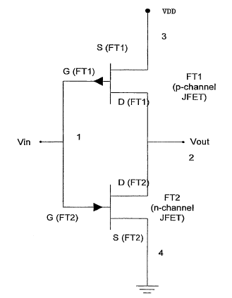
An exemplary circuit diagram of an inverter is shown in Figure 1. The
operating terminal voltages of the two transistors under ON and OFF conditions
are
shown in Table 1:
-9-
CA 02631032 2008-05-23
WO 2007/067684 PCT/US2006/046666
Table 1: Terminal Voltages at the CFET Gate Under ON and OFF Conditions.
Vin Vout FT1 FT2
0 Vdd ON OFF
Vdd 0 OFF ON
The operation of the circuit shown in Figure 1 can be remarkably similar to
the operation of the corresponding CMOS circuit. Exemplary embodiments of
JFETs described herein can operate at voltage levels which are similar to the
voltage levels of the known CMOS technology. The input voltage varies between
0
and Vdd. The output voltage varies between Vdd and 0 in an inverse
relationship to
the input voltage. Thus, for the two states of the inverter, when the applied
voltage
at the input terminal is 0 and Vdd, the output voltage is Vdd and zero
respectively.
This can be achieved by the two transistors FTl and FT2 being switched ON and
OFF, as stated in Table I above.
JFETs operate by applying a control signal at the gate, which controls the
conduction characteristics of the channel between the source and the drain.
The gate
forms a p-n junction with the channel. The voltage at the gate with respect to
the
source controls the width of the depletion region of the gate-to-channel
junction.
The undepleted part of the channel is available for conduction. Thus, the
channel is
turned ON and OFF by applying appropriate voltages at the gate and source
terminals of the JFET transistor. Current will flow between the source and the
drain
when the channel is turned ON and the appropriate voltage is applied to the
drain.
The JFET transistors FT1 and FT2 in the JFET inverter can function in a
manner very similar to the MOS transistors in a CMOS inverter. The operation
of a
CMOS inverter is well known to those skilled in the art. The p-channel JFET
(FT1)
is connected to the power supply at its source terminal. The n-channel JFET
(FT2)
is connected to the ground at its source terminal. The drain terminals of the
two
transistors are connected together and to the output terminal of the gate. The
gate of
the p-channel JFET FT1 and the gate of n-channel JFET FT2 are connected
together
and to the input terminal of the gate, as shown in Figure 1. This circuit
configuration is called a CFET inverter in the remainder of this document. In
-10-
CA 02631032 2008-05-23
WO 2007/067684 PCT/US2006/046666
general, gates formed in a similar manner with p-channel and n-channel JFETs
are
called CFET gates.
The functioning of the inverter is explained in greater detail here in order
to
reveal an exemplary full implementation. This is accomplished by first
explaining
the voltages at the source and the drain terminals of the transistor, which
are shown
in Table 2. In an exemplary and non-limiting illustration, the power supply
voltage
is fixed at 0.5V.
Table 2: Junction voltages for JFETs in CFET Gate
Vin Vout FTl FT2
VGS VDS VGS VDS
0.5 0 OV -0.5 0.5 0
0 0.5 -0.5 0 0 0.5
The gate of the p-channel JFET is made of n-type silicon and the channel is
doped p-type. The doping profile of the p-channel JFET is designed to turn off
conduction through the channel when the voltage on the gate terminal is at
zero volts
relative to the source terminal. This device is an enhancement mode device.
This
attribute of the p-channel JFET is due to the built-in potential at the p-n
junction
between the gate (p-type) and the channel (n-type). Since the source of the FT
1 is
tied to VDD at 0.5V, the external bias between the n-type channel and p-type
gate is
O.OV when the gate of the FT1 is also at 0.5 V. This represents the FT1 in the
OFF
condition. As the bias at the gate of the p-channel transistor is decreased to
O.OV,
the negative voltage between the gate and the source terminals changes to -
0.5V,
which causes the depletion layer to collapse and allows the flow of current
from
source to drain. This represents the FT 1 in the ON condition.
Exemplary embodiments can limit gate current when FTl is in the ON
condition. The channel-to-gate diode is forward biased at 0.5 V under this
condition, so there is a finite leakage current which flows through the gate
of the
transistor. It is termed the gate leakage. The magnitude of the gate leakage
is
controlled by the built-in potential across the gate - channel junction. The
built-in
potential limits the gate leakage current to a very small amount when this
CFET
-11-
CA 02631032 2008-05-23
WO 2007/067684 PCT/US2006/046666
inverter is operated with supply voltages (VDD) at or below 0.5V for silicon-
based
circuits. Thus, the CFET inverter works in a manner similar to the CMOS
inverter
in both design and operating characteristics. The limit for supply voltages
may be
different for other materials because of differences in the built-in
potential.
Similarly, the bias voltages for the n-channel JFET are reversed; the
transistor is
turned "OFF" when the gate - source bias is reduced to zero and it is turned
on when
the gate - source bias is equal to the supply voltage VDD, which is limited to
0.5V in
order to restrict the gate current. The gate current of a typical gate-channel
junction
is projected in the range of luA/cma to 100 mA/cm2. In contrast, for an MOS
transistor made with 45 nanometer lithography and appropriately scaled gate
dielctric thickness, the gate current is projected to be in excess of 1000
AJcm2.
The input capacitance of the JFET transistor is the junction capacitance of
the diode formed by the gate - channel terminals. The capacitance of this
diode is in
the range of 10-$ F/cm2 to 10"6 F/cm2 , determined by the thickness of the
depletion
layer width of the junction, which is in the range of 100 angstroms to 3000
angstroms. The input capacitance of an MOS transistor made with 45 nanometer
design rules and 10 angstrom thick oxide is an order of magnitude higher than
the
corresponding input capacitance of the JFET. This feature makes the JFET
extremely attractive from the perspective of low power operation.
The JFET transistors also have a fourth electrical terminal, namely the well.
One embodiment of the invention is described here with the well connected to
the
source terminal for both the JFETs, as shown in Figure 2a.
Figure 2b shows an alternate embodiment, in which the well is tied to the
gate and used for modulating the conductivity of the channel from both the top
and
the bottom.
Figure 2c shows yet another embodiment, in which the well of the n-channel
JFET is connected to an external terminal, which can be used for applying any
signal
to the JFET. In yet another embodiment, the well of the n-channel JFET is left
floating. The corresponding description also applies to the p-channel JFET. It
is
well known to those skilled in the art to measure power supply leakage current
as an
effective screen for detecting defects introduced in the fabrication of the
device.
This method is sometimes referred to as the Iddq test by those skilled in the
art. This
-12-
CA 02631032 2008-05-23
WO 2007/067684 PCT/US2006/046666
method is effective for CMOS with the minimum line width above 350 nm. Scaling
CMOS with the minimum line width below 350 nm increases the inherent leakage
current to be comparable to the defect induced leakage current, thus rendering
the
Iddq test ineffective. For MOS devices with the minimum line width below 100
nm,
biasing the well voltage of the MOS device to eliminate the inherent leakage
current
introduces new elements of leakage such as gate leakage, junction tunneling
leakage,
etc. In an exemplary embodiment, biasing the well voltage of the JFET can
effectively reduce the inherent leakage current to the pico-ampere range. This
makes the Iddq test an efffective screen for detecting defects introduced in
the
fabrication of devices with the minimum line width below 100 nm.
Figure 3a shows an exemplary and non-limiting layout of the JFET transistor
which is used to build this circuit structure. The source, drain, gate and
well tap of
the n-channel JFET are given by 330, 340, 375, and 368 respectively. The
contacts
to these terminals are marked by 372, 374, 373, and 371 respectively.
Figure 3b shows a cross-section of the structure of an n-channel JFET which
includes (e.g., consists of) four terminals; source (330), gate (370), drain
(340), and
p-well (310). The JFET is formed in a region of silicon marked as 315. The
JFET is
isolated from the surrounding semiconductor by regions marked as 320; these
are
filled with an insulating material such as silicon dioxide. The channel
between the
source and drain is shown as object 350. For the n-channel JFET, the source
and
drain are highly doped n-type regions formed by doping silicon with donor type
impurities such as phosphorous, arsenic or antimony. The well is doped by
acceptor
impurities such as boron or indium. The channel is a narrow region which is
doped
n-type connecting source and drain. The gate is a shallow p-type region 370
formed
within the channel by methods such as diffusion of dopants from the heavily p+
doped polysilicon region 375.
A doping profile of the transistor at varying depths from the silicon surface
through the gate (370) and channel (350) is shown in Figure 3c. The curve 381
is an
exemplary doping profile of the gate region starting from the silicon surface.
Curves
382, 383, and 384 represent the doping profile of the channel, well, and the
bulk
regions. For the n-JFET, 381 is the doping profile of the p-type gate region,
382 is
the profile of then-type channel region, 383 is the profile of the p-type well
region,
-13-
CA 02631032 2008-05-23
WO 2007/067684 PCT/US2006/046666
and 384 is the profile of the surrounding n-type bulk region. The gate -
channel
junction is given by 385, the channel - well junction is given by 386, and the
well -
bulk region junction is given by 387. The depth of the junction between gate
and
channel from the surface of silicon (385) is less than the depth of the
junction
between the channel and the p-well (386).
Other methods for forming the p-type gate junction, such as ion-implantation
are encompassed herein. Other methods to dope the gate, such as plasma
immersion
implant, as is well known to those skilled in the art, are also encompassed.
In Figure 3b, the Region 375 is a slab of polysilicon which is doped heavily
p-type and acts as the source for doping of the gate 370. The p - type gate is
used to
control the conduction across the channel from source to drain. By this novel
construction technique, the gate is diffused in the channel region from
heavily doped
polysilicon which also forms an ohmic contact with the gate. This allows the
polysilicon to be used to connect the gate to the external circuit.
The ohmic contact to the well is made by the well tap marked as object 368.
The contacts to the four terminals of the JFET, namely well, source, gate, and
drain
are shown in Figure 3b also, as objects 371, 372, 373, and 374, respectively.
The
region underneath the p-well tap 368 is doped heavily with p-type impurities
to
make good ohmic contact. The p-well 310 is formed in an n-well marked as 315
for
applications where the p-well of the JFET has to be isolated. For applications
where
the p-well is connected to the ground potential, the need for the n-well is
obviated.
Both of these cases are encompassed herein.
The doping types are reversed for the p-channel JFET in relation to those
described in Figure 3b and 3c, i.e. the p-type regions are replaced by n-type
regions
and vice versa. It should be pointed out that doping the gate of the JFET with
polycrystalline silicon 375. is maintained for the p-channel JFET also.
An alternate embodiment of the JFET is shown in Figure 4. This Figure
shows the cross section of an n-channel JFET, which is very similar to an MOS
transistor. The structure of the n-channel JFET is described here. It is
implied that
this structure will also be replicated for the p-channel JFET with appropriate
changes in doping, as described in the paragraph above. The JFET is shown as
object 400. The p-well in which the JFET is formed is marked as object 310.
The
- 14-
CA 02631032 2008-05-23
WO 2007/067684 PCT/US2006/046666
isolation for the JFET is provided by a region filled with an insulating
material such
as silicon dioxide or other suitable materials in object 320. This structure
is similar
to the corresponding structure shown in Figure 3. The heavily doped n-type
regions
form the source and drain region and are marked 420 and 430, respectively. The
channel region between source and drain is lightly doped n-type and is marked
450.
The gate region is doped p-type and is marked 440. This region is diffused
from the
polysilicon with heavy p-type doping marked as 460. An insulating region
marked
465 is inserted here, surrounding the gate, consisting of a combination of
silicon
dioxide and nitride layers. This object is called a "spacer" in this document.
In an
exemplary embodiment, top surfaces of the regions 420, 430, 460 and 368 are
covered with a highly conducting layer of one of the metallic compounds called
silicides, marked as 462. The silicide layer is self aligned to the well tap,
source,
drain, and gate regions, implying that the silicide is formed only in the
regions
where there is exposed silicon or polysilicon. An exemplary purpose served by
the
spacer is that it isolates the source and drain regions from the gate region
when self
aligned silicides are formed. It also allows efficient distribution of current
from the
contact inside the device. The contacts to the well tap, source, drain, and
gate
regions are done in a manner similar to that in Figure 3, and are marked as
371, 372,
373, and 374, respectively.
In an alternate embodiment of the JFET, as shown in Figure 5, contacts to all
the terminals of the JFET, namely source, gate, drain, and well, are all made
with
polysilicon. This structure has the desirable attribute of having contacts to
all
terminals at the same level. The n-channel JFET is made in a p-well marked 3
10,
which is isolated from all sides by an insulated region 320. This structure is
similar
to the corresponding structure shown in Figure 3. The source of the JFET is
formed
by a combination of heavily n-doped regions 520 and 522. The drain of the JFET
is
also formed by a combination of heavily doped n-type regions 524 and 526. The
channel 550 is a shallow n-type doped region between drain and source. The p-
type
gate region diffused in silicon is marked as 540. Blocks 530 and 532 are
heavily n-
type polysilicon doped regions. The region 520 is formed by diffusing n-type
impurities from the polysilicon into the silicon. Similarly, region 524 is
formed by
diffusion of n-type impurities from the polysilicon region 532 into the
silicon. The
-15-
CA 02631032 2008-05-23
WO 2007/067684 PCT/US2006/046666
gate region 540 is formed by diffusion of the p-type impurities from the p-
type
polysilicon 560 into the silicon. The regions 522 and 526 connect the source
and the
drain regions 520 and 524, respectively, to the channel 550. The polysilicon
regions
marked as 530, 532 and 560 are in ohmic contact with regions 520, 524, and 540
respectively. The regions 522 and 526 are formed by external doping such as
ion
implantation, plasma immersion implantation, or other similar doping methods.
The
well tap is formed by ohmic contact between the heavily p-doped polysilicon
562
and the p-type region 368. The contacts to the transistor are made at the top
of the
objects 530, 532 and 560 and 562. In order to reduce ohmic contact resistance
of
these regions, self aligned silicide is formed on top of the polysilicon
layer, marked
as 580. In an alternate embodiment , contacts to the terminals of the
transistor are
made directly to the polysilicon.
In an alternate embodiment, the top surface of the silicon substrate is formed
by epitaxial deposition of silicon-germanium alloy, which is doped
appropriately to
form the channel and the gate, shown in Figure 6. The structure is built-in a
well
310 with isolation regions 320. An exemplary feature of this embodiment is
that the
channel of the JFET is formed on an epitaxially deposited layer of silicon-
germanium alloy marked as object 670. The mobility of the silicon-germanium
alloy is much higher than silicon, which increases the performance of the
JFET,
especially at high frequencies. This epitaxial layer is deposited on the
transistor
after the formation of the isolation structure on the wafer. The epitaxial
layer can be
deposited selectively in this embodiment on the islands where the channel is
to be
formed. The epitaxial layer for the channel of the nJFET is deposited in one
step,
and the epitaxial layer for the channel of the pJFET is deposited in the next
step. In
another embodiment, the epitaxial layer is deposited on the wafer prior to the
formation of the isolation structure. In yet another embodiment, the channel
region
is formed by a strained silicon-germanium alloy_ Another embodiment teaches
the
use of silicon-germanium-carbon to build the channel region of the JFETs. The
terms silicon-germanium alloy and strained alloys are well known to those
skilled in
the art. The silicon-germanium alloy is formed by deposition of a mixture of
silicon
and germanium atoms epitaxially on the silicon substrate. The remaining
structure
of the JFET is similar to the structure shown in Figure 5. The doping of the
-16-
CA 02631032 2008-05-23
WO 2007/067684 PCT/US2006/046666
epitaxially deposited channel is controlled by external doping, such as ion
implantation. Alternately, the epitaxially deposited material is doped during
deposition by methods such as atomic layer epitaxy and similar techniques. The
epitaxial deposition steps are also applicable to the JFET structures shown in
Figure
3 and 4.
Another embodiment, shown in Figure 7, involves the use of a high band gap
material such as silicon carbide or silicon-germanium carbide to form the gate
contact region 744. This feature is implemented in order to increase the
barrier
height at the p-n junction formed at the gate 640 - channel 650 junction. The
high
band gap material of the gate contact region 744 in proximity to the gate
region 640
effectively increases the barrier height at the p-n junction formed at the
gate 640 -
channel 650 junction. The higher gate - channel junction built-in potential
reduces
the saturation current across the junction, and allows an increase in the
maximum
voltage which can be applied to the gate-channel diode to forward bias it
without
causing a significant amount of gate current to flow across the diode. Since
the
maximum voltage at the gate is equal to the power supply voltage of the
inverter, a
higher power supply voltage becomes possible, increasing the. drive strength
of the
transistors and resulting in faster switching of the inverter. As shown in
Figure 7 for
this embodiment, the polycrystalline silicon carbide material is used in place
of
polysilicon to form the electrodes. The use of a high band gap material such
as
polycrystalline silicon carbide reduces the leakage current of the gate
junction when
the gate-channel diode is weakly forward biased during the ON state of the
transistor. Various phases of silicon carbide can be used for this purpose,
namely
3C, 4H, and 6H. Further, various other electrode materials can be used to form
a
rectifying junction with the silicon substrate, including ternary alloys of
silicon -
germanium - carbon and various other compound semiconductors such as gallium -
aluminum - arsenide - phosphide. In an alternate embodiment, use of materials
for
the gate such as silicon carbide is made along with epitaxially deposited high
mobility materials such as silicon-germanium at the same time. The composition
of
the gate material is varied during deposition. The electrode extensions for
source,
drain, gate, and well tap, marked as 730, 732, 744, and 752, are made of high
band
gap semiconductor material such as silicon carbide. A self aligned conducting
layer
-17-
CA 02631032 2008-05-23
WO 2007/067684 PCT/US2006/046666
is formed on the top of these electrodes and is marked as 750. The
polycrystalline
semiconducting materials are doped appropriately, as described in the previous
paragraphs. The other components of the transistors remain similar to the
nJFET
structure described in Figure 6.
An exemplary embodiment teaches the use of a silicon-carbide layer near the
surface of the silicon to a depth ranging from lOA to 1000A, followed by
deposition
of polysilicon to a depth of l OA to 2500A. The composition of the
polycrystalline
layer is varied to facilitate accurate monitoring of the etching process, in
which the
polycrystalline material is etched fast until the composition marking the
bottom of
the layer is detected and then slowly with a selective etching process until
all the
polycrystalline material is etched. Detailed explanation of the fabrication
process
using polycrystalline silicon carbide is explained later in this document.
Next, an exemplary but non-limiting method of building the cotnplementary
3FET structure as shown in Figure 5 is illustrated as the flow chart in Figure
9. Each
step in the flow chart is further illustrated in Figures 10-20. Step 905 is
illustrated in
Figure 10. Step 910 is illustrated in Figure 11. Step 915 is illustrated in
Figure 12.
Step 920 and=925 are illustrated in Figure 13. Step 930 is illustrated in
Figure 14.
Step 935 is illustrated in Figure 15. Step 940 is illustrated in Figure 16.
Step 950 is
illustrated in Figure 17. Step 955 is illustrated in Figure 18. Step 960 is
illustrated
in Figure 19.- Step 965 is illustrated in Figure 20.
Figure 10 shows the cross sectional view of a semiconductor substrate after
the preliminary steps during the fabrication have been completed to achieve
the
isolation of the various regions where active devices will be formed by a
combination of etching, thermal oxidation and deposition of silicon dioxide.
Regions 1001 - 1005 represent the regions which are filled with insulating
material
comprises (e.g., consisting of) silicon oxide and nitride by a combination of
etching,
deposition and thermal growth. The details of the process for the formation of
these
regions are well known to those skilled in the art and are beyond the scope of
this
disclosure. Regions 1011 - 1014 represent regions where active transistors are
formed in the subsequent steps.
Figure 11 shows the formation of n-wells and p-wells by doping the active
regions with appropriate impuri-ties in regions 1101 and 1102. For the n-wells
in
-18-
CA 02631032 2008-05-23
WO 2007/067684 PCT/US2006/046666
region 1102, phosphorous or arsenic atoms are implanted. The doping level of
the
implant varies between 1.Ox1011 /cm2 to 1.Ox1014/cm2. The energy of
implantation
varies between 10 KeV and 400 KeV. For the p-wells in region 1101, boron is
introduced by ion implantation with a dose varying between 1.Ox10" /cm2 and
1.0x10¹⁴ /cm2 and with the energy of implantation varying between 10 KeV and
400
KeV. Multiple implants may be used to achieve the desired impurity doping prof
le.
In order to selectively implant regions with n-type and p-type impurities,
implants
are done using photoresist masks to shield the region not designed to receive
the
implant. Additional implants of boron are done under the isolation regions
1001 -
1005 to increase the doping in the region underneath the oxide and prevent any
leakage between the two adjoining n-wells. The wafers are heat-treated to
achieve
the desired impurity doping profile.
Figure 12a and 12b show the formation of channel regions 1202 for the
nJFET and 1222 for the pJFET respectively. The channel region is formed by
selective implantation using photoresist masks. For the nJFET, the channel is
formed by ion implantation with an n-type dopant such as arsenic, phosphorous,
or
antimony with an implant dose of 2.Ox1011/cm2 to 1.0x10¹⁴ /cma and with the
implant energy between 1 and 100 KeV, shown as region 1202 in Figure 12a. Also
shown in the Figure is the photoresist 1210 covering the regions where the n-
channel
implant is to be blocked. Region 1222 in Figure 12b is implanted with p-type
impurities such as boron, indium or thallium to form the channel of the pJFET.
In
an alternate embodiment, the channel region is formed by plasma immersion
doping.
Alternately, the channel is formed by epitaxial growth of the channel region
consisting of silicon, silicon - germanium binary alloys, or silicon -
germanium -
carbon tertiary alloys. Variations in formation of epitaxial regions by
selective
epitaxial growth of channel regions for n-channel and p-channel are
encompassed
herein., as well as a single deposition of the channel regions for both nJFET
and
pJFET, followed by selective doping. Yet another embodiment covers the
instance
in which the channel regions are doped during deposition by methods such as
atomic
layer epitaxy.
Next, a layer of polysilicon is deposited over the whole wafer, as shown in
Figure 13. The thickness of polysilicon deposited on the wafer varies between
100A
-19-
CA 02631032 2008-05-23
WO 2007/067684 PCT/US2006/046666
and 10,000A. The polysilicon is selectively doped to form regions which will
eventually become the source, drain, gate, and well contacts of the JFETs
using
photoresist as masks. The details of the photolithographic process are omitted
here
for the sake of brevity. As shown in 1300, the region marked as 1310 is doped
with
a heavy boron implant to a dose ranging between 1 x 10 13/cm2 and 1 x 10
16/cm2. It is
designed to act as the contact for the well region of the n-JFET. Region 1314
is
designed to act as the gate contact for the n-JFET. It is doped heavily p-type
with
the parameters similar to those of region 1310. Regions 1312 and 1316 are
doped
heavily with n-type dopants (phosphorous, arsenic, and antimony) to a dose
ranging
between 1x10¹³ /cmZ and 1x10¹⁶/cm2'
The p-JFET is formed with regions 1324 and 1320 acting as the source and
drain contacts (p type), respectively, region 1322 as the gate (n type), and
region
1326 as the contact to the well tap (n type). Regions 1320 and 1324 are doped
with
a heavy concentration of boron atoms to a dose ranging between 1x10¹³ /cm2 and
1 x 10 1 6/cm2 and are designed to act as the source and drain contacts of the
pJFET
respectively. Similarly, regions 1322 and 1326 are doped heavily n-type and
are
designed to act as gate and well contacts of pJFET. In an alternate
embodiment, a
layer of oxide is deposited on top of the polysilicon layer before doing the
ion
implantation. The thickness of this layer varies between 20A and 500A. In
another
embodiment, layers of oxide and nitride are deposited on top of the
polysilicon prior
to ion implantation, with the thickness of the oxide and nitride films varying
between I0A and 500A.
Figure 14 shows the cross section of the silicon wafer with the polysilicon
layer doped with impurities, and a protective layer 1410 on top of the
polysilicon
layer. The polysilicon layer with impurities implanted in various regions is
used as a
source of indirect diffusion of those impurities into the silicon to form the
source,
drain, and gate junctions and ohmic connections to the well. Regions 1422 and
1426
are the source and drain regions of the nJFET which are diffused from
polysilicon
regions 1312 and 1316. Region 1424 is the n-type channel. The gate region,
marked as 1428, is diffused into the silicon from the p-doped polysilicon.
Region
1420 is the p-type region (well tap) formed in the silicon by diffusion from
the
polysilicon region 1310 and forms an ohmic contact to the p-well which
contains the
-20-
CA 02631032 2008-05-23
WO 2007/067684 PCT/US2006/046666
nJFET. Similarly, the pJFET contacts in the silicon are formed by regions 1434
as
the source, 1432 as the channel, region 1430 as the drain, region 1436 as the
well
contact, and region 1438 as the gate region of the pJFET. In an alternate
embodiment, multiple ion implants, varying the implant dose and energy, of n-
type
and p-type dopants in polysilicon are made to form the well contacts, source,
drain,
and gate regions.
After diffusion of the various regions of the JFETs into the silicon, the gate
patterning process takes place. Using an optical lithographic process, a layer
of an
anti-reflective coating, followed by a layer of photoresist are coated on the
wafer.
The thickness of these layers depends upon the selection of the photoresist,
as is
known to those skilled in the art. The photoresist layer is exposed and
various
terminals are delineated in the photoresist, marked as 1510 in Figure 15.
Alternate
embodiment includes other methods of patterning the photoresist, including
imprint
lithography and e-beam lithography. With the photoresist layer as the mask,
the
protective layer above the polysilicon is etched first. Next, the polysilicon
layer is
etched, with the grooves such as 1512 reaching the bottom of the polysilicon
layer.
This step isolates the various terminals electrically, as shown in 1500. For
patterning the photoresist, various processes such as optical lithography,
immersion
lithography, imprint lithography, direct write e-beam lithography, x-ray
lithography,
or extreme ultraviolet lithography are used.
Figure 16a is the cross section of the silicon wafer after doping the link
region between the gate and the drain / source of the p-channel JFET. After
etching
the polysilicon layer, the region between the heavily doped regions and the
channel
are doped to form a low conductivity path between the source and channel, and
the
drain and channel. They are called the link regions 1620 and 1622 (see Figure
16a);
as well as 1652 and 1654 (see Figure 16b). Figure 16a further shows the
formation
of the link region for a pJFET. The section of the wafer containing the nJFET
is
covered by photoresist 1610 during this step while a suitable doping process
such as
ion implantation or plasma immersion implantation is used to dope the link
regions
of pJFET 1620 and 1622. The link regions are formed to a junction depth
independent from that of.the neighboring source and drain regions, and are
designed
to provide a very low resistivity connection between source / drain and the
channel.
-21-
CA 02631032 2008-05-23
WO 2007/067684 PCT/US2006/046666
Figure 16b is the cross section of the silicon wafer after doping the link
region between the gate and the drain / source of the n-channel JFET. Object
1650
is the photoresist covering the regions where the implant is blocked, which
contain
the pJFET. Regions 1652 and 1654 in the silicon are the link regions formed by
the
implantation of n-type dopants. After ion implantation, the dopants are
activated by
a rapid thermal annealing process. An oxidation step, at temperatures ranging
between 700C and 950C and for times ranging between 10 seconds and 20 minutes,
is also performed to oxidize the region of silicon damaged during etching.
Figure 17 shows the cross section of the wafer after the gap between the
polysilicon blocks is filled with an insulating material such as silicon
dioxide and
then processed, using a method such as chemical-mechanical-polishing, to
provide a
nearly planar surface at the same level as the polysilicon layer. The
technique of
filling insulating material in between the polysilicon blocks by depositing
silicon
dioxide using chemical vapor deposition or plasma assisted chemical vapor
deposition is one which is widely used in semiconductor manufacturing. One
such
process employs the deposition of oxide by a low temperature plasma-activated
reaction between silane and oxygen in gaseous form. The protective layer 1410
is
finally removed to expose the bare polysilicon surface.
Figure 18 is the cross section of the silicon wafer after formation of self
aligned silicide on the exposed polysilicon surfaces. A layer of a metal such
as
nickel, cobalt, titanium, platinum, palladium, or other refractory metal is
deposited
on the polysilicon surface and annealed such that the exposed regions of
polysilicon
form a binary compound with the metal layer known as "metal silicides". The
metal
silicide is a very highly conductive substance. An exemplary thickness of the
deposited metal is between 50A and 1000A on an atomically clean surface of
polysilicon. The wafers are heated in a rapid anneal furnace at temperatures
between 200C and 800C for a time period between 10 seconds and 30 minutes to
form silicides selectively where metal is in contact with a silicon or
polysilicon
layer. After the reaction between the metal layer and silicon has taken place,
the
excess metal is removed from the wafer by a chemical etching process which
does
not affect the silicide layer. Unreacted metal is selectively etched off using
appropriate solvents, leaving only metal silicide over the exposed silicon and
-22-
CA 02631032 2008-05-23
WO 2007/067684 PCT/US2006/046666
polysilicon regions 1801. For titanium and cobalt, a mixture of hydrogen
peroxide
and ammonium hydroxide is used in ratio of 1:0.1 to 1:10 as appropriate at
room
temperature, although temperatures above room temperatures can also be used.
Thus, a self aligned layer of silicide is formed on polysilicon. Figure 18
shows the
cross section of the device after formation of silicide on the polysilicon
source,
drain, gate, and well tap terminals. This polysilicon layer is also used as a
local
interconnect, whereby regions of silicided n-type polysilicon and p-type
polysilicon
are used for making ohmic contacts.
The next process step consists of depositing a dielectric (oxide) layer,
etching contact holes in the oxide layer, and forming contact holes for the
source,
drain, gate and well tap terminals, and continuing with the conventional metal
interconnect formation process as practiced in the formation of semiconductor
chips.
A cross section of the wafer after dielectric deposition and contact hole etch
is
shown in Figure 19. The metal deposition and etch is shown in Figure 20.
This process can be adapted for making MOS transistors along with JFETs.
One application of this adaptation is to include CMOS-compatible I/Os on the
chip.
The process to make MOS transistors is described next. Figure 21 shows the
cross
section of a wafer after the formation of the n-wells and p-wells for JFETs
and
MOSFETs. The threshold (Vt) adjust implants for the MOSFETs are also
completed. In addition, the formation of channel regions for the JFETs is also
completed. A layer of gate dielectric (oxide or nitrogenated oxide) is grown
on the
wafer. This layer of oxide is etched away from the wafer except in the regions
surrounding the gate of the MOSFETs. This oxide layer is shown as object 2110.
In
an alternate embodiment of this invention, a thin layer of amorphous silicon
is
deposited on top of the gate dielectric immediately after the oxide is grown.
The
thickness of this amorphous layer is sufficient to prevent damage to the
underlying
gate dielectric during the next photomasking and etching step. The preferred
thickness of this amorphous silicon layer is between l OA and 5000A. In an
alternate
embodiment of the invention, the oxide layer is formed first, and the channel
for the
JFETs is formed afterwards.
Next, a layer ofpolysilicon is deposited on the wafer as shown in Figure 22.
The polysilicon layer is covered by a protective layer of oxide marked as
2220.
-23-
CA 02631032 2008-05-23
WO 2007/067684 PCT/US2006/046666
With photolithography to define certain regions on the wafer, a layer of
photoresist
is selectively removed from the wafer and the exposed areas are implanted with
n-
type and p-type dopants. This Figure shows the polysilicon layer with
selectively
doped regions. Region 2210 is doped p-type, region 2212 is doped n-type,
region
2214 is doped p-type, and region 2216 is doped n-type. The parameters for
doping
these regions are the same as the parameters described in Figure 13.
The next step is the definition of the gate and the remaining electrodes on
polysilicon, as shown in Figure 23. It is accomplished by first defining the
pattern
in a photoresist layer 2330. Next, using the photoresist layer as a mask, the
polysilicon layer is etched to define the electrodes. Region 2310 forms the
well tap
of the NMOS, region 2312 forms the source of the NMOS, region 2314 forms the
gate of the NMOS, region 2316 forms the drain of the NMOS, region 2324 forms
the source of the PMOS, region 2322 forms the gate of the PMOS, region 2320
forms the drain region of the drain of the PMOS, and region 2326 forms the
well tap
for the PMOS. After etching the polysilicon layer, a short oxidation cycle is
executed to form an oxide on the surface of silicon with a thickness between
20A
and 500A. Additional heat cycles are executed to diffuse the dopants into the
silicon
from the polysilicon in the drain, source, and the well tap regions while
controlling
the diffusion of the dopants from the polysilicon into the gate dielectric and
into the
channel region.
Figure 24 shows the formation of the link between the source, drain, and
channel regions by ion implantation. For NMOS, the links between the drain and
the channel and the source and the channel are formed by ion implantation of n-
type
dopants marked as 2410 and 2412 respectively. For PMOS, the links between the
source and the channel and the drain and the channel are formed by ion
implantation
of p-type dopants marked as 2420 and 2422 respectively. A rapid thermal anneal
is
carried out to activate the implant. The cross section of the wafer is very
similar to
the one shown in Figure 17. The wafer is processed by the method described in
Figures 17 through 20.
The complete flow for forming JFETs and MOSFETs on the same wafer is
shown in Figure 25. The MOS transistors fabricated in this manner can have
advantages over the known methods of building MOS transistors, as described
here:
-24-
CA 02631032 2008-05-23
WO 2007/067684 PCT/US2006/046666
Known MOS transistors have a spacer which is used to separate the highly
doped source / drain regions from the gate. The dimensions of the spacer are
dependent upon the vertical polysilicon dimension and other processing
parameters,
and are not laterally scalable. The current embodiment of the MOS transistor
uses
lithography to separate the source / drain and the gate region, making this
structure
laterally scalable.
Known MOS transistors have a lightly doped source and drain region under
the spacer, which limits the injection efficiency of the source, or the
maximum
current which can be controlled by the transistor. The current embodiment of
the
MOS transistor uses the link region as the source and drain junctions and it
allows
the doping of this region to be controlled independently.
Known MOS transistors have symmetrical source and drain regions. This
embodiment allows asymmetrical source and drain junctions to be formed by
spacing the source and drain polysilicon contacts from the gate
asymmetrically.
Known MOS transistors have varying contact depths to the source / drain
and the gate terminals; the contacts to the source / drain terminals are made
directly
to silicon while the contact to the gate terminal is made to polysilicon which
is
elevated from the source / drain junctions. This embodiment of MOS transistors
etches all the contact holes to the polysilicon, keeping the depth of all the
holes the
same.
Known MOS transistors compromise the short channel performance due to
limitations imposed by a shallow source / drain junction and the silicide
formation
on top of these junctions. This embodiment of the MOS transistors removes this
limitation by placing the silicide on top of the polysilicon for all the
junctions. Also,
the shallow source / drain junction in the silicon is formed by diffusion of
dopants
from the polysilicon, which is a slower and more controllable process.
This method to build JFETs and MOSFETs allows a planar surface to exist
prior to contact hole etch. It also insures that the amount of polysilicon
removed is
limited, which can be important in achieving a uniform plasma etch. It is well
known that the variation in the density of the polysilicon pattern on the
silicon wafer
is responsible for variation in the etch rate of polysilicon. In this method,
this
problem can be overcome by.the fact that the pattern density of polysilicon is
much
- 25 -
CA 02631032 2008-05-23
WO 2007/067684 PCT/US2006/046666
higher than in conventional process technology. Also, the contacts to the
various
junctions are separated by the polysilicon layer, which makes it extremely
convenient to form shallow,source and drain junctions.
Steps in Figure 25 are further illustrated in Figure 26 - 30.
Figure 26 shows the cross section of a silicon wafer after the formation of
isolation areas (2610), a p-well for forming NMOS transistors marked as 2601
and
another p-well for forming nJFETs marked as 2602. Corresponding well
structures
to form PMOS transistors and pJFETs are also formed but are omitted here for
the
sake of brevity. After the Vt adjust implants are performed in silicon for the
MOS
transistors, gate oxidation is performed over the whole wafer and a gate
dielectric
layer of appropriate thickness is grown on the wafer, ranging between 10A and
I OOA. It is shown as layer 2620 in this Figure. In alternate embodiments of
the
invention, the gate dielectric is formed with a high dielectric coefficient
material
such as hafnium silicate and similar materials known to those skilled in the
art.
Figure 27 shows the wafer cross section after the following steps have been
executed. First, the gate dielectric is removed by wet etching or a suitable
technique
such as plasma etching selectively from the regions where the JFET channel is
to be
formed. Next, the JFET channel is formed by ion implantation, marked as object
2710. After the formation of the channel, a layer of polycrystalline material
is
deposited on the wafer. It is marked as 2720.
The gate electrodes of the JFET and the MOS transistors are implanted with
appropriate dopants. The gate regions of the NMOS transistor and the pJFET are
doped heavily n-type with arsenic, phosphorus, or antimony. The gate electrode
regions of the PMOS and the nJFET are implanted with p-type dopants, namely
boron. The gate electrode regions are implanted with a heavy dose of the
dopants in
the range of lx1014 /cm2 to 1x10¹⁶ /cm2. An alternate embodiment of the
invention
includes multiple implant steps for forming the gate electrode region of the
MOS
and JFET transistors. The wafer is heated to distribute the dopants throughout
the
polysilicon layer.
A photomask is put on the wafer and the layer of polysilicon is etched to
define the gate electrodes for the transistors, as is shown in Figure 28.
Object 2810
forms the gate of the NMOS transistor while the object 2820 forms the gate
-26-
CA 02631032 2008-05-23
WO 2007/067684 PCT/US2006/046666
electrode of the nJFET transistor. The gate of the NMOS transistor is formed
with
n-type polysilicon while the gate of the nJFET is formed with p-type
polysilicon.
After defining the gate, a short oxidation cycle is executed to remove the
damage
from the surface of polysilicon. Layers of oxide and nitride are deposited
next and
etched anisotropically to form spacers adjacent to the gate electrodes. At the
end of
the spacer formation, the cross section of the wafer shows a gate electrode
surrounded by spacers on both sides. The objects marked 2830 are the spacers
surrounding the gate. It should be noted here that the polysilicon on the
nJFET
islands (object 2602) does not have a layer of oxide underneath to stop the
etch. So,
the polysilicon etching process has to be conducted very carefully so as not
to over-
etch the polysilicon and etch into the silicon. Process steps to prevent over-
etching
the polysilicon have been described earlier in this application.
Figure 29 shows the cross section of the silicon wafer after the source and
drain regions for the MOS and JFET transistors are formed. The process step
consists of forming the Lightly Doped Drain (LDD) region for the NMOS
transistors. This is done by selective ion implantation of n-type dopants in
the
NMOS region 2601. This step is also accompanied with an implant of dopant of
opposite polarity (p-type) to prevent the depletion regions of drain and
source from
touching each other, causing a phenomenon known as "punch through". This step
is
known as the "anti-punch-through" implant. The LDD and the anti-punch-through
implants are performed at angle of incidence on the wafer ranging from
perfectly
vertical to a tilt of 60% from the vertical. These regions are marked as 2910
in the
Figure 29. A similar process is performed to create a low resistance region
(link)
between the channel of the JFET and the source and drain regions. The links
are
formed adjacent to the gate of the JFET, marked as objects 2920. The source
and
drain regions are formed by ion implantation of n-type impurities for both
NMOS
and nJFET transistors. The n-type ion implantation to form source and drain
terminals for NMOS is a well established process. For the nJFET, the doping
type
of source and drain is opposite to that of the gate. The implant parameters of
the
source and drain are adjusted to insure that the n-type dopants used for
forming
these terminals do not invert the polarity of the gate region. The gate doping
for the
JFET is maintained at a high level by implanting with n or p type dopants to a
dose
-27-
CA 02631032 2008-05-23
WO 2007/067684 PCT/US2006/046666
of 1x10¹⁴ / cma to 1x10¹⁶ / cmz. The energy of the implantation is selected
based on
the polysilicon thickness. The doping of the source and drain of the JFET is
kept
lower than the gate doping in order to insure that inversion of the gate
doping does
not occur. The source and drain regions of the NMOS transistor are marked as
2950
and 2952, and the source and drain of the nJFET are marked as 2954 and 2956,
respectively.
Figure 30a shows the cross section of the silicon wafer after contact holes
and metal connections are formed. Following the source and drain formation,
the
self aligned silicide formation takes place by depositing a layer of metal
such as
cobalt, nickel, titanium, platinum, etc. and heating the wafer to allow the
metal to
react with the exposed silicon surface, forming the silicide compound. The
unused
metal is washed away by a wet chemical etch. This is followed by deposition of
a
layer of oxide at temperatures below 600C as a dielectric layer to cover the
whole
wafer, as shown in Figure 30a. Contact holes 3010 are etched in the dielectric
layer.
Metallic alloys in single or multiple layers are deposited over the wafer and
they are
pattemed by a photolithographic process, followed by etching of the metal
layer to
form interconnects from the transistors shown as object 3020. The layout of
the
NMOS and nJFET is shown in Figure 30b. The source, drain, and gate regions of
the NMOS transistor are marked as 3051 and 3050, and 3054.. Their respective
contact holes are marked as 3060, 3061 and 3064. Similarly, source, drain, and
gate
regions of the nJFET are marked as objects 3052, 3053, and,3055, and their
contact
holes are marked as 3062, 3063, and 3065, respectively.
Exemplary embodiments provide numerous advantages described herein.
For example, compatibility with MOS can be achieved in accordance with
exemplary embodiments. An exemplary comparison of NFET and NMOS is shown
below. This is based upon Tox of 10 A for MOS; and TdePi,fioõ of 720 A for
JFET
(with corresponding channel doping 1 x 10¹⁸/cm2). This result in significant
in input
capacitance and related performance specifications, as shown in Table 1.
-28-
CA 02631032 2008-05-23
WO 2007/067684 PCT/US2006/046666
Table 1
NFET NMOS
Ldrawn 45nm 45
Ion (uA/um) 280 500
C* (fF) 0.06 1.5
CV/I** (pS) 0.27 3.1
'/aCV2 (W) 8.10E-18 7.77E-16
The gate region can have an impurity concentration doped from the gate
electrode region.
In comparison to fabricating a MOS structure, the JFET structure can be
manufactured with fewer processing steps. In addition to the elimination of
the gate
dielectric, the gate in a JFET can be fabricated by diffusing the dopants from
polysilicon. Using a single critical masking step and simplified contact hole
etch
process (i.e., drop down to the same level), process complexity can be
reduced.
Furthermore, electron mobility enhancing technology developed for CMOS (e.g.,
strained lattice) can be applicable to the JFET devices disclosed herein.
In exemplary embodiments, the thickness of the depletion layer can be
between about 100 A to about 3000 A during the application of the second
voltage.
The gate region can have a line-width of about 45 nm.
In an exemplary embodiment, a first JFET can be configured adjacent to a
second JFET, wherein the channel region of the first JFET is n-type and the
channel
region of the -second JFET is p-type. Figure 31 is an exemplary complementary
FET
(CFET), fabricated from two adjacent JFET devices previously described and
embodied in Figures 3b and 5. Figure 31 illustrates two adjacent device JFET
devices, one with an n-type channel and the other with a p-type channel.
-29-
CA 02631032 2008-05-23
WO 2007/067684 PCT/US2006/046666
Various devices currently utilize CMOS technology, for example, static logic
gates, dynamic logic gates, pass logic gates and memories. These devices can
be
fabricated by incorporating JFET technology as described herein. The JFET can
be
incorporated into any nuinber of circuits and/or devices including, but not
limited to
a memory device such as an SRAM.
Figure 32 shows an equivalent circuit to model the delay propagation delay
associated with an exemplary repeater insertion configured using a JFET
transistor
as described in H.B. Bakoglu, Ph.D. Dissertation, Stanford University 1986,
pp.
43-46.
In general, JFET devices with lower junction capacitance can reduce the
propagation delay, in comparison to their CMOS counterparts. Propagation
delay,
Td, can be computed from the following expression:
Td = k[2.3 Ro C' ' + hCo) + R i ' (C i ' + 2.3hCo)]
h k k k
By setting dTd/h=0 and dTd/dk=0, yields:
T d = 7.6 (RoR int CoC int)
or.
Td = Const. RoCo
In other words, the RoCo value for CFET exhibits an approximately ten-fold
decrease
or about a three-fold decrease in propagation delay.
Figures 33 and 34 illustrate the propagation delay, in seconds, as a function
of number of line segments k, and buffer segments, for both CFET and CMOS
devices.
Furthermore, assuming:
R Ii.t* C im
k=
Ro*Co
h Ro*Ci.c
R i.c* Co
Powet'='ZCim TYdd' +k*h*y*Co*V'dd2
-30-
CA 02631032 2008-05-23
WO 2007/067684 PCT/US2006/046666
and by substituting the expression for k and h into the expression describing
power
yields:
Power =/C int* Ydd Z+ Y2 2.3 * C int* Vdd a
Thus, at optimal values of k and h, power is a function of C,,,t only. In
other words,
power is independent of Co. The above expressions are also described, by H.B.
Bakoglu, Ph.D. Dissertation, Stanford University 1986, pp. 43 - 46,
incorporated by
reference in its entirety.
The following Table illustrates exemplary parameters of a CFET device
versus those of a CMOS device for use in the exemplary Figure 32 repeater:
45 nm Technology Node CFET CMOS
Global Wiring Line length (cm) 1 1
int S2 1.11 E+04 1:11 E+04
Cint F 1.57E-12 1.57E-12
0- Driver resistance 92- m 5.38E+02 3_ 14E+02
CO - Driver Input Capacitance
F/ m 6.48E-17 1.55E-15
- Optimum buffer width m 34.3 .5.3
k- O timum No. of segments 66.8 124.8
DD V 0.5 1
In alternate embodiments, where a plurality of JFET devices are configured
in a repeater chain, a propagation delay is inversely proportional to a number
of
devices in the requester chain. In one example, the propagation delay can be
less
than 20 nanoseconds. Such a feature is illustrated in the Figure 33 graph.
In alternate embodiments of a JFET device described herein, the channel
region can include at least a layer of strained material. For example, the
strained
material can be a strained silicon.
The semiconductor substrate can be formed of at least one of Si, GaAs, InP
or any III-V material.
-31-
CA 02631032 2008-05-23
WO 2007/067684 PCT/US2006/046666
An advantage of an NFET device as described herein is reduced leakage
current, in comparison to its NMOS counterpart, as illustrated in Figures 35
and 36.
The total leakage current is a sum of the following components: the sub-
threshold
current (ISUb), the gate current (Ig) and junction tunneling current (It).
Transistors as described herein can, for example, be suitable for next
generation telephone/PDA handsets having exemplary specifications as follows:
= Power = 0.1 W (idle) / 5W (active)
= Chip area = I cm2
= Gate count = 100 M
= ' Clock = 1 GHz
= 10% of the gates active at any time
= Power per gate = 500 nW
= 50% of the power dissipated as active power
= Active power = 250 nW = V2CV2
Fabrication of handsets with CMOS devices involve the following exemplary
characteristics: Vdd = 1.0 V, C = 0.5 fF/gate and Cgate = 1.5 fF/ m (state of
the art).
In contrast, exemplary fabrication of handsets with CFET, can be implemented
with
the following exemplary characteristics: Vdd = 0.5 V, C = 2.0 fF/gate and
Cga,e =
0.06 fF/ m (state of the art).
The following illustrates exemplary parameters of a next generation handset:
= Chip area = 1 cm2
= Gate count = 100 M
= Clock = 1GHz
= 10% of the gates active at any time
- Active power ='/2CV2*f*Nea, with f is as clock frequency, N as
total number of gates, and a is activity factor
= Ctotai / gate =3o co+$*He cint
- H is the cell height (=20F, feature size)
- C. is the input gate capacitance
- Cim is the wire capacitance/micron (0.15 fF/ m)
100M gates as configured with JFET transistors described herein can occupy 1
cm2,
where 1 gate occupies 1 um2, the feature size = 0.045nm and cell height H=
22F.
Applying these parameters, a CMOS chip with Vdd = 1.0 V, Ctotai = 4.79 fF
consumes 24.0 W of power. In contrast, a JFET chip as described herein with
Vdd =
0.5 V, Qotal = 1.63 fF consumes 2.0 W of power or exhibits a ten-fold decrease
in
-32-
CA 02631032 2008-05-23
WO 2007/067684 PCT/US2006/046666
power consumption. This beneficial characteristic can result in lower power
dissipation and low chip/package temperature effects, and low leakage.
As illustrated in Figures 37 and 38, for CMOS devices, the primary focus is
on the fabrication of devices with the emphasis on performance, while
minimizing
area, rather than power consumption. However, the primary focus of JFET
devices
includes low power consumption, while maintaining an emphasis on performance
and the minimization of area.
It will be appreciated by those skilled in the art that the present invention
can
be embodied in other specific forms without departing from the spirit or
essential
characteristics thereof. The presently disclosed embodiments are therefore
considered in all respects to be illustrative and not restricted. The scope of
the
invention is indicated by the appended claims rather than the foregoing
description
and all changes that come within the meaning and range and equivalence thereof
are
intended to be embraced therein.
- 33 -