Note: Descriptions are shown in the official language in which they were submitted.
CA 02631454 2008-05-28
WO 2007/076029 PCT/US2006/049063
1
LOW ENERGY, LONG LIFE MICRO-FLUID EJECTION DEVICE
FIELD OF THE DISCLOSURE:
The disclosure relates to micro-fluid ejection devices and in one particular
embodiment, to low energy, long life devices for ejecting small liquid
droplets.
BACKGROUND AND SUMMARY:
Micro-fluid ejection devices are classified by a mechanism used to eject
fluid.
Two of the major types of micro-fluid ejection devices include thermal
actuators and
piezoelectric actuators. Thermal actuators rely on an ability to heat the
fluid to a
nucleation temperature wherein a gas bubble is formed that expels the fluid
through a
nozzle. The life of such thermal actuators is dependent on a number of factors
including, but not limited to, dielectric breakdown, corrosion, fatigue,
electromigration, contamination, thermal mismatch, electro static discharge,
material
compatibility, delamination, and humidity, to name a few. A heater resistor
used in a
micro-fluid ejection device may be exposed to all of these failure mechanisms.
For example, it is well-known that cavitation pressures are powerful enough to
pound thru any solid material, from concrete dams to ship propellers.. During
each
fire cycle, the heater resistor may be exposed to similar cavitation impacts.
As the gas
bubble collapses, a local pressure is generated on the order of 103 to 104
atmospheres.
Such cavitation impacts may be focused on a submicron spot of the heater
resistor for
several nanoseconds. After 107 to 10$ cavitation impacts, the heater resistor
may fail
due to mechanical erosion. Furthermore, because the heater resistor requires
extremely high temperatures to ensure homogeneous bubble nucleation, a
distortion
energy in the heater due to thermal expansion may be generated of the same
order of
magnitude as the distortion *energy imposed by bubble collapse. A combination
of
thermal expansion and cavitation impacts may lead to premature heater failure.
In order to protect the fragile heater resistor films, the films may be
hermitically sealed to prevent humidity driven corrosion, but the surface of
the heater
resistor is directly exposed to liquid. In the most critical areas of the
heater, a minor
surface opening due to defect, wear, step coverage, or delamination may lead
to
catastrophic failure of the heater resistor.
CA 02631454 2008-05-28
WO 2007/076029 PCT/US2006/049063
2
Accordingly, exotic resistor films and multiple protective layers providing a
heater stack are used to provide heater resistors robust enough to withstand
the
cavitation and thermal expansion abuses described above. However, the overall
thickness of the heater stack should be minimized because input energy is a
linear
function of heater stack thickness. In order to provide competitive actuator
devices
from a power dissipation and production throughput perspective, the heater
stack
should not be arbitrarily thickened to mitigate the cavitation effects,
overcome step
coverage issues, overcome delamination problems, reduce electro static
discharge,
etc. In other words, improved heater resistor reliability by over-design of
the thin film
resistive and protective layers may produce a noncompetitive product.
Micro-fluid ejection heads may be classified as permanent, semi-permanent or
disposable. The protective films used on the heater resistors of disposable
micro-fluid
ejection heads need only survive until the fluid in the attached fluid
cartridges is
exhausted. Installation of a fluid cartridge carries with it the installation
of a new
micro-fluid ejection head. A more difficult problem of heater resistor life is
presented
for permanent or semi-permanent micro-fluid ejection heads. There is a need,
therefore, for a method and apparatus for improving heater resistor life
without
sacrificing jetting metrics and power consumption.
With regard to the above, exemplary embodiments of the disclosure provide
micro-fluid ejection heads having extended life and relatively low energy
consumption and methods of making a micro-fluid ejection heads with extended
life
and relatively low energy consumption. One such micro-fluid ejection head
includes
a substrate having a plurality of thermal ejection actuators disposed thereon.
Each of
the thermal ejection actuators includes a resistive layer and a protective
layer for
protecting a surface of the resistive layer. The resistive layer and the
protective layer
together define an actuator stack thickness. A flow feature member is adjacent
(e.g.,
attached to) the substrate and defines a fluid feed channel, a fluid chamber
associated
with at least one of the thermal ejection actuators and in flow communication
with the
fluid feed channel, and a nozzle. The nozzle is offset to a side of the fluid
chamber
opposite the fluid feed channel. A polymeric layer having a degradation
temperature
of less than about 400 C. overlaps a portion of the at least one thermal
ejection
CA 02631454 2008-05-28
WO 2007/076029 PCT/US2006/049063
3
actuator, and positioned less than about five microns from at least an edge of
the at
least one actuator opposite the fluid feed channel.
In another embodiment there is provided a method for extending a life of a
thermal ejection actuator for a micro-fluid ejection =head. A substrate has a
plurality
of thermal ejection actuators and a protective layer therefor deposited
thereon, and has
a flow feature member defining a fluid feed channel, a fluid chamber
associated with
at least one of the thermal ejection actuators and in flow communication with
the fluid
feed channel, and a nozzle. The nozzle is offset to a side of the fluid
chamber distal
from the fluid feed channel. The method comprises depositing a polymeric layer
having a degradation temperature of less than about 400 C. in overlapping
relationship with at least a portion of the at least one thermal ejection
actuator. The
polymeric layer overlaps less than about five microns of the at least one
actuator
adjacent an edge thereof distal from the fluid feed channel.
An advantage of at least some of the exemplary embodiments of the disclosure
is that heater energy is not increased while the life of the actuators is
substantially
enhanced. Another potential advantage of at least some of the disclosed
embodiments is an ability to vary the life of an ejection actuator without
significantly
changing the energy requirements for ejecting fluids.
BRIEF DESCRIPTION OF THE DRAWINGS
Further advantages of the embodiments will become apparent by reference to
the detailed description of exemplary embodiments when considered in
conjunction
with the drawings, wherein like reference characters designate like or similar
elements
throughout the several drawings as follows:
FIG. I is a cross-sectional view, not to scale, of a portiori of a prior art
micro-
fluid ejection head;
FIG. 2 is a graphical representation of jetting energy versus protective layer
thickness for micro-fluid ejection heads;
FIG. 3 is photomicrograph plan view of a prior art micro-fluid ejection
actuator having cavitation damage thereon;
CA 02631454 2008-05-28
WO 2007/076029 PCT/US2006/049063
4
FIG. 4 is a photomicrograph cross-sectional view of a prior art micro-fluid
ejection actuator having cavitation damage thereon;
FIG. 5 is a plan view, not to scale, of a portion of a prior art micro-fluid
ejection head;
FIG. 6 is a cross-sectional view, not to scale, of a portion of a micro-fluid
ejection head according to a first embodiment of the disclosure;
FIG. 7 is a plan view, not to scale, of a portion of a micro-fluid ejection
head
according to the first embodiment of the disclosure;
FIG. 8 is temperature profile for a micro-fluid ejection actuator according to
the disclosure;
FIG. 9 is a cross-sectional view, not to scale, of a portion of a micro-fluid
ejection head according.to a second embodiment of the disclosure;
FIG. 10 is a plan view, not to scale, of a portion of a micro-fluid ejection
head
according to the second embodiment of the disclosure; and
FIG. 11 is a perspective view, not to scale, of a fluid cartridge for a micro-
fluid ejection head according to the disclosure.
DETAILED DESCRIPTION OF EXEMPLARY EMBODIMENTS
In accordance with embodiments described herein, micro-fluid ejection heads
having improved energy consumption and extended life will now be described.
For the purposes of this disclosure, the terms "heater stack", "ejector
stack",
and "actuator stack" are intended to refer to an ejection actuator having a
combined
layer thickness of a resistive material layer and passivation or protection
material
layer. The passivation or protection material layer is applied to a surface of
the
resistive material layer to protect the actuator from, for example, chemical
or
mechanical corrosion or erosion effects of fluids ejected by the micro-fluid
ejection
device.
In order to more fully appreciate the benefits of the exemplary embodiments,
reference is first made to FIG. 1, which is a cross-sectional view, not to
scale, of a
portion of a prior art micro-fluid ejection head 10. The cross-sectional view
of FIG.1
shows one of many micro-fluid ejection actuators 12 contained on a micro-fluid
CA 02631454 2008-05-28
WO 2007/076029 PCT/US2006/049063
ejection head. The ejection actuators 12 are formed on a substrate 14. The
substrate
14 may be made from a wide variety of materials including plastics, ceramics,
glass,
silicon, semiconductor material, and the like. In the case of a semiconductor
material
substrate, a thermal insulating layer 16 is applied to the substrate between
the
5 substrate 14 and the ejection actuators 12. The ejection actuators 12 may be
formed
from an electrically resistive material layer 18, such as TaAI, Ta2N,
TaAl(O,N),
TaAISi; TaSiC, Ti(N,O), WSi(O,N), TaA1N, and TaAI/Ta. The thickness of the
resistive material layer 18 may range from about 300 to about 1000 Angstroms.
The thermal insulation layer 16 may be formed from a thin layer of silicon
dioxide and/or doped silicon glass overlying the relatively thick substrate
14. The
total thickness of the thermal insulation layer 16 may range from about 1 to
about 3
microns thick. The underlying substrate 14 may have a thickness ranging from
about
0.2 to about 0.8 millimeters thick.
A protective layer 20 overlies the micro-fluid ejection actuators 12. The
protective layer 20 may be a single material layer or a combination of several
material
layers. In the illustration in FIG. l, the protective layer 20 includes a
first passivation
layer 22, a second passivation layer 24, and a cavitation layer 26. The
protective layer
is effective to prevent the fluid or other contaminants from adversely
affecting the
operation and electrical properties of the fluid ejection actuators 12 and
provides
20 protection from mechanical abrasion or shock from fluid bubble collapse.
The first passivation layer 22 may be formed from a dielectric material, such
as silicon nitride, or silicon doped diamond-like carbon (Si-DLC) having a
thickness
ranging from about 1000 to about 3200 Angstroms thick. The second passivation
layer 24 may also be formed from a dielectric material, such as silicon
carbide, silicon
nitride, or silicon-doped diamond-like carbon (Si-DLC) having a thickness
ranging
from about 500 to about 1500 Angstroms thick. The combined thickness of the
first
and second passivation layers 22 and 24 typically ranges from about 1000 to
about
5000 Angstroms.
The cavitation layer 26 is typically formed from tantalum having a thickness
greater than about 500 Angstroms thick. The cavitation layer 26 may also be
made of
TaB, Ti, TiW, TiN, WSi, or any other material with a similar thernn.al
capacitance and
CA 02631454 2008-05-28
WO 2007/076029 PCT/US2006/049063
6
relatively high hardness. The maximum thickness of the cavitation layer 26 is
such
that the total thickness of protective layer 20 is less than about 7200
Angstroms thick.
The total thickness of the protective layer 20 is defined as a distance from a
top
surface 28 of the resistive material layer 18 to an outermost surface 30 of
the
protective layer 20. An ejector stack thickness 32 is defined as the combined
thickness of layers 18 and 20.
The ejection actuator 12 is defined by depositing and etching a metal
conductive layer 34 on the resistive layer 18 to provide power and ground
conductors
34A and 34B as illustrated in FIG. 1. The conductive layer 34 is typically
selected
from conductive metals, including but not limited to, gold, aluminum, silver,
copper,
and the like and has a thickness ranging from about 4,000 to about 15,000
Angstroms.
Overlying the power and ground conductors 34A and 34B is another
insulating layer or dielectric layer 36 typically composed of epoxy
photoresist
materials, polyimide materials, silicon nitride, silicon carbide, silicon
dioxide, spun-
on-glass (SOG), laminated polymer and the like. The insulating layer 36 and
has a
thickness ranging from about 5,000 to about 20,000 Angstroms and provides
insulation between a second metal layer and conductive layer 34 and corrosion
protection of the conductive layer 34.
Layers 14, 16, 18, 20, 34, and 36 provide a semiconductor substrate 40 for use
in the micro-fluid ejection head 10. A nozzle plate 42 is adjacent (e.g.,
attached, as by
an adhesive 44 to) the semiconductor substrate 40. In the prior art embodiment
illustrated in FIG. 1, the nozzle plate 42 contains nozzles 46 corresponding
to
respective ones of the plurality of ejection actuators 12. During a fluid
ejection
operation, a fluid in fluid chamber 48 is heated by the ejection actuators 12
to a
nucleation temperature of about 325 C. to form a fluid bubble which expels
fluid
from the fluid chamber 48 through the nozzles 46. A fluid supply channel 50
provides fluid to the fluid chamber 48.
One disadvantage of the micro-fluid ejection head 10 described above is that
the multiplicity of protective layers 20 within the micro-fluid ejection head
10
increases the ejection stack thickness 32, thereby increasing an overall
jetting energy
required to eject a drop of fluid through the nozzles 46.
CA 02631454 2008-05-28
WO 2007/076029 PCT/US2006/049063
7
Upon activation of the ejection actuator 12, some of the energy ends up as
waste heat energy used to heat the protective layer 20 via conduction, while
the
remainder of the energy is used to heat the fluid adjacent the surface 30 of
the
cavitation layer 26. When the surface 30 reaches a fluid superheat limit, a
vapor
bubble is formed. Once the vapor bubble is formed, the fluid is thermally
disconnected from the surface 30. Accordingly, the vapor bubble prevents
further
thermal energy transfer to the fluid.
It is the thermal energy transferred into the fluid, prior to bubble
formation,
that drives the liquid-vapor change of state of the fluid. Since thermal
energy must
pass through the protective layer 20 before heating the fluid, the protective
layer 20 is
also heated. It takes a finite amount of energy to heat the protective layer
20. The
amount of energy required to heat the protective layer 20 is directly
proportional to
the thickness of the protective layer 20 and the thickness of the resistive
layer 18. An
illustrative example of the relationship between the protective layer 20
thickness and
jetting energy requirement for a specific ejection actuator 12 size is shown
in FIG. 2.
Jetting energy is related to power (power being the product of energy and
firing frequency of the micro-fluid ejection actuators 12). The temperature
rise
experienced by the substrate 40 is also related to power. Adequate jetting
performance and fluid characteristics, such as print quality in the case of an
ink
ejection device, are related to the temperature rise of the substrate 40.
For disposable micro-fluid ejection heads, the thickness of the protective
layer
20 may be minimized in order to reduce power consumption. However, for longer
life micro-fluid ejection heads, such as permanent or semi-permanent ejection
heads,
increasing the protective layer 20 thickness to extend the life of the
ejection heads
may adversely affect the power consumption of the ejection heads as described
above.
For example, a disposable ejection head may provide up to about 10 million
ejection
cycles before failure of the ejection head. However, longer life ejection
heads may
require up to I billion ejection cycles or more before failure. Accordingly,
methods
and apparatus for extending the life of the ejection heads without adversely
affecting
the ejection energy requirements may be provided, such as by the following
exemplary embodiments.
CA 02631454 2008-05-28
WO 2007/076029 PCT/US2006/049063
8
As described above, thermal expansion distortions and cavitation impacts
combine to reduce the life of micro-fluid ejection actuators. Evidence of the
destructive effects of cavitation and thermal expansion may be seen in the
photomicrographs of a prior art micro-fluid ejection actuator illustrated in
FIGS. 3
and 4. FIG. 3 is a plan view of a prior art micro-fluid ejection actuator 52
showing a
wear pattern 54 adjacent an edge 56 distal from the fluid supply channel 50
(FIG. 1).
FIG. 4 is a cross-sectional view of a prior art micro-fluid ejection head 58
showing the
erosion pattern adjacent the edge 56 of the micro-fluid ejection actuator 52.
As shown more clearly in FIG. 5, the prior art micro-fluid ejection actuator
52
is an elongate heater resistor have a length L greater than a width W.
Typi6ally the
actuator 52 has a length to width ratio ranging from about 1.5:1 to about 3:1.
The
overall heating area of the actuator 52 may range from about 200 square
microns to
about 1200 square microns.
A nozzle 60 can be biased toward the distal edge 56 of the micro-fluid
ejection
actuator 52, such as in order to reduce air entrapment in the fluid chamber 48
(FIG.
1). However, biasing the nozzle 60 toward the distal edge 56 increases the
cavitation
and thennal expansion damage adjacent the distal edge 56 of the micro-fluid
ejection
actuator, as shown in FIGS. 3 and 4.
Methods and apparatus for reducing or eliminating thermal expansion and
cavitation damage to micro-fluid ejection actuators will now be described with
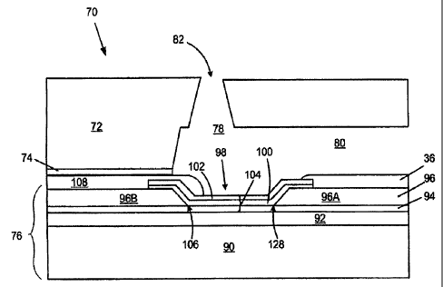
reference to FIGS. 6-9. FIG. 6 is a cross-sectional view, not to scale, of a
micro-fluid
ejection head 70 according to a first embodiment of the disclosure. In this
embodiment, the ejection head 70 includes a flow feature member 72 attached,
as by
an adhesive 74, adjacent (e.g., to) a semiconductor substrate 76. The flow
feature
member 72 has a thickness ranging from about 5 to 65 microns, and can be made
from a chemically resistant polymer such as polyimide. Flow features, such as
a fluid
chamber 78, fluid supply channel 80 and nozzle 82, can be formed in the flow
feature
, member 72 by conventional techniques, such as laser ablation. The
embodiments
described herein are not limited by the foregoing flow feature member 72. In
an
alternative embodiment, the flow feature member may comprise fluid chambers
and
the fluid supply channel in a thick film layer to which a nozzle plate is
attached, or the
CA 02631454 2008-05-28
WO 2007/076029 PCT/US2006/049063
9
flow features may be formed in both a thick film layer and a nozzle -plate.
FIG. 9,
described below, illustrates an embodiment of a micro-fluid ejection head 84
having a
thick film layer 86 and nozzle plate 88 attached to the thick film layer 86.
The semiconductor substrate 76 to which the flow feature member 72 is
attached includes a support substrate 90 made of an insulating or
semiconductive
material as described above with reference to FIG. 1. In the case of a
semiconductive
material for substrate 90, an insulating layer 92 similar to layer 16 is
applied to the
substrate 90. A resistive layer 94 similar to resistive layer 18, described
above, is
applied to the insulating layer 92. Likewise, a conductive layer 96 similar to
conductive layer 34 is applied to the resistive layer 94 and is etched to
provide the
power and ground conductors 96A and 96B for activating a micro-fluid ejection
actuator 98 defined between the conductors 96A and 96B.
An advantage of at least some of the disclosed embodiments is that a number
and thickness of protective layers for the micro-fluid ejection actuator 98
may be
reduced in order to reduce power consumption without adversely affecting the
life of
the micro-fluid ejection actuators 98.
Unlike the ejection head 10 illustrated in FIG. 1, the ejection head 70 has a
single protective layer 100 and, optionally, a relatively thin cavitation
layer 102. The
protective layer 100 may be provided by a material selected from the group
consisting
of diamond-like carbon (DLC), silicon doped diamond-like carbon (Si-DLC)
titanium, tantalum, silicon nitride and an oxidized metal. The thickness of
the
protective layer 100 may range from about 400 to about 3000 Angstroms. Such a
protective layer 72 thickness provides an ejection actuator stack 104 having a
thickness ranging from about 1200 to about 6500 Angstroms. When used, the
cavitation layer 102 may have a thickness ranging from about 500 to about 3000
Angstroms.
In order to, for example, reduce damage caused by thermal expansion and
cavitation adjacent a distal edge 106 of the micro-fluid ejection actuator 98,
a
polymeric layer 108 having a degradation temperature of less than about 400
C. is
applied to the protective layers 100 and 102 and conductive layer 96 so that
the
polymeric layer overlaps a portion of the micro-fluid ejection actuator 98 as
shown in
CA 02631454 2008-05-28
WO 2007/076029 PCT/US2006/049063
plan view in FIG. 7 adjacent the distal edge 106 thereof. Due to the
relatively low
degradation temperature of the polymeric layer 108, the overlapped portion of
the
actuator 98 should be less than about five microns. Typically, the overlapped
portion
of the actuator 98 will range from about one to about four microns.
5 A temperature profile for the micro-fluid ejection actuator 98 is shown by
Curve A in FIG. 8. As shown in FIG. 8, the micro-fluid ejection actuator 98
has a
temperature of about 400 C. in a central portion of the actuator whereas, the
edge
106 of the actuator has a temperature of about 150 C. At about five microns
from the
edge 106 of the actuator 98, point B on Curve A, the temperature is about 325
C.
10 which is the nucleation temperature indicated by dashed line 110 for
ejecting fluid
from the micro-fluid ejection head 70. Accordingly, if less than five microns
of the
actuator 98 adjacent edge 106 is overlapped with the polymeric layer 108, the
polymeric layer may be below its decomposition temperature.
A suitable polymeric layer 108 having a degradation temperature below about
400 C. is a cross-linked epoxy material such as described in U.S. Patent No.
6,830,646 to Patil et al., the disclosure of which is incorporated herein by
reference.
The polymeric layer 108, in the case of micro-fluid ejection head 70, may be
applied
as a planarization layer having a thickness averaging from about one to about
ten
microns. Spin coating, spraying, dipping, or roll coating processes may be
used to
apply the polymeric layer 108 to the conductive layer 96 and protective layers
100
and 102. It will be appreciated that the overlapped portion of the actuator 98
may
have a greater thickness of polymeric layer 108 so that a relatively smooth
planarization layer may be obtained.
With reference now to FIGS. 9 and 10, alternate embodiments of the
disclosure will now be described. As set forth above, the micro-fluid ejection
head 84
illustrated in FIGS. 9 and 10 includes a thick film layer 86 providing the
flow feature
member containing a fluid chamber 120 and fluid supply channel 122. The thick
film
layer 86 may also be made of a cross-linked epoxy material as set forth above.
However, the thick film layer 86 has a thickness ranging from about 4 to about
40
microns or more. As with the polymeric layer 108, the thick film layer
overlaps a
portion of the micro-fluid ejection actuator 98 as shown in FIGS. 9 and 10.
The
CA 02631454 2008-05-28
WO 2007/076029 PCT/US2006/049063
11
overlapped portion, adjacent the distal edge 106 may also be less than about
five
microns and may range from about one to about four microns.
The thick film layer 86 may be made of the same material as the polymeric
layer 108; in which case there may be no need for a separate polymeric layer
108
between the thick film layer 86 and the conductive layer 96 and protective
layers 100
and 102. The thick film layer 86 may be applied in the same manner as the
polymeric
layer 108 described above. Each of the polymeric layer 108 and thick film
layer 86
may be photoimaged and developed using conventional photoimaging and
developing
techniques to provide the less than five micron overlap of the actuator 98. In
the case
of the thick film layer 86, the photoimaging and developing techniques may
also be
used to provide the fluid chamber 120 and fluid supply channel 122 therein.
After imaging and developing the thick film layer 86, a nozzle plate 88 made
of a polyimide material or a pliotoresist material may be attached to the
thick film
layer 86. In the case of a polyimide nozzle plate 88, a nozzle 124 for each of
the
actuators may be laser ablated in the nozzle plate 88. If the nozzle plate 88
is made of
a photoresist material, photoimaging and developing techniques may be used to
make
the nozzle 124.
In another alternative embodiment, illustrated in FIGS. 9 and 10, a polymeric
layer 126 may overlap a proximal edge 128 of the actuator 98 so that both the
distal
edge 106 and the proximal edge 128 of the actuator 98 are overlapped less than
about
five microns, typically from about one to about four microns. The polymeric
layer
126, as illustrated in FIGS. 9 and 10, may likewise be applied to overlap the
proximal
edge 128 of the actuator illustrated in FIGS. 6 and 7. In the embodiment
illustrated in
FIGS. 9 and 10, the polymeric layer 126 may be the same as the thick film
layer 86
except that the thickness of the polymeric layer 126 will be reduced in the
fluid
supply channel 122 of the ejection head 84 by imaging and developing the
polymeric
layer 126.
The micro-fluid ejection head 70 or 84 may be permanently or removably
attached to a fluid supply cartridge 128 as shown in FIG. 11. As shown in FIG.
5, the
ejection head 70 or 84 may be attached to an ejection head portion 130 of the
fluid
cartridge 128. A main body 132 of the cartridge 128 includes a fluid reservoir
for
CA 02631454 2008-05-28
WO 2007/076029 PCT/US2006/049063
12
supply of fluid to the micro-fluid ejection head 70 or 84. A flexible circuit
or tape
automated bonding (TAB) circuit 134 containing electrical contacts 136 for
connection to an ejection head control device, such as an ink jet printer, is
attached to
the main body 132 of the cartridge 128. Electrical tracing 138 from the
electrical
contacts 136 are attached to the substrate 76 (FIGS. 6 and 9) to provide
activation of
micro-fluid ejection actuator 98 on demand from the control device to which
the fluid
cartridge 128 is attached. The disclosure, however, is not limited to the
fluid
cartridges 128 as illustrated in FIG. 11 as the micro-fluid ejection head 70
or 84
according to the disclosure may be used for a wide variety of fluid
cartridges, wherein
the ejection head 70 or 84 may be remote from the fluid reservoir of main body
128.
It is contemplated, and will be apparent to those skilled in the art from the
preceding description and the accompanying drawings, that modifications and
changes may be made in the embodiments of the disclosure. Accordingly, it is
expressly intended that the foregoing description and the accompanying
drawings are
illustrative of exemplary embodiments only, not limiting thereto, and that the
true
spirit and scope of the present disclosure be determined by reference to the
appended
claims.