Note: Descriptions are shown in the official language in which they were submitted.
CA 02631600 2011-09-22
1
METHOD FOR FORMING AN ELECTRONIC PAPER DISPLAY
TECHNICAL FIELD
[0001] Described are methods for forming an electronic paper display with
microcapsules having encapsulated reimageable media. The microcapsules may be
applied to or developed on a substrate via single component development, two
component development, ballistic marking, liquid xerography, ion-charging
development or the like. The microcapsules may be or may not be mixed with
optional carrier particles prior to being applied to or developed on the
substrate. The
microcapsules may be pressed to prevent gaps from forming or from being
present
between the microcapsules and/or the substrate. The microcapsules may form a
display layer of microcapsules on the substrate to produce an electrophoretic
display
or a display device. In the display device, an electrical field may be applied
to the
microcapsules via a conducting substrate and/or electrodes to display a set of
first
colored particles or a set of second colored particles of the encapsulated
reimageable
media within the microcapsules. In this manner, the encapsulated reimageable
media
may be used in forming images with the electronic paper display.
REFERENCES
[0002] U.S. Patent No. 7,123,238, illustrates an electrophoretic display
device that includes a spacer layer positioned between two conductive film
substrates.
[0003] U.S. Patent No. 6,577,433, illustrates an electrophoretic display
device comprising a multiplicity of individual reservoirs, each containing an
electrophoretic display fluid, located between two conductive film substrates,
at least
one of which is transparent. The electrophoretic display fluid has at least
two sets of
particles dispersed in a transparent liquid system and one or more charge
directors
dissolved or dispersed in the liquid system or physically embedded on the
surface of
the particles or chemically bonded on the surface of the surface of the
particles. The
at least two sets of particles exhibit different, contrasting color and
different charging
properties from each other.
[0004] U.S. Patent No. 7,675,502, illustrates a display region between
substrates, at least one of which is transparent. The display region including
a
multiplicity of pixels, wherein
CA 02631600 2008-05-20
2
one or more of the pixels comprise three or more subpixels. The three or more
subpixels is comprised of individual reservoirs that each contains a display
medium
comprised of one or more set of colored particles in a dielectric fluid. The
display
medium includes two different colors therein so that the subpixel is capable
of
exhibiting each of the two different colors, and wherein each of the three or
more
subpixels include a display medium having a different combination of two
colors from
the display mediums of all of the other of the three or more subpixels.
BACKGROUND
100051 An electronic paper display may be formed by connecting a thin layer
of transparent plastic small beads, which are randomly dispersed, to a surface
of a
sheet. The beads have two hemispheres that have two contrasting colors, such
as
black and white, red and white or the like. The hemispheres are electrically
charged to
exhibit an electrical dipole. For example, the color red on a first hemisphere
may be
associated with a negative charge and the color white on a second hemisphere
may be
associated with a positive charge. The hemispheres of the beads are contained
within
an oil-filled cavity, and rotate within the oil-filled cavities based on
electrical charges
that attract or repel the electrically charged hemispheres. Thus, the sheet
receiving the
beads and/or the oil-filled cavities may be required to be stiff and rigid to
prevent
puncturing of the cavities or damaging of the cavities or the hemispheres of
the beads
by, for example crushing, flattening or the like.
100061 A voltage is applied to the surface of the sheet via one or more
electrode plates associated with the sheet. The voltage applied by the
electrode plates
provides an electric field which may attract one of the hemispheres of one or
more of
the beads based on the charge associated with that hemisphere. As a result,
one or
more of the beads are rotated by the attractive forces between one of the
hemispheres
of the beads, the charge associated with the hemispheres of the beads, and the
electric
field created by the electrode plates. As a result, the hemispheres of the
beads may
rotate to present one of the hemispheres in a viewing direction on the
electronic paper.
By rotating one or more beads to present one of the hemispheres for each bead,
the
hemispheres may form or may display an image on the electronic paper. As a
result,
the electric field applied to the surface of the sheet by the electrode plates
creates the
image that is viewable from a viewing direction of the electronic paper.
CA 02631600 2008-05-20
3
100071 However, connecting a thin layer of the beads having the oil-filled
cavities to the surface of the sheet to form the electronic paper is often
time
consuming and costly. Additionally, a resolution of the images formed on the
surface
of the electronic paper by the one or more beads tends to be lower because a
pixel
count per square inch for the thin layer of beads formed on the surface of the
sheet is
often minimal as compared to a resolution of a conventional display, such as
an LCD.
Further, increasing the pixels per square inch by increasing a number of beads
per
square inch on the surface of the sheet is burdensome because difficulties
exist for
positioning the oil-filled cavities at specific locations corresponding to
specific pixels
or subpixels. Moreover, sealing an increased number of oil-filled cavities to
the
surface of the sheet to increase the pixels per square inch is inconvenient
for forming
electronic paper via the beads. The rotation of the beads to display different
hemispheres often tends to be too slow for some display purposes, such as
screens and
the like. As a result, forming electronic paper with the beads having oil-
filled cavity
has an increased probability for manufacturing problems and often elevates
production
costs for the electronic paper.
100081 A need, therefore, exists for a system and a method for forming
electronic paper displays with microcapsules having encapsulated reimageable
media
in a more efficient and reliable manner. Further, a need exists for a system
and a
method for forming electronic paper displays by printing or developing
microcapsules
with or without carrier particles onto a substrate to form a display device.
Moreover,
a need exists for a system and a method for forming electronic paper displays
which
may position a substrate having microcapsules printed thereon adjacent to one
or more
conductive substrates for applying an electric field to the microcapsules.
SUMMARY
100091 Described herein is a method for forming an electronic paper display
with microcapsules having encapsulated reimageable media.
100101 Each microcapsule may have encapsulated reimageable media, such
as, for example, two differently colored particles suspended in a medium, and
may be
applied to a substrate in forming the electronic paper display. The
microcapsules may
be dried to form a dry powder of microcapsules for applying to the substrate.
Optional carrier particles may or may not be added to the dry powder for
developing
the dry powder on the substrate by two component development (with carrier) or
CA 02631600 2008-05-20
4
single component development (without carrier), respectively. Alternatively,
the
microcapsules may be included in an aerosol and/or liquid for applying the
microcapsules onto the substrate, for example by ballistic aerosol marking. In
another
alternative, the microcapsules may be suspended in a liquid carrier for
developing the
microcapsules on the substrate via liquid xerography. In yet another
alternative, the
microcapsules may be generated in an airborne stream to be ion-charged and
developed on the substrate by ion-charging development.
[0011] After applying or developing the microcapsules on the substrate, the
microcapsules may form a display layer of microcapsules on the substrate. The
resolution, that is, the density of the microcapsules applied onto the
substrate, may be
based on carrier particles and/or a size of the microcapsules. A protective
layer may
be applied to the microcapsules to provide mechanical protection for the
microcapsules. The substrate having the microcapsules may be positioned
between
conductive substrates for applying an electric field to the encapsulated
reimageable
media to display one or more images.
100121 According to aspects illustrated herein, there is provided a method
for forming a multi-color electrophoretic display. The method includes
providing
microcapsules, wherein the microcapsules have an electrostatic charge, and
wherein
the microcapsules comprise a shell that is transparent and a display medium
within the
shell, wherein the display medium is comprised of either (a) at least two sets
of
differently colored particles in a substantially clear fluid, or (b) at least
one set of
colored particles in a differently colored fluid. Further, the method includes
transferring the microcapsules to a substrate, wherein the electrostatic
charge of the
microcapsules attracts the microcapsules to the substrate, wherein a display
layer of
microcapsules is formed on the substrate. Moreover, the method includes
positioning
a conductive substrate adjacent to the substrate, wherein the substrate is
located
between the display layer and the conductive substrate. In use, the conductive
substrate applies an electric field to the display layer, and the sets of
particles within
each microcapsule in the display layer are movable within the microcapsule by
the
electric field.
100131 In embodiments, provided is a method for forming a multi-color
electrophoretic display. The method includes providing microcapsules, wherein
the
microcapsules comprise a shell that is transparent and a display medium within
the
CA 02631600 2008-05-20
shell, wherein the display medium is comprised of either (a) at least two sets
of
differently colored particles in a substantially clear fluid, or (b) at least
one set of
colored particles in a differently colored fluid. Further, the method includes
transferring the microcapsules to a substrate, wherein the microcapsules on
the
substrate define a display layer of microcapsules on the substrate. Moreover,
the
methods include positioning a conductive substrate adjacent to the substrate,
wherein
the substrate is located between the display layer and the conductive
substrate. In use,
the conductive substrate applies an electric field to the display layer, and
the sets of
particles of each microcapsule in the display layer are movable within the
microcapsule by the electric field.
100141 In other embodiments, provided is a method for forming a multi-
color electrophoretic display. The method includes electrostatically charging
microcapsules to form charged particles, wherein each microcapsule comprises a
shell
that is transparent, wherein a surface of the shell contains a charge control
agent or a
flow aid agent and a display medium within the shell, wherein the display
medium is
comprised of either (a) at least two sets of differently colored particles in
a
substantially clear fluid, or (b) at least one set of colored particles in a
differently
colored fluid. Further, the method includes transferring the charged particles
of
microcapsules to a substrate, wherein the microcapsules on the substrate
define a
display layer of microcapsules on the substrate. Moreover, the method includes
positioning a conductive substrate adjacent to the substrate, wherein the
substrate is
located between the display layer and the conductive substrate. In use, the
conductive
substrate applies an electric field to the display layer, and the sets of
particles of each
microcapsule in the display layer are movable within the microcapsule by the
electric
field.
100151 It is an advantage of the various embodiments described herein to
provide a method for forming an electronic paper display which may apply
microcapsules having two differently colored particles suspended in a display
medium
therein via ballistic aerosol marking, liquid xerography, ion-charging
development or
xerographical printing process, such as single component development, two
component development or the like. Another advantage of the various
embodiments
is to provide a method for forming an electronic paper display which may
dispense
microcapsules having encapsulated reimageable media onto a substrate to form a
high
resolution colored display. Moreover, another advantage of the various
embodiments
CA 02631600 2011-09-22
6
is to provide a method for forming an electronic paper display which may be
manufactured at a lower cost than a conventional display, such as a liquid
crystal
display or the like.
[015a] According to an aspect of the present invention, there is provided
a method for forming a multi-color electrophoretic display, the method
comprising:
providing microcapsules, wherein the microcapsules have an electrostatic
charge, and wherein the microcapsules comprise:
a shell that is transparent; and
a display medium within the shell, wherein the display medium is comprised
of either (a) at least two sets of differently colored particles in a
substantially clear
fluid, or (b) at least one set of colored particles in a differently colored
fluid;
transferring the microcapsules to a substrate, wherein the electrostatic
charge
of the microcapsules attracts the microcapsules to the substrate, wherein a
display
layer of microcapsules is formed on the substrate;
positioning a conductive substrate adjacent to the substrate, wherein the
substrate is located between the display layer and the conductive substrate,
wherein
the conductive substrate applies an electric field to the display layer, and
wherein the
sets of particles of each microcapsule in the display layer are movable within
the
microcapsule by the electric field; and
softening the microcapsules of the display layer after being transferred to
the
substrate, wherein gaps between the microcapsules or the microcapsules and the
substrate are reduced, and/or applying pressure to the microcapsules of the
display
layer after being transferred to the substrate, wherein gaps between the
microcapsules
or the microcapsules and the substrate are reduced.
1015b1 According to another aspect of the present invention, there is
provided a method for forming a multi-color electrophoretic display, the
method
comprising:
providing microcapsules, wherein the microcapsules comprise:
a shell that is transparent; and
a display medium within the shell, wherein the display medium is comprised
of either (a) at least two sets of differently colored particles in a
substantially clear
fluid, or (b) at least one set of colored particles in a differently colored
fluid;
transferring the microcapsules to a substrate, wherein the microcapsules on
the
substrate define a display layer of microcapsules on the substrate;
CA 02631600 2011-09-22
6a
positioning a conductive substrate adjacent to the substrate, wherein the
substrate is located between the display layer and the conductive substrate,
wherein
the conductive substrate applies an electric field to the display layer,
wherein the sets
of particles of each microcapsule in the display layer are movable within the
microcapsule by the electric field; and
softening the microcapsules of the display layer after being transferred to
the
substrate, wherein gaps between the microcapsules or the microcapsules and the
substrate are reduced, and/or applying pressure to the microcapsules of the
display
layer after being transferred to the substrate, wherein gaps between the
microcapsules
or the microcapsules and the substrate are reduced.
[015c1 According to yet another aspect of the present invention, there is
provided a method for forming a multi-color electrophoretic display, the
method
comprising:
electrostatically charging microcapsules to form charged particles, wherein
each microcapsule comprises:
a shell that is transparent, wherein a surface of the shell contains a charge
control agent or a flow aid agent;
a display medium within the shell, wherein the display medium is comprised
of either (a) at least two sets of differently colored particles in a
substantially clear
fluid, or (b) at least one set of colored particles in a differently colored
fluid;
transferring the charged particles of microcapsules to a substrate, wherein
the
microcapsules on the substrate define a display layer of microcapsules on the
substrate;
positioning a conductive substrate adjacent to the substrate, wherein the
substrate is located between the display layer and the conductive substrate,
wherein
the conductive substrate applies an electric field to the display layer, and
wherein the
sets of particles of each microcapsule in the display layer are movable within
the
microcapsule by the electric field; and
softening the microcapsules of the display layer after being transferred to
the
substrate, wherein gaps between the microcapsules or the microcapsules and the
substrate are reduced, and/or applying pressure to the microcapsules of the
display
layer after being transferred to the substrate, wherein gaps between the
microcapsules
or the microcapsules and the substrate are reduced.
CA 02631600 2011-09-22
6b
[0016] Additional features and advantages of the various embodiments are
described herein and/or will be apparent from the description.
BRIEF DESCRIPTION OF THE DRAWINGS
[0017] FIG. 1 is a cross-sectional view of a microcapsule having suspended
sets of particles in a first state in an embodiment of the present disclosure.
[000518] FIG. 2 is a cross-sectional view of a microcapsule having suspended
sets of particles in a second state in an embodiment of the present
disclosure.
[0019] FIGS. 3-6 are steps for forming an electrophoretic display in an
embodiment of the present disclosure.
[000620] FIGS. 7 and 8 are top planar views of a layout having microcapsules
on a substrate in an embodiment of the present disclosure.
[0021] FIG. 9 is a flow chart of a method for forming an electrophoretic
display in an embodiment of the present disclosure.
EMBODIMENTS
[000722] Generally, in various exemplary embodiments, there is provided a
method for producing an electronic paper display with microcapsules having
encapsulated reimageable media suspended in a display medium. The encapsulated
reimageable media may include, for example, at least two differently colored
particle
sets suspended in the display media, the differently colored particles being
movable
within the display medium by an electric field. The microcapsules may be
applied to
or developed on the substrate by ballistic aerosol marking, single component
development or ion-charging development. In embodiments, a dry powder of
microcapsules may be mixed with optional carrier particles or a carrier liquid
prior to
application to the substrate by two component development or liquid
xerography,
respectively.
[0023] After application or development of the microcapsules on the
substrate, the microcapsules may form a display layer on the substrate. A
resolution
of the display layer of microcapsules, that is, the density of the
microcapsules
dispensed onto the substrate, may be based on or associated with a size of the
microcapsules and/or a size of the carrier particles applied to the substrate.
A coating
CA 02631600 2008-05-20
7
may be applied to the display layer to protect the microcapsules and the
substrate from
damaging mechanical forces. The substrate and the microcapsules may be
positioned
between conductive substrates to form an electrophoretic display or a display
device.
The conductive substrates may be used to apply an electric field to the
encapsulated
reimageable media of the microcapsules to manipulate movement of the particles
so
that specific colors are seen by a viewer at locations and/or pixels, thereby
displaying
an image with the encapsulated reimageable media of the microcapsules.
[0024] A color display refers to, for example, any display capable of
displaying at least two different colors. Examples include black and white
colors, as
well as full color displays such as red, green, blue and/or black, or cyan,
magenta,
yellow and/or black, and highlight color displays, including two colors
highlighted
and/or shaded with a third color.
[0025] In embodiments, the microcapsules encapsulate reimageable media
(electrophoretic display medium) comprised of at least one fluid and at least
one, for
example at least two, such as from two to ten or from two to four, set(s) of
colored
particles dispersed in the fluid.
[0026] The encapsulated reimageable media comprises one or more sets of
colored particles dispersed in a display medium or a fluid system. The display
medium or the fluid may be either clear/transparent, or it may exhibit a
visible color,
for example a different, contrasting color from the color(s) exhibited by the
sets of
particles dispersed therein. A colored fluid is typically used in a display
employing a
single set of colored particles, for example white particles, with the color
of the fluid
being a contrasting color other than white.
[0027] In embodiments, the fluid of the microcapsules and the set(s) of
particles therein may have densities that are substantially matched, for
example
wherein the densities of these materials are within about 25% of each other,
or more
specifically within 20% of each other or within 10% of each other. The density
of the
colored particles and/or the electrophoretic particles for the encapsulated
reimageable
media may be substantially matched to that of the suspending fluid. For
example, a
suspending fluid may have a density that is "substantially matched" to the
density of
the colored particles and/or the electrophoretic particles dispersed therein
if the
difference in their respective densities is from about zero to about 2 giml,
for example
from about zero to about 0.5 g/ml.
CA 02631600 2008-05-20
8
[0028] The fluid may comprise from about 10% to about 95% by weight of
the encapsulated reimageable media, for example from about 30% to about 90% or
from about 40% to about 80% by weight of the display medium.
[0029] The fluid may be comprised of any suitable fluid known in the art for
use in electrophoretic displays. Fluid refers to, for example, a material in a
liquid
state, and is not a gas or air. Of course, air or any other gas may also be
present in the
microcapsules of the display device, but the fluid of the microcapsules refers
to a fluid
in a liquid state. The choice of fluid may be based on concerns of chemical
inertness,
density matching to the particles to be suspended therein and/or chemical
compatibility with the particles. In embodiments, the suspending fluid may
have a
low dielectric constant (for example, about 4 or less, such as about 0.5 to
about 2).
The viscosity of the fluid may be relatively low at the temperatures of
operation in
order to permit the particles to move therein, for example under the influence
of an
electrical field. In embodiments, the fluid may have a kinematic viscosity in
the range
of about 0.25 centistokes to about 10 centistokes, for example from about 0.5
centistokes to about 5 centistokes or from about 1 centistoke to about 2
centistokes, at
about room temperature (about 23 C to about 27 C). The fluid may be dielectric
and
substantially free of ions. The fluid also may have minimum solvent action on
the
colored particles therein, and a specific gravity substantially equal to the
colored
particles, for example within about 20% of each other. Additionally, the fluid
may be
chosen to be a poor solvent for some polymers, which is advantageous for use
in the
fabrication of particles because it increases the range of polymeric materials
useful in
fabricating particles.
[0030] In embodiments, organic solvents such as halogenated organic
solvents, saturated linear or branched hydrocarbons, silicone oils, and low
molecular
weight halogen-containing polymers are a few suitable types of fluids that may
be
used. Organic solvents may include, for example, epoxides such as, for
example,
decane epoxide and dodecane epoxide, vinyl ethers such as, for example,
cyclohexyl
vinyl ether, and aromatic hydrocarbons such as, for example, toluene and
naphthalene.
Halogenated organic solvents may include, for example,
tetrafluorodibromoethylene,
tetrachloroethylene, trifluorochloroethylene, 1,2,4-trichlorobenzene, carbon
tetrachloride, mixtures thereof and the like. These materials may have high
densities.
Hydrocarbons may include, for example, decane, dodecane, tetradecane, xylene,
CA 02631600 2008-05-20
9
toluene, hexane, cyclohexane, benzene, the aliphatic hydrocarbons in the
ISOPARTM
(Exxon), NORPARTM (a series of normal paraffinic liquids from Exxon), SHELL-
SOLTM (Shell), and SOL-TROLTm (Shell) series, naphtha, and other petroleum
solvents. These materials may have low densities. Examples of silicone oils
include
octamethyl cyclosiloxane and higher molecular weight cyclic siloxanes,
poly(methyl
phenyl siloxane), hexamethyldisiloxane and polydimethylsiloxane. These
materials
may have low densities. Low molecular weight halogen-containing polymers may
include, for example, poly(chlorotrifluoroethylene) polymer or KRYTOXTm
polymers (Dupont).
[0031] Typically, hydrocarbon fluids such as 1SOPAR M are used for =
electrophoretic ink applications due to their low cost, good dielectric
strength, low
volatility, and nonreactivity. Further, mixtures of above mentioned fluids are
sometimes advantageous. For examples, it would be desirable to adjust or
change the
viscosity, density, and other physical properties of the fluid by mixing
different fluids.
100321 In embodiments, the aliphatic hydrocarbons may cause degradation
of performance, for example when non-crosslinked emulsion aggregation
particles are
used as the colored particles of the encapsulated reimageable media and/or
when the
colored particles are imparted with a charge by treatment with a surface
coating that
can be desorbed from the particle surface in the presence of an aliphatic
hydrocarbon.
Thus, it may be desirable to use, as the fluid of the encapsulated reimageable
media, a
nonswelling fluid such as a silicone fluid. A commercially available silicone
fluid
includes DOW 200, a polydimethylsiloxane polymer available from Dow Corning.
Other examples of suitable silicone fluids include polydimethylsiloxane fluids
available from Gelest Corporation such as trimethylsiloxy terminated fluids
DMS-
TOO, DMS-T01, DMS-T01.5, DMS-T02, DMS-T03, DMS-T05, DMS-T07, DMS-
T11; cyclomethicones such as SI06700.0, S1D2650.0, SID4625.0 (also known as
D4,
D5, and D6 fluids, respectively); phenylmethylsiloxanes such as PMM-0011, PDM-
7040; fluorosilicones such as SIB1816.0; polydiethylsiloxanes such as DES-T03,
DES-T11; branched and low viscosity phenyltris(trimethylsiloxy)silane fluids
such as
S1P6827.0, phenethyltris(trimethylsiloxy)silane fluids such as S1P6722.8, and
the like.
[0033] If colored, the fluid may be colored by any suitable means in the art,
including through the inclusion of suitable dispersible colorants such as dyes
and/or
dispersible pigments therein.
CA 02631600 2008-05-20
100341 In embodiments, the fluid is substantially free of charge control
additives and other ionic species that may affect the charging behavior of the
encapsulated reimageable media and/or the particles dispersed therein.
However, in
other embodiments, the fluid may contain additives such as surface modifiers
to
modify the surface energy or charge of the particles and such as charge
control agents,
dispersants, and/or surfactants.
[0035] In embodiments, the encapsulated reimageable media includes at
least one set of particles exhibiting substantially the same color. The
encapsulated
reimageable media may be comprised of one set of colored particles, including
at least
two, such as from two to ten or from two to four, sets of differently colored
particles
dispersed in the fluid. Color refers to, for example, the overall absorption
characteristic within the range of wavelengths of the electromagnetic
spectrum.
Substantially the same color herein refers to, for example, particles
exhibiting
substantially the same hue and contrast (darkness/lightness) as other
particles in the
set. Colored particles of different sets of particles in the encapsulated
reimageable
media exhibit a color, that is, an absorption characteristic, different from
each other.
For example, if a first set of particles exhibits a yellow color, then a
second differently
colored set of particles will exhibit a different shade (hue and/or contrast)
of yellow or
a different color altogether, for example such as cyan or magenta.
[0036] An encapsulated reimageable media may include two sets of
differently colored particles, for example black particles and white
particles. In
embodiments, the encapsulated reimageable media comprises at least three
differently
colored sets of particles. As examples, the three sets of colored particles
may
comprise the three subtractive primary colors yellow, cyan and magenta, or may
comprise red, blue and green. An example encapsulated reimageable media
containing four sets of differently colored particles may comprise yellow,
cyan,
magenta and black. Additional differently colored sets of particles, for
example for
highlight coloring, may be included as additional sets of colored particles in
any
embodiment described herein.
[0037] In embodiments, it is desirable to have several different two particle
microcapsules comprise a portion of the display equivalent to one pixel of the
display.
Each microcapsule in the pixel may include a set of white particles and a set
on non-
white particles, or different colors of two different non-white colors. For
example,
CA 02631600 2008-05-20
11
different microcapsules of a same pixel may comprise red/white, blue/white,
green/white and optionally black/white, or red/green, blue/green, red/blue and
optionally black/white, color combinations.
[0038] Each particle within a first set of particles may display, may present
or may provide a first color. Further, each particle within a second set of
particles
may display, may present or may provide a second color different from the
first color.
In embodiments, a first set of particles may be a color, such as red, orange,
yellow,
green, blue, green or black, and a second set of particles may be white.
Alternatively,
the first set of particles may be a color and the second set of particles may
be a
different non-white color. In embodiments, the first set of particles may be
one of
cyan, yellow, magenta and black. Moreover, the second set of particles may be
a
different one of cyan, yellow, magenta and black than the first set of
particles.
[0039] In embodiments, a third set of particles and/or a fourth set of
particles may be optionally included with the first set of particles and
second set of
particles within the shell or suspended in the display medium of the
microcapsules.
For example, a first set of particles may be cyan, a second set of particles
may be
yellow, a third set of particles may be magenta and a fourth set of particles
may be
black. In embodiments, the third set of particles and/or the fourth set of
particles may
be colored particles or electrophoretic particles. The present disclosure
should not be
deemed as limited to specific embodiments of the sets of particles. It should
be
understood that the number of particles sets within the shell of the
microcapsule may
be any number of particles sets as known to one of skill in the art.
[0040] Each set of same colored particles in the microcapsules may
comprise from about 5% to about 50% by weight, for example from about 5% to
about 40% or from about 5% to about 30% by weight, of the microcapsules.
[0041] In embodiments, described is a low electrical conductivity
electrophoretic encapsulated reimageable media, for example having a
conductivity on
the order of about 10-11 to about 10-15 S/m, such as from about 10-12 to about
10-14 S/m
or from about 10-12 to about 10-13 S/m. The conductivity of the encapsulated
reimageable media is thus comparable to that of the dielectric fluid. The
particles of
the encapsulated reimageable media may become charged by the application of a
high
electric field thereto, which may also be referred to as field-induced or in
situ
charging, in which particle charging is dependent on, for example, the field
strength
CA 02631600 2008-05-20
12
and the charging time (or number of charging cycles). Following charging, the
particles may have a charge (charge to mass ratio) on the order of
microcoulombs
( C) per gram (that is, on the order of 10-6 C/g), such as from about 0.1 to
about 20
C/g, from about 0.2 to about 10 [1.C/g or from about 0.3 to about 5 iC/g.
100421 The microcapsules, including the fluid and particle sets therein, of
embodiments herein may thus be made to be substantially free of charge control
additives and similar excess ionic species affecting the charging
characteristics and/or
conductivity of the encapsulated reimageable media. Substantially free of ions
herein
refers, for example, to the encapsulated reimageable media being free of ionic
species
to the extent that the aforementioned conductivity values may be achieved. As
a
result, the encapsulated reimageable media herein is able to exhibit the
aforementioned low conductivity properties.
100431 As a result of the desired absence of charge control additives in the
=microcapsules, the particles of the sets of particles of the encapsulated
reimageable
media need to be made to include a capability of exhibiting the low charging
property
by other methods. Such may be accomplished, for example, by the formation of
the
particles in the presence of a surfactant and/or water, wherein small amounts
of these
materials may be incorporated into the particles during formation. Other
components
that could impart the charge to the particles include polymerization
initiators such as
APS (ammonium persulfate), chain transfer agents such as DDT (dodecylthiol),
or
acidic/basic functional groups in the polymer backbone that may be exposed or
partially exposed on the particle surface. These materials may act as charge
species in
the particles, imparting an almost negligible charge at time zero but that
which
enables the particles to be charged, for example through application of a high
electric
field as will be described more fully below, to the low charge values
described above.
These materials are part of the particles and substantially do not become
dissociated in
the encapsulated reimageable media, thereby enabling the encapsulated
reimageable
media to maintain the low conductivity. Moreover, unlike prior systems
requiring the
= presence of ionic species in the encapsulated reimageable media that
permit the
display to degrade in performance over time, for example through the
generation of
wrong sign particles and/or loss of sufficient ionic species in the medium,
the particles
herein do not generate ionic species and do not require the presence of ionic
species
for charging, and thus are not subject to such degradation risks.
CA 02631600 2008-05-20
13
[0044] As the particles of the encapsulated reimageable media, any particle
made by any suitable process may be used, so long as the particles are capable
of
exhibiting the low charge property discussed above. Thus, particles made by
both
physical grinding methods, in which the material of the particles is formed as
a mass
that is then crushed and ground to the desired average particle size, and
chemical
build-up methods, in which the particles are grown individually within a
reaction
medium to the desired average particle size, both of which types of methods
are well
known in the toner art, may be used. The particles may be made to have an
average
size of from, for example, about 5 nm to about 100 p.m, such as from about 10
nrn to
about 50 p.m or from about 0.5 pm to about 25 11M. The particles have a size
less than
the size of the shells of the microcapsules in which the display medium will
be
contained so that the particles are free to move within the shells.
[0045] The particles may be neat pigments, dyed (laked) pignents,
pigment/polymer composites, dyed or pigmented agglomerated polymer particles
and
the like. As the colorant of the particles, dyes, pigment, mixtures of dyes,
mixtures of
pigments or mixtures of dyes and pigments may be used. Particles and/or
colorant of
particles may also include laked, or dyed, pigments, in which a dye is
precipitated on
the particles or the particles are stained with a dye such as metal salts of
readily
soluble anionic dyes, for example dyes of azo, triphenylmethane or
anthraquinone
structure containing one or more sulphonic or carboxylic acid groupings
precipitated
by a calcium, barium or aluminum salt.
100461 Typical manufacturing techniques for the above particles are drawn
from the liquid toner and other arts and include ball milling, attrition, jet
milling, and
the like. A pigmented polymer particle may be made by, for example,
compounding a
pigment in the polymer. The composite material is then (wet or dry) ground to
a
desired size. It may then optionally be added to a carrier liquid and milled
under high
shear for several hours to a final particle size and/or size distribution.
[0047] Chemical processes that may be used in forming the particles
include, for example, emulsion aggregation, dispersion polymerization, mini-
or
micro-emulsion polymerization, suspension polymerization, precipitation, phase
separation, solvent evaporation, in situ polymerization, or any process of
microencapsulation.
CA 02631600 2008-05-20
14
[0048] Polymers that may be used for the pigmented particles include, for
example, polystyrene, polyethylene, polypropylene, phenolic resins, ethylene-
vinyl
acetate copolymers, polyesters, polyacrylates, polymethacrylates, ethylene
acrylic acid
or methacrylic acid copolymers, acrylic copolymers and terpolymers and the
like.
Specific example include, for example, polyethylene, polypropylene,
polymethylmethacrylate, polyisobutylmethacrylate, polystyrene, polybutadiene,
polyisoprene, polyisobutylene, polylauryl methacrylate, polystearyl
methacrylate,
polyisobornyl me.thacrylate, poly-t-butyhmethacrylate, polyethyl methacrylate,
polymethyl acrylate, polyethyl acrylate, polyacrylonitrile, and copolymers of
two or
more of these materials.
[0049] In embodiments, the particles for the encapsulated reimageable
media are emulsion aggregation particles, for example including polyester
resin based
emulsion aggregation particles and styrene-acrylate or acrylate resin based
emulsion
aggregation particles. Such particles are chemically grown and tend to be
substantially monodisperse in size and substantially spherical in shape.
Another
advantage to emulsion aggregation particles is that the particle surface is
substantially
completely passivated by the binder resin, which may eliminate the
contribution of the
colorant, such as pigment, to the particle charge.
[0050] As surfactants for use in making emulsion aggregation particles as
discussed above, examples include anionic, cationic, nonionic surfactants and
the like.
[0051] The particle preparation is typically carried out in an aqueous (water)
environment as detailed above, and the electrophoretic encapsulated
reimageable
media is an non-aqueous environment (oil). When the particles are prepared,
they are
given a final water wash to remove excess surfactant. Trace amounts of
residual
surfactant on the surface of the particles, or trapped within the particles,
may remain
and contribute to the low conductivity of the particles. However, the amount
of
surfactant that actually gets into the oil is very low, since it prefers to be
in water. As
a result, the fluid medium has a desired low conductivity.
100521 In embodiments, the emulsion aggregation particles are made to have
an average particle size of from about 0.5 to about 25 pm, for example about 5
to
about 15 pm or about 5 to about 12 m. The particle size may be determined
using
any suitable device, for example a conventional Coulter counter.
CA 02631600 2011-09-22
. .
[0053] Although not required, the toner may also include additional known
positive or negative charge additives in effective suitable amounts of, for
example,
from about 0.1 to about 5 weight % of the toner, such as quaternary ammonium
compounds inclusive of alkyl pyridinium halides, bisulfates, organic sulfate
and
sulfonate compositions such as disclosed in U.S. Patent No. 4,338,390, cetyl
pyridinium tetrafluoroborates, distearyl dimethyl ammonium methyl sulfate,
aluminum salts or complexes, and the like.
[0054] Examples of pigments that may be used as the particles herein, or
that may be used as the colorant in polymer particles, include neat pigments
such as,
for example, titania, barium sulfate, kaolin, zinc oxide, carbon black and the
like. The
pigment should be insoluble in the suspending fluid. Additional pigments may
include, for example, carbon black such as REGAL 330 carbon black, acetylene
black, lamp black, aniline black, Violet PALIOGENTM Violet 5100 (BASFTm);
PALIOGEN Violet 5890 (BASF); HELIOGENTM Green L8730 (BASF); LITHOLTm
Scarlet D3700 (BASF); SUNFAST Blue 15:4 (Sun Chemical 249-0592);
Hostaperm Blue B2G-D (ClariantTm); Permanent Red P-F7RK; Hostaperm Violet BL
(Clariant); LITHOL Scarlet 4440 (BASF); Bon Red C (Dominion Color CompanyTm);
ORACETTm Pink RF (CibaTm); PALIOGEN Red 3871 K (BASF); SUNFAST Blue
15:3 (Sun Chemical 249-1284); PALIOGEN Red 3340 (BASF); SUNFAST
Carbazole Violet 23 (Sun Chemical 246-1670); LITHOL Fast Scarlet L4300 (BASF);
Sunbrite Yellow 17 (Sun Chemical 275-0023); HELIOGEN Blue L6900, L7020
(BASF); Sunbrite Yellow 74 (Sun Chemical 272-0558); SPECTRA PAC C Orange
16 (Sun Chemical 276-3016); HELIOGEN Blue K6902, K6910 (BASF);
SUNFAST Magenta 122 (Sun Chemical 228-0013); HELIOGEN Blue D6840,
D7080 (BASF); Sudan Blue OS (BASF); NEOPENTM Blue FF4012 (BASF); PV Fast
Blue B2G01 (Clariant); IRGAL1'IETM Blue BCA (Ciba); PALIOGEN Blue 6470
(BASF); Sudan Orange G (Aldrich), Sudan Orange 220 (BASF); PALIOGEN Orange
3040 (BASF); PALIOGEN Yellow 152, 1560 (BASF); LITHOL Fast Yellow 0991 K
(BASF); PALIOTOL Yellow 1840 (BASF); NOVOPERMTm Yellow FGL (Clariant);
Lumogen Yellow D0790 (BASF); Suco-Yellow L1250 (BASF); Suco-Yellow D1355
.
(BASF); Suco Fast Yellow Dl 355, Dl 351 (BASF); HOSTAPERMTm Pink E 02
(Clariant); Hansa Brilliant Yellow 5GX03 (Clariant); Permanent Yellow GRL 02
(Clariant); Permanent Rubine L6B 05 (Clariant); FANALTM Pink D4830 (BASF);
CINQUASIATM Magenta (DU PONTTm),
CA 02631600 2008-05-20
16
PALIOGEN Black L0084 (BASF); Pigment Black K801 (BASF); mixtures thereof
and the like.
100551 In polymer particles, the colorant may be included in the particles in
an amount of from, for example, about 0.1 to about 75% by weight of the
particle, for
example from about 1 to about 50% by weight or from about 3 to about 25% by
weight of the particle.
[00561 In any of the foregoing particle embodiments, the particles may also
include one or more external additives on the surfaces thereof. Such external
additives may be applied by blending, for example with a Henschel blender. In
embodiments, the external additive package may include one or more of silicon
dioxide or silica (Si02), titanium dioxide or titania (Ti02), titanic acid,
cerium oxide,
calcium or zinc stearate, and the like. The particles may have an average size
(diameter) of from about 5 nm to about 250 nm. Mixtures of differently sized
particles may also be used, for example a first silica having an average
primary
particle size, measured in diameter, in the range of, for example, from about
5 nm to
about 50 nm, such as from about 5 nm to about 25 nm or from about 20 nm to
about
40 nm and a second silica having an average primary particle size, measured in
diameter, in the range of, for example, from about 100 nm to about 200 nm,
such as
from about 100 nm to about 150 nm or from about 125 nm to about 145 nm. The
external additive particles may also be treated with a surface material.
100571 In embodiments, the external additives may be used to impart charge
to the particles. For example, a silica particle treated with
polydimethylsiloxane
(PDMS) or hexamethyldisilane (HMDS) can impart a positive charge. A titanic
acid
treated with isobutyl trimethoxysilane can impart a negative charge.
10058] In embodiments, the microcapsules may be made to have a size
(diameter) of from, for example, about 5 microns to about 1,000 microns, such
as
from about 5 to about 200 microns or from about 5 to about 50 microns.
(0059] For making the microcapsules, any suitable method of encapsulation
may be used. The process of encapsulation may include conventional or complex
coacervation, interfacial polymerization, in-situ polymerization, electrolytic
dispersion
and cooling, or spray-drying processes. In these processes, the display medium
is
added to a solution of the wall-forming material to be encapsulated thereby,
and the
= resulting encapsulated microspheres may be subjected to crosslinking. The
CA 02631600 2011-09-22
17
microcapsules may be prepared using melamine-formaldehyde, urea-formaldehyde,
resorcinol-formaldehyde, phenol-formaldehyde, gelatin-formaldehyde, isocyanate-
polyol, interpolymer complexes of two oppositely charged polymers such as
gelatin/gum arabic, gelatin/polyphosphate, and poly(styrene sulfonic
acid)/gelatin,
hydroxypropyl cellulose, mixtures and/or combinations of the foregoing, and
the like,
as microcapsule wall-forming materials.
[0060] The interfacial polymerization approach may rely on the presence of
an oil-soluble monomer in an electrophoretic composition, which is present as
an
emulsion in an aqueous phase. The monomers in the minute hydrophobic droplets
may react with a monomer to be introduced into the aqueous phase, polymerizing
at
the interface between the droplets and the surrounding aqueous display medium
and
forming shells around the droplets. Although the resulting walls are
relatively thin
and may be permeable, this process does not require the elevated temperatures
characteristic of some other processes, and therefore affords greater
flexibility in
terms of choosing the display medium.
[00081] Coating aids may be used to improve the uniformity and quality of
printed or developed electrophoretic microcapsules. Wetting agents are
typically
added to adjust the interfacial tension at the microcapsule/substrate
interface and to
adjust the liquid/air surface tension. Wetting agents include, for example,
anionic and
cationic surfactants, and nonionic species, such as silicone or fluoropolymer-
based
materials. Dispersing agents may be used to modify the interfacial tension
between
the microcapsules and binder or the substrate, providing control over
flocculation and
particle settling.
[0062] Surface tension modifiers may be added to adjust the air/ink
interfacial tension. Polysiloxanes are typically used in such an application
to improve
surface leveling while minimizing other defects within the coating. Surface
tension
modifiers include, for example, fluorinated surfactants, such as, for example,
the
ZONYLTM series from DuPont, the FLUORADTM series from 3MTm (St. Paul, Minn.),
and the fluoroalkyl series from Autochem; siloxanes, such as, for example,
SILWETTm from Union CarbideTM; and polyethoxy and polypropoxy alcohols.
Antifoams, such as silicone and silicone-free polymeric materials, may be
added to
enhance the movement of air from within a microcapsule formation solution to a
surface of the substrate and to facilitate the rupture of bubbles at the
surface. Other
useful antifoams
CA 02631600 2008-05-20
18
include, for example, glyceryl esters, polyhydric alcohols, compounded
antifoams,
such as oil solutions of alkylbenzenes, natural fats, fatty acids, and
metallic soaps, and
silicone antifoaming agents made from the combination of dimethyl siloxane
polymers and silica. Stabilizers such as UV-absorbers and antioxidants may
also be
added to improve the lifetime of the microcapsules.
100631 The coacervation approach may utilize an oil/water emulsion. One
or more colloids are coacervated (that is, agglomerated) out of the aqueous
phase and
deposited as shells around the oily droplets through control of temperature,
pH and/or
relative concentrations, thereby creating the microcapsule. Materials suitable
for
coacervation include gelatins and gum arabic.
100641 In an example complex coacervation process, the display medium to
be encapsulated is emulsified with the wall forming material, for example a
mixture of
water, gelatin and gum arabic, at an elevated temperature of, for example,
about 30 C
to about 80 C such as from about 35 C to about 75 C or from about 35 C to
about
65 C. The pH is then reduced, for example to less than 5, for example from
about 4
to about 5 such as from about 4.4 to about 4.9, through addition of an acid
such as
=
acetic acid and the like, to induce coacervation. The material of the wall of
the
microcapsules may then be crosslinked, for example by adding gluteraldehyde
and the
like and agitating the mixture in the presence of, for example, urea.
100651 The microcapsules may have a multi-layer wall around the particles
suspended within the display medium to define a shell of each microcapsule.
These
can be made, for example, by first forming a thin wall by an interfacial
polymerization
reaction, and subsequently forming a second, thicker wall by an in-situ
polymerization
reaction or by a coacervation process. The first wall of the microcapsule may
be
typically comprised of polyurea, polyurethane, polyamide, polyester, epoxy-
amine
condensates, silicones and the like. The second wall of the microcapsule may
be
comprised of condensates of melamine-formaldehyde, urea-formaldehyde,
resorcinol-
formaldehyde, phenol-formaldehyde, gelatin-formaldehyde, or interpolymer
complexes of two oppositely charged polymers such as gelatin/gum arabic and
poly(styrene sulfonic acid)/gelatin.
100661 A semi-continuous miniemulsion polymerization process may also
be used to encapsulate the electrophoretic display medium or the particles,
for
CA 02631600 2011-09-22
19
example as described in U.S. Patent No. 6,529,313.
[0067] A benefit of encapsulating the electrophoretic display medium is that
the microcapsules can be made to be spherical or other than spherical through
control
of the process. Different shapes may permit better packing density of the
microcapsules and better display quality.
[0068] Once generated, the microcapsules may then be applied to a substrate
by a known xerographical printing process, such as single component
development or
two component development. Alternatively, the microcapsules may be applied to
the
substrate by another known printing or application process, such as ballistic
aerosol
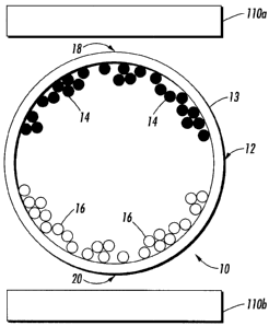
marking, liquid xerography, ion-charging development or the like.
[0069] In embodiments, the microcapsules may be mixed with or without
carrier particles and then printed on or developed on a substrate by, for
example,
known xerographical printing processes. The carrier particles may be
optionally
mixed with the microcapsules to form a two component developer. Without the
carrier particles, the microcapsules may be referred to a single component
developer.
The microcapsules may adhere to the surface of the substrate by, for example,
using
any suitable binder such as an adhesive or polymer matrix material that is
either
mixed with the microcapsules prior to developing the microcapsules on the
substrate,
coated onto the substrate before development of the microcapsules thereon,
coated
upon the microcapsules after developing on the substrate, or one or more of
the above,
including all three.
[0070] As an adhesive or binder, any material may be used, for example
including polyvinyl alcohol (PVA) or polyurethane such as NEOREZTM. A binder
may be used as an adhesive medium that supports and protects the
microcapsules, as
well as binds conductive substrate to the microcapsule dispersion. A binder
can be
non-conducting, semiconductive, or conductive. Binders are available in many
forms
and chemical types. Among these are water-soluble polymers, water-borne
polymers,
oil-soluble polymers, thermoset and thermoplastic polymers, and radiation-
cured
polymers.
[0071] Among water-soluble polymers are various polysaccharides,
polyvinyl alcohols, N-methylpyrrolidone, N-vinylpyrrolidone, various
CARBOWAXTM species (Union Carbide), and poly(2-hydroxyethyl acrylate).
CA 02631600 2011-09-22
[0072] The water-dispersed or water-borne systems are generally latex
compositions, for example NEOREZ and NEOCRYLTM resins (Zeneca ResinsTm),
ACRYSOLTM (Rohm and HaasTm), BAYHYDROLTM (BayerTm), and the HPTM
products (Cytec IndustriesTm). These may generally be lattices of
polyurethanes,
occasionally compounded with one or more of acrylics, polyesters,
polycarbonates or
silicones, each lending the final cured resin in a specific set of properties
defined by
glass transition temperature, degree of tack, softness, clarity, flexibility,
water
permeability and solvent resistance, elongation modulus and tensile strength,
thermoplastic flow, and solids level. Some water-borne systems may be mixed
with
reactive monomers and catalyzed to form more complex resins. Some may be
further
cross-linked by the use of a cross-linking reagent, such as an aziridine, for
example,
which reacts with carboxyl groups.
[0073] The microcapsules may be dried to form the dry powder of
microcapsules without the carrier particles. Suitable drying processes may
include
fluidized bed, freeze drying or the like. The surface of the dry powder
without the
carrier particles may be blended with charge control agents or flow aid agents
to
enhance the triboelectrical charge capability and the flow property of the dry
powder.
Both charge and flow properties for the microcapsules without the carrier
particles
may be maintained such that the dry powder may be utilized in single component
development. Thus, the dry powder of microcapsules may be used the same as or
similarly as a toner or a single component developer in single component
development.
[0074] Any suitable single component development technique may be
utilized to charge the microcapsules without carrier particles or single
component
developer for transferring to the substrate. The dry powder of microcapsules
may be
deposited on a magnetic developer roller which may be charged by a voltage for
forming charged particles of microcapsules. For example, a portion of a drum
bearing
a latent image may be rotated to a developer subassembly where a latent image
is
developed with the dry powder of microcapsules using a magnetic developer
roller or
blade of a process cartridge module to form charged particles of
microcapsules. The
developed image on the drum is then rotated to a near vertical transfer point
where the
dry powder or charged particles of microcapsules may be transferred to the
substrate.
CA 02631600 2011-09-22
21
[0075] For two component development, carrier particles may be added to
the dry powder to develop the dry powder on the substrate. The dry powder of
microcapsules may be mixed with the carrier particles to form a two component
developer composition for the two component development process. For the
formulation of the two component developer, the dry powder of microcapsules
may
be mixed with carrier particles, particularly those that are capable of
triboelectrically
assuming an opposite polarity to that of the developer composition. For
example, the
particles of the carrier are selected to be of a positive polarity enabling
the particles of
the dry powder, which are negatively charged, to adhere to and surround the
carrier
particles or vise versa.
[0076] Any suitable two component development technique may be utilized
to charge the microcapsules or two component developer to form charged
particles for
development and transfer the microcapsules to specific locations on the
substrate.
The charged particles of microcapsules may be positioned at the specific
locations on
the substrate by conventional two component development techniques. For
example,
portions of a photoreceptor may be charged to form a latent image on the
photoreceptor. The latent image on the photoreceptor may be developed with the
charged particles of microcapsules wherein the charged particles of
microcapsules are
transferred to the substrate. The charged particles of microcapsules on the
substrate
form a display layer of microcapsules thereon.
[0077] Examples of suitable carrier particles for mixing with the
microcapsules may include iron powder, steel, nickel, iron, and/or ferrites,
including
copper zinc ferrites, and the like. In embodiments, nickel berry may be
utilized as
carrier particles as illustrated in U.S. Patent 3,847,604. The carrier
particles may have
a coating that may generally contain terpolymers of styrene,
methylmethacrylate, and
a silane, such as triethoxy silane, as illustrated in U.S. Patent Nos.
3,526,533,
4,937,166, and 4,935,326, including for example KYNARII) and
polymethylmethacrylate mixtures (40/60) or carbon black loaded
polymethylmethacrylate mixtures. Coating weights can vary as indicated herein;
generally, however, from about 0.3 to about 2, and preferably from about 0.5
to about
1.5 weight percent coating weight is selected.
CA 02631600 2011-09-22
22
[0078] Furthermore, a diameter of the carrier particles, which may
preferably be spherical in shape, may generally from about 50 microns to about
1,000
microns, and in embodiments from about 100 to about 230 microns thereby
permitting the carrier particles to possess sufficient density and inertia to
avoid
adherence to the electrostatic images during the development with the printing
process. The carrier particles may be mixed with the dry powder of
microcapsules in
various suitable combinations, such as about 1 to about 10 parts per dry
powder to
about 5 parts to about 220 parts per carrier, specifically about 1 to about 5
parts per
dry powder to about 10 parts to about 200 parts by weight of carrier.
[0079] The microcapsules may have external additive particles including
flow aid additives, which may be present on the particles of the dry powder.
Examples of suitable external additives include colloidal silicas, such as
AEROSIL ,
metal salts and metal salts of fatty acids inclusive of zinc stearate,
aluminum oxides,
cerium oxides, and mixtures thereof as disclosed in U.S. Patent Nos. 3,590,000
and
3,800,588. The external additives may be present in the dry powder of
microcapsules
in an amount of from about 0.1% by weight to about 10% by weight, and
specifically
in an amount of from about 0.1% by weight to about 5% by weight, which are
illustrated in U.S. Patent Nos. 3,590,000 and 3,800,588.
[0080] In embodiments, the different color combinations of the charged
microcapsules may be transferred to the substrate. For example, microcapsules
with
different particle set color combinations therein may be developed on the
photoreceptor to form a "built up" image of differently colored microcapsules
thereon.
The differently colored microcapsules may be developed on the photoreceptor by
transferring single-colored microcapsules from multiple developing stations
onto the
photoreceptor. In embodiments, the differently colored microcapsules may be
developed on the photoreceptor by performing multiple passes of the
photoreceptor to
transfer different color combination microcapsules to the photoreceptor. The
"built
up" image of the differently colored microcapsules may be transferred from the
photoreceptor to the substrate. The differently colored microcapsules on the
substrate
may form or may defme a display layer of microcapsules thereon.
CA 02631600 2011-09-22
23
[0081] The microcapsules may also be transferred to the substrate by a dry
toner direct development method. With the dry toner direct development method,
the
dry powder of microcapsules may be charged and ejected directly onto a final
substrate. Thus, when printing via a dry toner direct development method, a
photoreceptor is not used to transfer the dry powder of microcapsule to the
final
substrate. After charging the dry powder, the charged microcapsules of the dry
powder may be deposited directly onto the specific locations on the final
substrate by
a guiding device with an electrical field.
[0082] An example of a suitable direct development may include, for
example ballistic aerosol marking or the like as illustrated in U.S. Patent
Nos.
6,925,281, 6,424,364 and 6,276,792. For example, the microcapsules may be
generated in an aerosol form, excited by gas flow and sonic or ultrasonic
vibration, or
by mechanical/gas excitation with a rotating mechanical arm, such as a
propeller.
Alternatively, microcapsules may be supplied in a liquid form (loosely packed,
readily flowing) to channels of a print head by a sonic/ultrasonic vibration
and gas
flow. Transferring the microcapsules may be achieved by launching non-
colloidal,
solid or semi-solid particulate, or alternatively liquid, microcapsules at a
substrate.
The shape of the channel of the print head may result in a collimated (or
focused)
flight of a propellant, microcapsules and/or charged particles onto the
substrate.
[0083] The microcapsules may also be transferred to the substrate by a
liquid development process, such as liquid xerography. For liquid xerography,
the
microcapsules may be suspended in a liquid carrier, such as, a dielectric
fluid or the
like to form a liquid developer. The liquid developer may have about two
percent by
weight microcapsules distributed in the liquid carrier. An electrostatic
latent image
may be developed by applying the liquid developer to a photoreceptor, whereby
the
microcapsules are selectively attracted to the surface of the photoreceptor in
accordance with an electrostatic latent image. The microcapsules on the
surface of
the photoreceptor may be charged particles and may be transferred to the
substrate.
[0084] Some liquid developing systems perform an image-on-image (I0I)
process in which successive layers of microcapsules may be "built up" on a
photoreceptor to create a differently colored microcapsule image thereon.
Therefore,
in an 101 process, after a first microcapsule layer is formed on the
photoreceptor, the
CA 02631600 2008-05-20
24
photoreceptor typically must be recharged and exposed before a next
microcapsule
layer can be deposited on the photoreceptor. One process for recharging a
photoreceptor is a "split recharge" process, in which a first charging device
overcharges the photoreceptor and a second charging device applies a charge of
opposite polarity to the photoreceptor to reduce the level of charge on the
photoreceptor. In embodiments, a first charging device, such as a corona
charging
device, overcharges the photoreceptor to a level higher than a desired voltage
level for
exposure. A second charging device applies a charge of opposite potential to
the
photoreceptor to reduce the charge level on the photoreceptor to a desired pre-
exposure level. After the differently colored microcapsule image is created on
the
photoreceptor, the image of charged particles may be transferred to the
substrate from
the photoreceptor.
100851 The microcapsules may also be transferred to the substrate by an ion-
charging process or the like. An ion toner-charging device may subject an
airborne
stream of microcapsules to unipolar gas ions in the presence of an applied
alternating
electric field. For example, negative or positive ions may be directed at the
airborne
stream of microcapsules. As a result, the negative or positive ions may be
deposited
on the microcapsules to form charged particles of microcapsules. The
microcapsules
may be uniformly charged to a Pauthenier charging limit. Ion charged
microcapsules
enable reduced adhesion for improved electrophotographic development,
electrostatic
transfer and cleaning. The ion charged microcapsules may be used to directly
develop
an electrostatic image, donor rolls for the development of an electrostatic
image, or
additional charged microcapsules may be added to a conductive two-component
developer for developing either donor rolls or directly developing an
electrostatic
image. The ion charged microcapsules may be charged particles and may be
transferred to the substrate.
100861 In the display layer formed on the surface of the substrate formed by
the charged particles having microcapsules, the microcapsules may be arranged
in
abutting, side-by-side relationship and in embodiments are arranged in a
monolayer
(that is, the microcapsules are not stacked) on the substrate. However, more
than one
display layer of microcapsules may also be used. In embodiments, the
electronic
display may be formed by at least one display layer of microcapsules, for
example,
one to ten display layers of the microcapsules, such as one to four display
layers of the
microcapsules or one to two display layers of the microcapsules. The
electronic
CA 02631600 2011-09-22
display may be formed by sandwiching the substrate with at least one display
layer of
microcapsules between a first or front conductive substrate and a second or
rear
conductive substrate. If desired, different display layers of the
microcapsules applied
to the surface of the substrate may be used for different color display
mediums. The
display layer of microcapsules may have a thickness of from about 5 to about
1,000
p,m, for example from about 10 to about 500 p.m or from about 20 to about 350
m.
This embodiment thus relates to a way of incorporating the microcapsules and
the
display medium into a display layer of electronic display or an
electrophoretic display
device that can easily be applied to create large area display devices on a
substrate.
[0087] In embodiments, the electronic display device may also be made to
include an absorptive backplane, for example a light absorptive backplane.
Very thin
display devices with substantially clear conductive substrates such as indium
tin oxide
(ITO) coated glass or ITO coated polymer such as MYLARTM may exhibit low
optical
density, and a washed out appearance with low color saturation. A highly
absorptive
backplane may reduce the light transmission through the electronic device,
thereby
eliminating the washed out appearance of the display. The contrast is greater,
and the
color saturation appears higher.
[0088] The absorptive backplane may desirably have a black color. This
may be achieved by any suitable method. For example, a black colored film or
paint
may be added onto the substrate having the display layer of microcapsules
thereon.
The absorptive backplane may be applied either before or after formation of
the
display, for example, before application of the charged particles of
microcapsules to
the substrate, or after applying the display layer of microcapsules onto the
substrate.
Also, the coloring agent imparting the dark color such as black may be
incorporated
directly into the substrate having the display layer of microcapsules or onto
the rear
conductive substrate, such that the rear conductive substrate acts as both the
conductive layer and the absorptive backplane.
[0089] In embodiments, a protective layer may be sprayed onto and may
coat the display layer of microcapsules. The display layer may be covered or
substantially covered by the protective layer. As a result, the protective
layer may
provide mechanical protection for the substrate and/or the microcapsules by
covering
or substantially covering the microcapsules. In embodiments, the protective
layer
may be made from a polymer, such as, for example, a thermoplastic or the like.
CA 02631600 2011-09-22
26
Additionally, the polymers may be dissolved in a suitable solvent that may
subsequently be coated as a film over the display layer of microcapsules.
Examples
of suitable thermoplastics may include polystyrene, PMMA, polycarbonate, PVA
or
the like.
[0090] Controlling movement of the encapsulated reimageable media (the
sets of particles) within the microcapsules and controlling image formation by
the
encapsulated reimageable media within the microcapsules is described in U.S.
Patent
No. 7,443,570 filed May 19, 2006.
[0091] The substrate and the display layer may be sandwiched between the
conductive substrates to define an electrophoretic display device. In
operating the
microcapsules or the display layer of microcapsules of the electrophoretic
display
device so as to form an image therewith, an electric field, in particular a
reversible
direct current or an alternating current, is applied directly to or adjacent
to the
microcapsules in the display layer of the device by at least one of the
conductive
substrates. As a result, the electric field may move one or more desired or
intended
particle sets in the microcapsules so as to be displayed by the display
device.
[0092] In embodiments of the display device, each of the individual
microcapsules may be individually addressable, that is, a separate electric
field may
be applied to each individual microcapsule in the display layer to generate an
appropriate color at that individual microcapsules. Appropriate sets or groups
of
different ones of the individual microcapsules may also be associated with a
same
driving electrode in one or more of the conductive substrates. For example, in
a
display device, each microcapsule or a set of microcapsules in the display
layer may
represent a pixel or sub-pixel of an image, and each pixel or sub-pixel may
thus be
separately controlled to generate a desired overall image from the display
device.
[0093] Control methods, including hardware/software, for controlling each
microcapsule in the display layer of the display device in a manner enabling
an
overall image to be shown are known in the display arts, and any such control
method
may be applied herein. To permit individual addressability, the size of the
electrodes
of the conductive substrates may be the same as or smaller than the size of
the
individual microcapsule of the display device, enabling individual control of
each. In
this manner, the electric field applied to each microcapsule can be
individually
controlled. Also, the size of the electrodes can be different from (for
example, larger
than) the size of the microcapsules, thereby enabling more than one
microcapsule to
CA 02631600 2011-09-22
27
be controlled by a single electrode where the electrode is larger than an
individual
microcapsule, or also enabling only a portion of the microcapsule to be
controlled
(turned on and off) by an electrode where the electrode is smaller than the
size of the
microcapsule. That is, the pattern of the electrodes does not need to line up
with the
microcapsules. Any of the foregoing can be done by, for example, appropriate
patterning of the conductive path on the rear conductive substrate. An example
of the
patterning of electrodes can be found in, for example, U.S. Patent No.
3,668,106.
[0094] The strength of the electric field that may be applied to effect
movement of the particles may be defined as the voltage divided by the
thickness of
the gap between the two conductive substrates. Typical units for electric
field are
volts per micron (Wm). In embodiments, the charge level of each particle may
have
an electric field ranging from about 0.5 to about 3 V/1.1m. Applied electric
fields may
range from about 0.1 Wm to about 25 V/Iim, for example from about 0.25 V/Ilm
to
about 5 Wpm, or from about 1 V/1.1m to about 2 Wm, or any ranges in between.
The
duration of electric field application can range from about 10 msec to about 5
seconds, or from about 100 msec to about 1 second, or any ranges in between.
Generally, the greater the charge on the particles, the faster the particles
will move for
a given electric field strength.
[0095] The above controls over the display of colors in a multi-color system
may be applied to a display layer of microcapsules containing any number of
differently colored particle sets, for example including two, three, four or
even more
particle sets. Highlight color particle sets, for example blue highlight
color, red
highlight color, green highlight color and the like highlight color particle
sets may be
included in multi-color particle sets to add additional color range
capabilities to the
display, and the control of the colors may be effected as described above. The
total
particle sets, including highlight color particle sets, in the display medium
thus may
be five, six, seven, eight or even more.
[0096] Referring now to the drawings wherein like numerals refer to like
parts, FIGS. 1 and 2 illustrate a microcapsule 10. In embodiments, the
microcapsule
may be, for example, an electrophoretic microcapsule having at least two
CA 02631600 2008-05-20
28
differently colored sets of particles suspended in the display media therein.
In
embodiments, the microcapsule 10 may encapsulate the particles as described
above.
10097] The microcapsule 10 may have a shell 12 that encapsulates a first set
of particles 14 and/or a second set of particles 16 (hereinafter "sets of
particles 14,
16") as shown in FIGS. 1 and 2 and described above. The sets of particles 14,
16 may
be suspended in the display medium within the shell 12 of the microcapsule 10,
and
may be located in a color mode or in a white mode as illustrated in FIGS. 1
and 2,
respectively. In embodiments, the shell 12 of the microcapsule 10 may have an
outer
surface 13 that may have the adhesive thereon as described above.
100981 FIGS. 3-6 and 9 illustrate a method 200 for producing a color
electrophoretic display 100 (hereinafter "display 100") with a multiplicity of
microcapsules 10. The display 100 may be, for example a four-color display
with
high resolution (hereinafter "four-color display") or a highlight two-color
display with
high resolution (hereinafter "two-color display"). In embodiments, the four-
color
display may include full color, such as red, green, blue and black. In
embodiments,.
the two-color display may include a non-white color and white, black and white
or
two different non-white colors. A two-color display and a four-color display
refers to,
for example, any display capable of displaying two different colors and four
different
colors, respectively. Examples include black and white colors, as well as full
color
displays such as red, green, blue and/or black, or cyan, magenta, yellow
and/or black,
and highlight color displays, including two colors highlighted and/or shaded
with a
third color and/or a fourth color.
100991 In FIG. 3, a substrate 102 may be provided for receiving the
microcapsules 10 to form the display 100. In embodiments, the substrate 102
may be
made of a flexible material, such as, for example, a plastic or the like.
Examples of
suitable plastics may include PET, such as Mylar or polyethylene terepthalate,
PEN
(polyethylene napthalate), PES (polyether sulfone) or the like. In alternative
embodiments, the substrate 102 may be made from, for example, glass or the
like.
101001 A surface treatment may be applied to the substrate 102 for
enhancing or increasing adhesive characteristics of the substrate 102 as shown
at step
202 in FIG. 9. The surface treatment may relate to or be substantially similar
to a
surface treatment that may be applied to a transparency for adhering toner to
the
transparency when the toner is applied by a printing or a xerographic process.
In
CA 02631600 2008-05-20
29
embodiments, the substrate 102 may not have the surface treatment applied
thereon.
Thus the substrate 102, with or without surface treatment, may enhance
adhesion of
charged particles of microcapsules 10 to one or more of the conductive
substrates
during transfer of the charged particles.
[0101] The microcapsules 10 may be formed to provide the four-color
display or the two-color display. In embodiments, the microcapsules 10 may be
formed in the microcapsule formation solution. However, residue microcapsule
formation solution may remain after formation of the microcapsules 10. The
microcapsules 10 and the residue microcapsule formation solution may be
subsequently dried with heat, with slight heat or with no heat to form dry
powder
containing the microcapsules 10 to form a single component developer.
= [0102] Carrier particles may be added to, mixed with or combined with the
= dry powder of microcapsules 10 to form a two component developer. As a
result,
the carrier particles and/or the dry powder of microcapsules may form or may
define a
microcapsule developer for developing or printing on the substrate 102. The
= microcapsule developer may be capable of being transferred to or
developed on the
substrate 102 during the printing or xerographical.process, such as single
component
developer or two component developer.
[0103] Alternatively, the microcapsules 10 may suspended in a liquid
carrier, such as a dielectric fluid for transferring to the substrate by
liquid xerography
or the like. In embodiments, the microcapsules 10 may be generated in an
aerosol
form or a liquid form to be launched and transferred to the substrate by
ballistic
aerosol marking or the like. In yet another embodiment, the microcapsules 1,0
may be
generated into a airborne stream to be charged and transferred to the
substrate by ion-
charging development or the like.
[0104] The the microcapsules 10 may be electrostatically charged by a
known charging method to form charged particles of microcapsules 10 as shown
at
step 206 in FIG. 9. The charging method for the microcapsules 10 may be, for
example, an ion-charging process, a triboelectric charging process or the
like. As a
result, charged particles of microcapsules 10 may be electrostatically charged
by the
charging method. The present disclosure should not be deemed as limited to a
specific embodiment of the charging method for the microcapsules 10.
CA 02631600 2008-05-20
[0105] In embodiments, during the transferring of the charged particles of
microcapsules 10 to the substrate 102, a photoreceptor may have an
electrostatic
= charge distributed thereon for transferring the charged particles of
microcapsules 10.
As a result, the charged particles of microcapsules 10 may be transferred onto
the
substrate 102 as shown at step 210 in FIG. 9. The electrostatic charge of the
photoreceptor may be uniformly or non-uniformly distributed over the surface
of the
photoreceptor by a corona discharge. The electrostatic charge may form an
electrostatic latent image that may or may not extend continuously across the
photoreceptor. The electrostatic charge of the photoreceptor may be opposite
to the
electrostatic charge of the microcapsule developer.
[0106] During transferring of the charged particles of microcapsules 10 to
the substrate 102, the photoreceptor may pass over or adjacently to a
developer unit
which may house or may store the microcapsules 10. The microcapsules 10 may be
transferred to and/or may be attracted to the electrostatic latent image on
the surfaoe of
the photoreceptor. As a result, a layer of the microcapsules 10 may be
positioned on
the surface of the photoreceptor for subsequent transfer onto the substrate
102.
10107] The microcapsules 10 that have been transferred to the substrate 102
may form or may define a display layer 106 of microcapsules 10 on the
substrate 102
as illustrated in FIG. 4 and as shown at step 212 of FIG. 9. The display layer
106 on
the substrate 102 may form or may define a color density for the microcapsules
10 on
the substrate 102. In embodiments, the display layer 106 of the microcapsules
10 may
have a thickness of from, for example, about 5 to about 1,000 [im, such as
from about
10 to about 500 JAM or from about 20 to about 350 m. In embodiments, the
color
density formed or defined by the display layer 106 may be continuous,
uninterrupted
and/or consistent across the substrate 102. In embodiments, the display layer
106 of
the microcapsules 10 may form a monolayer (a layer having a thickness
substantially
corresponding to the average diameter of the microcapsules 10 of that display
layer
106) in a display layer 106 of the display device. However, multiple display
layers,
for example 2 to about 10 or 2 to about 4, may also be used.
101081 In embodiments, to form a display device that may be capable of
displaying multiple colors or full color, more than one display layer 106 may
be
applied to the substrate 102 via the photoreceptor. For example, with a first
pass of a
photoreceptor, a first display layer having microcapsules 10 that may contain
a set of
CA 02631600 2008-05-20
= ,
31
red particles and a set of white particles may be developed on the substrate
102. As a
result, the microcapsule 10 of the first layer may define a first subpixel of
each pixel
for the display device. With a second pass, a second display layer having
microcapsules 10 that may contain a set of blue particles and a set of white
particles
may be developed on the substrate 102 to define a second subpixel for each
pixel of
the display device. With a third pass, a third display layer having
microcapsules 10
that may contain a set of green particles and a set of white particles may be
developed
on the substrate 102 to define a third subpixel for each pixel of the display
device.
With a fourth pass, a fourth display layer having microcapsules 10 that may
contain a
set of black particles and a set of white particles may be developed on the
substrate
102 to define a fourth subpixel for each pixel of the display device. Of
course, the
different color combinations of the microcapsules 10 may all be developed
together
from a photoreceptor that may that may have one or more layers of microcapsule
developers on the surface of the photoreceptor.
101091 The microcapsules of the first, second, third and fourth display layers
may define the four subpixels for each pixel of the display device. Each
subpixel may
be capable of displaying a colored particle or a white particle. As a result,
each pixel
of the display device may be capable of displaying full color, white or
multiple colors,
i.e., red, blue, green and black. The colored particles and white particles in
each
microcapsule for each subpixel may be controlled to display a color or white
to
provide full color images.
101101 In embodiments, the photoreceptor, in a single pass, may develop or
may print a single display layer having microcapsules onto the substrate to
define
more than one subpixel for each pixel, such as two subpixels or four subpixels
for
each pixel of the display device. The photoreceptor may develop or may print
microcapsules, in a single pass or in more than one pass, onto the substrate
102 to
provide desired colored particles in one or more subpixels for each pixel of
the display
device. As a result, the printer heads may control dispersion of one or more
display
layers of microcapsules having one or more desired colored particles within
subpixels
forming pixels capable of displaying two or more colors.
101111 In embodiments, the optional adhesive on the surface 13 of the
microcapsules or substrate may adhere, may retain or may bond the
microcapsules 10
of the dry powder or the display layer 106 to the substrate 102. Thus, the
CA 02631600 2011-09-22
32
microcapsule 10 or the display layer 106 may be adhered to, may be retained on
or
may be bonded to the substrate 102 by the adhesive properties of or the
adhesive on
the shell 12 of the microcapsules 10 and/or the microcapsule immobilizing
agent on
the substrate 102.
[0112] In embodiments, the color density formed or defined by the display
layer 106 may not be continuous, uninterrupted or consistent along the
substrate, the
photoreceptor may transfer additional charged particles of microcapsules 10
onto the
substrate 102 as shown at step 214 in FIG. 10. In embodiments, the display
layer 106
that may remain on the substrate 102 may be continuous, uninterrupted and/or
consistent. The photoreceptor may transfer any amount of additional charged
particles of microcapsules 10 onto the substrate 102 until the display layer
106 on the
substrate 102 may be continuous, uninterrupted and/or consistent across the
substrate
102. Thus, the display layer 106 may be multiple display layers of
microcapsules 10
on the substrate 102.
[0113] The color density formed by or defined by the display layer 106 that
may remain on the substrate 102 may have a resolution of about seventy-five
(75)
dots per square inch (dpi) or more. The resolution of the display layer 106 on
the
substrate 102 may depend on, may be based on or may be associated with a size
of the
carrier particles and/or a diameter of the microcapsules 10. For example, as
the size
of the carrier particles particles or the diameter of the microcapsules 10 may
decrease,
the resolution of the display layer 106 may increase on the substrate 102.
[0114] One or more gaps may form or may be present between two or more
microcapsules 10 as printed on, transferred on or developed on the substrate
102. In
embodiments, the microcapsules 10 may be softened or treated prior to or
during
formation of the display layer 106 as shown at step 216 in FIG. 9. A heating
process
may apply heat, in a temperature range from about 40 C to about 210 C,
specifically
from about 50 C to about 200 C, to soften and treat the microcapsules 10.
Examples
of suitable temperature ranges for softening and treating the microcapsules 10
may be
illustrated in U.S. Patent No. 6,839,158.
[0115] As a result, the shell 12 of the microcapsules 10 may have an
increased flexibility or softness. By softening the microcapsules 10, the
microcapsules 10 may be positioned in a smaller proximity to each other as the
CA 02631600 2008-05-20
4.
33
charged particles of microcapsules 10 are transferred to the substrate 102. As
a result,
less gaps may be formed between two or more microcapsules 10 prior to or
during
formation of the display layer 106 which may increase consistency or
uniformity in
the resolution of the display layer 106 across the substrate 102.
[0116] In embodiments, as shown at step 218 in FIG. 9, the microcapsules
may be pressed against the substrate 102 or pressure may be applied to the
microcapsules from an exterior force, such as, a roller, a press or the like.
By
applying pressure or pressing the microcapsules 10, the microcapsules 10
forming the
display layer 106 may be positioned in a smaller proximity to each other.
Thus, less
gaps may be formed between two or more microcapsules prior to or during
formation
of the display layer 106 which may also increase consistency or uniformity in
the
resolution of the display layer 106 across the substrate 102. The amount of
pressure
applied to the microcapsules 10 from the exterior force may be in a range from
about
2 psi to about 20 psi, specifically from about 5 psi to aboue 15 psi.
[0117] A protective layer 108 may be applied to or dispersed upon the
substrate 102 and/or the display layer 106 as shown at step 220 in FIG. 9. As
a result,
the substrate 102, the display layer 106 and the protective layer 108 may form
or may
define a combined structure 109 as illustrated in FIG. 5.
[0118] A first or a front conductive substrate 110a and/or a second or rear
conductive substrate 110b (hereinafter "conductive substrates 110a, 110b") may
be
applied to the combined structure 109 as shown at step 222 in FIG. 9. The
combined
structure 109 may be located, sandwiched or positioned between the conductive
substrates 110a, 110b as illustrated in FIG. 6. In embodiments, the protective
layer
108 may be adjacent to the front conductive substrate 110a, and the substrate
102 may
be adjacent to the rear conductive substrate 110b. The display device 100 may
be
defined by or may be formed by the combined structure 109 and the conductive
substrates 110a, 110b. Formation of the display device 100 by the combined
structure
110 and the conductive substrates 110a, 110b may have a manufacturing cost
that may
be lower than a manufacturing cost associated with a conventional display.
[0119] The conductive substrates 110a, 110b may either be flexible or rigid.
The top side 18 of the shell 12 for the microcapsules 10 of the display layer
106 may
be located adjacent to the front conductive substrates 110a as shown in FIGS.
1 and 2.
As a result, the sets of particles 14, 16 which may be located or positioned
adjacent to
CA 02631600 2008-05-20
=
:34
the top side 18 of the shell 12 for the microcapsules 10 in the display layer
106 may be
visible through the front conductive substrate 110a.
[0120] The conductive substrates 110a, 110b that sandwich the display layer
106 of the microcapsules 10 therebetween may have a length and width
corresponding
to the overall length and width of the substrate 102 or the display layer 106.
The
conductive substrates 110a, 110b thus may be continuous, unitary films that
are not
present as just separated pieces over the display layer 106 of the display
device,
although a plurality of segregated substrates may also be used. The conductive
substrates 110a, 110b may be made to be as thin as possible while still
maintaining
appropriate conductive properties and structural integrity. For example, the
conductive substrates 110a, 110b may have a height, or thickness, of from
about 10
microns to about 500 microns, such as from about 10 to about 250 microns or
from
about 20 to about 100 microns.
[0121] The display device 100 may have any suitable overall length and
width as desired. The display device 100 may also be made to have any desired
height, although a total height of from about 30 to about 1,000 microns, such
as from
about 30 to about 400 microns or from about 50 to about 300 microns, may be
used in
terms of size and ease of use of the display device 100.
[0122] In embodiments, the rear conductive substrate 110b may apply the
electric field to one or more microcapsules of the display layer 106, for
example by
transmitting the field as applied by selective electrodes associated with the
substrate
as discussed above. The electric field may switch or move the sets of
particles within
the microcapsules 10 of the display layer 106 to display desired particles as
described
above. The electric field may move a desired or an intended set of particles
so as to
be displayed by the microcapsules 10 via the front substrate 110a. The
microcapsules
of the display layer 106 which may define or form one or more subpixels for
each
pixel of the display layer 106 on the substrate 102 may be controlled by the
electric
field to display the desired particles. By controlling the particles displayed
by the
subpixels for each pixel of the display layer, the pixels may be controlled by
the
electric field to form the image via the display layer 106 of the display 100.
[0123] In embodiments, a field-effect transistor (not shown in the figures)
may be attached to or may be connected to the conductive substrates 110a, 110b
to
control a conductivity of the conductive substrates 110a, 110b or to provide
voltage-
CA 02631600 2008-05-20
6.
controlled resistors for the conductive substrates 110a, 110b. In embodiments,
a thin
film transistor (not shown in the figures) may be attached to or may be
connected to
the rear conductive substrate 110b to provide a field-effect transistor for
the rear
conductive substrate 110b. The field-effect transistor or the thin film
transistor may
be applied to the rear conductive substrate 110b to apply the electric field
to
microcapsules 10 of the display layer 106.
[0124] The image may be formed by applying the electric field to the
microcapsules 10 that define one or more pixels or one or more subpixels for
displaying desired particles thereby. The rear conductive substrate 110b may
apply or
may not apply the electric field to each microcapsule 10 defining each pixel
or each
subpixel for the display device 100. By applying or not applying the electric
field or
applying a reversal of the electric field to each microcapsule 10 defining
each pixel or
each subpixel, the rear conductive substrate 110b may control positions for
each of the
sets of particles 14, 16 in the microcapsule a 10 as illustrated in FIGS. 1
and 2. As a
result, the rear conductive substrate 110b may control the microcapsules 10 of
the
display layer 106 to form an image on the display device 100.
[0125] FIGS. 7 and 8 illustrate that the substrate 102 may have a layout 300
including the display layer 106 positioned thereon. The layout 300 may include
a
multiplicity of microcapsules 10 in the display layer 106 that are positioned
or located
adjacent to each other defining a pixel 302 of the display layer 106. The
layout 300
and/or the display layer 106 may contain any number of pixels 302 that may be
required to achieve a desired resolution for the display layer 106 of the
display 100.
Each of the microcapsules 10 forming the pixel 302 of the display layer 106
may
define a subpixel of the pixel 302.
[0126] Each pixel 302 on the substrate 102 may be orientated in a first
configuration 310 or a second configuration 320 as shown in FIGS. 7 and 8. The
first
configuration 310 of the pixel 302 may include four (4) microcapsules, such as
microcapsules 306a-306d that may extend vertically or horizontally across the
substrate 102. The second configuration 320 of the pixel 302 may include the
microcapsules 306a-306d that may be formed in a box-shape or a square-shape.
In
embodiments, each of the microcapsules 306a-306d defining each pixel 302 may
be a
microcapsule having differently colored particles. For example, each pixel 302
may
include the microcapsule 306a that may contain a set of red particles, the
microcapsule
CA 02631600 2008-05-20
36
306b that may contain a set of green particles, the microcapsule 30,6c that
may contain
a set of blue particles, and the microcapsule 306d that may contain a set of
black
particles. Along with the colored particles, each of the microcapsules 306a-
306d of
the layout 300 on the substrate 102 may contain a set of white particles.
[0127] In embodiments, each of the microcapsules 306a-306d for each pixel
302 may contain a first set of colored particles and a second set of
differently colored
particles. For example, the microcapsule 306a may contain a set of red
particles and a
set of green particles, the microcapsule 306b may contain a set of red
particles and a
set of blue particles, the microcapsule 306c may contain a set of blue
particles and a
set of green particles and the microcapsule 306d may contain a set of white
particles
and a set of black particles. In embodiments, each pixel 302 may be defined by
three
(3) microcapsules, such as the microcapsules 306a-306c. For example, the
microcapsule 306a may contain a set of cyan particles, the microcapsule 306b
may
contain a set of yellow particles, and the microcapsule 306c may contain a set
of
magenta particles.
101281 As described above, the rear conductive substrate 110b may apply the
electric field to the microcapsules 10 defining each subpixel for each pixel
302, or to
each of the capsules 306a-306d of each pixel 302. The set of colored particles
and/or
the set of white particles may switch or may move position within the each of
the
microcapsules 306a-306d for each pixel 302 depending the electric field and/or
the
conductivity charge associated with each particle set. As a result, each
microcapsule
of or each subpixel of each pixel 302 may display the colored particles or the
white
particles via the microcapsules 306a-306d and may be in the color mode or a
combination of the color mode and the white mode.
[0129] Thus, each pixel 302 or each subpixel of each pixel 302 may display
a color, such as, blue, green, red, black, white, cyan, yellow, magenta, white
or a
= combined color thereon based on the particle set nearest to the front
conductive
substrate 110a. As a result, each pixel 302 may display an intended color
through the
front conductive substrate 110a via the subpixels of each pixel 302 on the
substrate
102 as shown in FIG. 8. As a result, the layout 300 may display a full colored
image
and/or a black and white image.
[0130] In embodiments, the electric-field may change as applied to certain
ones of the microcapsules that define each subpixel for each pixel 302 of the
layout
CA 02631600 2008-05-20
=
37
300. The particle sets displayed by the selective microcapsules that define
one or
more of the subpixels thus may switch or move positions based on the change in
electric field. In embodiments, microcapsules 306a-306d for each pixel 302 may
display the set of white particles that may be visible through the first
electrode layer
110a based on the electric field and/or the conductivity charge associated
with the
particle sets. As a result, the layout 300 on the substrate 102 may display no
image or
be in white mode as shown in FIG. 8.
101311 In embodiments, the substrate 102 may display a half-toning effect
via the microcapsules 306a-306d defining subpixels of each pixel 302. The half-
toning effect may be achieved by applying, not applying or reversely applying
the
electric field to less than all of the microcapsules 306a-306d for one or more
pixels
302 of the layout 300. As a result, a first portion of the microcapsules 306a-
306d for
=one or more pixels 302 may display colored particles, and the second portion
of the
microcapsules 306a-306d for one or more pixels 302 may display white particles
based on the electric field and/or the conductivity charge associated with the
particle
sets. Thus, the half-toning effect may be defined by or formed by one or more
pixels
302 that have the first portion of the microcapsules 306a-306d displaying the
sets of
the colored particles and the second portion of the microcapsules 306a-306d
displaying the white particles.
101321 The microcapsules 306a-306d or subpixels for each pixel 302 may
have a microcapsule size within a range of about 10 microns to about 150
microns,
more preferably in a range of about 20 microns to about 120 microns. In
embodiments, the layout 300 on the substrate 102 may have a resolution of
about
seventy-five (75) dpi, and each pixel 302 of the layout 300 may have a pixel
size in a
range of about 300 microns to about 360 microns. With a resolution of about
seventy-
five (75) dpi, the layout 300 on the substrate 102 may have a resolution which
may be
similar to or substantially similar to a resolution of a computer screen or a
monitor.
101331 The rear conductive substrate 110b may apply the electric field to any
number of the microcapsules 306a-306d for each pixel 302 of the layout 300. As
a
result, the layout 300 may display an image at high resolution by displaying
colored
particles for any number of the microcapsules 306a-306d of any number of the
pixels
302. In embodiments, the image may be displayed by all of the subpixels of
each
pixel 302 or by all of the pixels 302 by the layout 300.
CA 02631600 2008-05-20
=
38
[0134] In embodiments, the orientation or the location of each Of the
microcapsules 306a-306d allows for developing or for displaying the full
colored
image at high resolution via the subpixels of the pixels 302. To display the
full
colored image at high resolution, the microcapsules 306a-306d for each pixel
302 may
be required to be orientated in a sequence to display the sets of colored
particles
within the full colored image at the high resolution. For example, the
microcapsules
306a-306d for each pixel 302, in the first configuration 310, may be required
to be in
a sequence from the microcapsule 306a at an upper location to the microcapsule
306d
at a lower location, with the microcapsules 306b, 306c therebetween as shown
in
FIGS. 7 and 8. ln a second configuration 320 for the pixel 302, the
microcapsule 306a
may be located in an upper left position, the microcapsule 306b may be located
in an
upper right position, the microcapsule 306c may be located in a lower left
position,
and the microcapsule 306d may be located in a lower right position. As a
result, each
microcapsule 306a-306d or subpixel for each pixel 302 may display a specific
set of
non-white color particles to form or to define the image on the layer 300 at
high
resolution.
101351 The photoreceptor may transfer or may develop the microcapsule
developer onto the substrate 102 to form pixels 302 in the first configuration
310 or
the second configuration 320. The photoreceptor may place each of the
microcapsules
306a-306d at the proper orientation to achieve the first configuration 310 or
the
second configuration 320. Moreover, the photoreceptor may be capable of
positioning
the microcapsules 306a-306b at any desired orientation to form any
configuration as
known to one skilled in the art.
[0136] It will be appreciated that various of the above-disclosed and other
features and functions, or alternatives thereof, may be desirably combined
into many
other different systems or applications. Also, various presently unforeseen or
unanticipated alternatives, modifications, variations or improvements therein
may be
subsequently made by those skilled in the art which are also intended to be
encompassed by the following claims.