Note: Descriptions are shown in the official language in which they were submitted.
CA 02632098 2008-05-28
WO 2007/063102 PCT/EP2006/069140
PHOTOVOLTAIC CELL
The invention relates to a photovoltaic cell, including
at least a first junction between a pair of semiconducting
regions, wherein at least one of the pair of semiconducting
regions includes at least part of a superlattice comprising a
first material interspersed with formations of a second
material, which formations are of sufficiently small dimensions
that the effective band gap of the superlattice is at least
partly determined by the dimensions, wherein an absorption layer
is provided between the semiconducting regions and wherein the
absorption layer comprises a material for absorption of
radiation so as to result in excitation of charge carriers and
is of such thickness that excitation levels are determined by
the material itself.
The invention also relates to a method of manufacturing
an array of photovoltaic cells.
The invention also relates to a photovoltaic device
including a plurality of photovoltaic cells.
Examples of such a photovoltaic cell, method and
photovoltaic device are known. US 4,718,947 describes a p-i-n
photovoltaic cell comprising a transparent substrate made of
glass or plastic and coated with a layer of transparent
conductive oxide. A p-layer is formed on the conductive oxide
layer, and an intrinsic layer (i-layer) is formed on the p-
layer. An n-layer is formed on the i-layer and a metal back
contact layer is formed on the n-layer. Superlattices are used
to form the p-layer and/or n-layer in order to lower the
absorption in the doped layers without decreasing their
conductivity.
US 4,598,164 describes a tandem solar cell which
includes a first active region including a superlattice material
wherein the band gap has a first predetermined value; a second
active region including a second superlattice material wherein
the band gap has a second predetermined value and a means for
electrically interconnecting the first and second active regions
such that current may flow between the first and second active
CA 02632098 2008-05-28
WO 2007/063102 2 PCT/EP2006/069140
regions. The amorphous superlattice is a multilayered material
whose layers are thin sheets of semiconducting or insulating
tetrahedrally bonded amorphous material, where the material is
formed from tetrahedrally bonded elements or alloys containing
said tetrahedrally bonded elements. Each layer is less than
about 1500 A thick.
A problem of the latter cell is that, in order to make
it sufficiently efficient, it must comprise very many of the
combinations of layers of different semiconducting materials
that form the active regions. Otherwise, only a small fraction
of the incident light will be absorbed in the active region
formed by a superlattice. However, adding extra layers to the
superlattice will make the known device expensive to
manufacture.
It is an object of the invention to provide a
photovoltaic cell, method and photovoltaic device that provide
relatively efficient conversion of solar energy for a given
manufacturing effort.
This object is achieved by means of the photovoltaic
cell, which is characterised in that at least one of the
effective energy bands of the superlattice and one of the energy
excitation levels of the material of the absorption layer is
selected to substantially match at least one of the energy
excitation level of the material of the absorption layer and the
effective energy band of the superlattice, respectively.
Because at least a first of the two semiconducting
regions includes at least part of a superlattice, the
photovoltaic cell can be made relatively efficient. The
effective band gap of the superlattice may be tuned to an
advantageous range of the solar spectrum. The disadvantage that
the dimensions of the formations of both materials must be
sufficiently small to provide the superlattice with an effective
band gap differing from that of any semiconductor materials in
the individual layers of the superlattice - and that many layers
would ordinarily have to be deposited to build a photovoltaic
cell absorbing sufficient radiation - is lessened due to the
presence of the layer of material for absorption of radiation so
as to result in excitation of charge carriers. The excited
CA 02632098 2008-05-28
WO 2007/063102 3 PCT/EP2006/069140
charge carriers are transferred to the adjoining superlattice,
thus enhancing the efficiency of conversion of solar energy.
Within a photovoltaic cell, a distinction can be made
between the functions of absorption of radiation to generate
excited charge carriers, subsequent separation of charge
carriers of opposite polarity (due to the presence of p- and n-
type doped layers opposite charges are pulled in a built-in
electric field in opposite directions), transport of charge
carriers and collection of the separated and transported charge
carriers. An advantage of the proposed structure is that a
separation of functions is achieved, and can be further
optimised. The material of the absorption layer for absorption
of radiation can be selected specifically to have a high
absorption coefficient, whereas the first and second materials
forming the superlattice, as well as the dimensions of the
formations of both materials are selected to provide a desired
effective band gap. The effective band gap depends on both the
chemical and/or structural composition and the dimensions of the
formations of materials in the superlattice. The excitation
levels of the absorption layer for absorption of radiation,
which is homogeneous to allow formation in one process step, are
independent of the thickness of the layer. They only depend on
its chemical composition and/or the phase of its constituents.
Where the excitation level of the absorption layer for
absorption of radiation corresponds substantially to the
effective conduction band, transfer of negative charge carriers
is more efficient. Less energy is lost upon transfer when the
level corresponds, for example, to within 0.2 eV, more
preferably less than 0.1 eV, of the lower edge of the effective
conduction band. Where the material of the absorption layer for
absorption of radiation exhibits at least one stable energy
level corresponding substantially to an effective valence band
of a semiconducting region adjoining the absorption layer, the
transfer of positive charge carriers is more efficient. Less
energy is lost upon transfer when the level corresponds, for
example, to within 0.2 eV, more preferably less than 0.1 eV, of
the upper edge of the effective valence band. In other words,
selection of at least one of the effective bands of the
superlattice and one of the excitation levels of the material of
CA 02632098 2008-05-28
WO 2007/063102 4 PCT/EP2006/069140
the absorption layer to substantially match at least one of the
excitation level of the material of the absorption layer and the
effective band of the superlattice, respectively, increases the
efficiency of the photovoltaic cell. The semiconducting region
including at least part of the superlattice functions as an
energy-selective transport layer, to remove the carriers
generated absorption layer for absorption of radiation.
An embodiment comprises a series of pairs of
semiconducting regions, separated by junctions and having
effective band gaps decreasing with each pair, wherein at least
two of the semiconducting regions include a superlattice and an
adjoining absorption layer of a material for absorption of
radiation so as to result in excitation of charge carriers, of
such thickness that excitation levels are determined by the
material itself.
Thus, a so-called tandem-cell or multi-junction cell is
provided. The advantage of this configuration is that it can be
used to convert different ranges of the solar spectrum in
different regions, adapted specifically to the respective
ranges. This diminishes the thermalisation of charge carriers,
i.e. the generation of heat when a charge carrier is created by
absorption of a photon having a higher energy than the effective
band gap of the region in which it is absorbed. The presence,
immediately adjacent the successive superlattices, of an
absorption layer of a material for absorption of radiation so as
to result in excitation of charge carriers, of such thickness
that excitation levels are determined by the material itself,
ensures that as much as possible of a frequency range is
filtered out before the radiation reaches a next semiconducting
region in the series.
In an embodiment, each superlattice comprises a
periodically repeating combination of layers of different
semiconductor materials, sufficiently thin to provide the
superlattice with an effective band gap differing from that of
any semiconductor materials in the individual layers of the
superlattice.
Compared to alternative embodiments, such as those with
a quantum dot superlattice, this embodiment has the advantage
CA 02632098 2008-05-28
WO 2007/063102 5 PCT/EP2006/069140
that a clear route to manufacturing such superlattices on an
industrial scale exists.
In an embodiment, the absorption layer is sandwiched
between the semiconducting regions and the semiconducting
regions have different effective band gaps.
This embodiment allows that charge carriers generated
on both sides of the absorption layer contribute to the
efficiency of the photovoltaic cell.
In an embodiment, the material for absorption of
radiation comprises at least one of a direct semiconductor, an
organic molecular material and a material comprising nano-
crystals.
The latter type of material includes materials
comprising multiphase structures e.g. consisting of a matrix
with nanometer-sized particles regularly positioned in the
material. In these materials the absorption edge can be
manipulated by changing the size of the particles and can
therefore be energetically matched to the effective band gap of
the adjacent superlattice. This contributes to making the
photovoltaic cell relatively efficient. Organic molecular
materials are most readily adaptable to achieve absorption in a
particular range of the solar spectrum, as well as being easiest
to adapt to match the effective conduction band and/or valence
band of a particular superlattice.
In an embodiment, the superlattice comprises a
periodically repeating combination of layers of different
amorphous semiconductor materials.
The effect is substantially to avoid any stress due to
lattice mismatch. For this reason, layers of amorphous
semiconductor materials are easiest to stack.
In an embodiment, the superlattice comprises a
periodically repeating combination of layers of hydrogenated
semiconductor materials.
The effect is to passivate coordination defects.
According to another aspect, the method of
manufacturing an array of photovoltaic cells includes depositing
layers of material on a length of foil and patterning at least
one of the layers to form an array of photovoltaic cells,
wherein an array of cells according to the invention is formed.
CA 02632098 2008-05-28
WO 2007/063102 6 PCT/EP2006/069140
Due to the configuration of the photovoltaic cells,
fewer layers of material need be deposited, resulting in
substantial savings in manufacturing effort.
Preferably, layers are deposited at at least one
station in a production line, wherein a quasi-continuous length
of foil is advanced past each station.
This is an advantageous way of manufacturing arrays of
photovoltaic cells, since the desired array can be cut off from
the foil. Moreover, time-consuming chamber conditioning is
avoided and the exchange time between depositions of layers of
material is cut out from the total time to manufacture the
array.
According to another aspect, the photovoltaic device
according to the invention includes a plurality of photovoltaic
cells according to the invention.
The device is relatively easy to manufacture, as well
as exhibiting good energy conversion efficiency.
The invention will now be described in further detail
with reference to the accompanying drawings, in which:
Fig. 1 schematically shows the build-up of an example
of a photovoltaic cell, not to scale;
Fig. 2 shows an energy diagram of a variant of the
photovoltaic cell;
Fig. 3 shows an energy diagram of another variant of
the photovoltaic cell, and
Fig. 4 schematically shows a production line for
manufacturing arrays of photovoltaic cells.
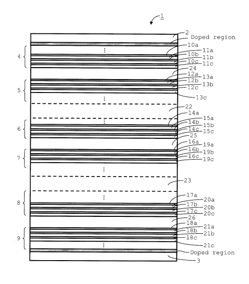
A photovoltaic cell 1 is shown in Fig. 1 only insofar
as necessary for illustrating the invention. In an actual
photovoltaic device, the photovoltaic cell 1 would be
encapsulated in further layers, including one or more layers of
plastic foil for sealing the photovoltaic cell from the
environment and/or sheets of glass. In the illustrated
embodiment, the photovoltaic cell 1 is a tandem cell, i.e. a
stack of component cells. In this case, the individual cells in
the stack are electrically connected in series. Parallel
connection is an alternative, but more complicated.
The illustrated photovoltaic cell 1 is a two-terminal
device, and includes a top electrode 2 and a back electrode 3.
CA 02632098 2008-05-28
WO 2007/063102 7 PCT/EP2006/069140
The top electrode is made of a transparent conducting material,
for example Sn02 (tin oxide), ITO (indium tin oxide), ZnO (zinc
oxide), Zn2SnO4 (zinc stannate), Cd2SnO4 (Cadmium stannate) or
InTiO (Indium Titanium oxide). The back electrode 3 is at least
partly made of a metal, such as Al (aluminium) or Ag (silver), a
metal alloy or a transparent conducting material. In an
embodiment, the back electrode 3 is made of a combination of a
metal and a transparent conducting material, the former being
situated towards the outside of the photovoltaic cell 1.
The photovoltaic cell 1 in the embodiment of Fig. 1
comprises semiconducting regions 4-9. In other embodiments,
there may be fewer or more of such regions. Of each pair of
semiconducting regions, one functions as an efficient transport
region for electrons and the other is arranged to function as an
efficient transport region for holes.
In the embodiment of Fig. 1, each of the semiconducting
regions 4-9 comprises a superlattice. Semiconductors based on
superlattices are known in the art. In the present text, the
term superlattice will be used to denote both known variants:
those comprising layers of a first material interspersed with
layers of a second material, both being sufficiently thin to
affect the band gap and those wherein nanocrystals are formed
from an semiconducting layer, where the size of the
nanocrystals, or quantum dots, affect the effective band gap of
the superlattice. An example of the latter kind of superlattice
is set out more fully in Green, M.A., "Silicon nanostructures
for all-silicon tandem solar cells", 19th European Photovoltaic
Solar Energy Conference and Exhibition, Paris, June 7th-llth,
2004. Superlattices of the layered kind are comprised in the
embodiment described herein in more detail.
The layered superlattices comprise a periodically
repeating combination of a layer of a low band gap semiconductor
material, called the well, with a layer of a wide band gap
material, called the barrier. Thus, in Fig. 1, a first
semiconducting region 4 includes a repeating combination of
first barrier layers l0a-lOc and first well layers lla-llc. A
second semiconducting region 5 includes a repeating combination
of second barrier layers 12a-12c and second well layers 13a-13c,
whereas a third semiconducting region 6 includes a repeating
CA 02632098 2008-05-28
WO 2007/063102 8 PCT/EP2006/069140
combination of third barrier layers 14a-14c and third well
layers 15a-15c. Fourth, fifth and sixth semiconducting
regions 7-9 include fourth, fifth and sixth barrier
layers 16a-16c, 17a-17c and 18a-18c, respectively, alternating
with fourth, fifth and sixth well layers 19a-19c, 20a-20c and
21a-21c, respectively. The values of the thickness of the
layers 10-21 lie in the range of 1-2 nm, at least below 10 nm.
Each of the semiconducting regions 4-9 has a total thickness in
the order of a hundred nm, at least below 200 nm.
The layers 10-21 of the present example are made of
hydrogenated or fluorinated amorphous semiconducting materials.
Suitable examples include hydrogenated amorphous silicon (a-
Si:H), hydrogenated amorphous silicon germanium (a-SiGe:H),
hydrogenated amorphous silicon carbide (a-SiC:H), hydrogenated
amorphous silicon nitride (a-SiN:H) and hydrogenated amorphous
silicon oxide (a-SiO:H). The band gap of a-Si:H depends on the
deposition conditions and varies from 1.6 eV to 1.9 eV. Alloying
a-Si:H with carbon, oxygen or nitrogen widens the band gap of
the alloys, whereas incorporating germanium lowers the band gap.
Suitable embodiments can be made by using a-Si:H and a-SiGe:H as
material for the wells, i.e. the well layers 11,13,15,19,21 and
using a-SiC:H, a-SiN:H or a-SiO:H as material for the barriers,
i.e. the barrier layers 10,12,14,16,18. The non-periodic
structure of a-Si:H based layers and the ability of hydrogen to
passivate coordination defects eliminate the stringent
requirements for lattice matching that apply to crystalline
superlattices.
To form the superlattices, one or more of several
techniques may be used. These techniques include chemical vapour
deposition, reactive (co-) sputtering, reactive (co-)
evaporation, etc. To manufacture the illustrated example, an
advantageous technique is Plasma Enhanced Chemical Vapour
Deposition (PECVD). This technique is advantageous because the
alloying of a-Si:H can be accomplished easily by adding
appropriate gases to the silicon carrying source gas such as
silane. It has been demonstrated that superlattices can be
fabricated that are neither lattice matched nor epitaxial, yet
with interfaces that are essentially free of defects and nearly
atomically sharp.
CA 02632098 2008-05-28
WO 2007/063102 9 PCT/EP2006/069140
The adjacent semiconducting regions 4-9 of different
pairs are separated by tunnel-recombination junctions 22,23 that
include N-type and P-type regions. The tunnel-recombination
junctions 22,23 provide for the internal series connection,
where the recombination of oppositely charged carriers arriving
from the adjacent pairs of semi-conducting regions takes place.
Tunneling of the carriers through the layers forming the tunnel-
recombination junction facilitates the recombination. The
effective recombination of the photo-generated carriers takes
place through the defect states in the centre of the junction.
The recombination of the photo-generated carriers in the centre
of the junction keeps the current flowing through the solar
cell.
Of each pair of semiconducting regions, one is arranged
to function as an efficient transport region for holes and the
other as an efficient transport region for electrons. In the
illustrated embodiment of Figure 1, the superlattices are
attached to an N-type semiconductor region and a P-type
semiconductor region, i.e. doped semiconductor regions that form
a part of the tunnel recombination junctions 22,23. It is noted
that the doped regions may also comprise superlattices.
As is well known, the space charge in the differently
doped semiconductors generated due to the out-diffusion of
majority charge carriers from the doped layers gives rise to an
internal electric field. This brings about a separation of
mobile charge carriers created by excitation. The combination of
the first and second semiconducting regions 4,5 converts solar
energy in a first range of the solar spectrum, the combination
of the third and fourth semiconducting regions 6,7 converts a
second, different but possibly overlapping region of the solar
spectrum, and the combination of the fifth and sixth
semiconducting regions 8,9 yet another range. The tunnel
recombination junctions 22,23 ensure that the three pairs of
semiconducting regions are electrically connected in series.
The semiconducting regions 4-9 have progressively
decreasing effective band gaps. Thus, a first and second
semiconducting region 4,5 have a larger effective band gap, so
as to capture photons in a higher (frequency) range of the solar
spectrum. Intermediate semiconducting regions 6,7 have an
CA 02632098 2008-05-28
WO 2007/063102 10 PCT/EP2006/069140
effective band gap in an intermediate range of the solar
spectrum. Lower semiconducting regions 8,9 have an effective
band gap in a lower range of the solar spectrum. The top
semiconducting regions 4,5 are situated nearest the top
electrode 2. The top electrode 2 is exposed to incoming light,
in use, which thus passes through the semiconducting regions 4-9
in order of decreasing effective band gap. This configuration
provides improved efficiency of solar energy conversion, due to
suppression of thermalisation of charge carriers.
As a result of the incorporation of respective first,
second and third absorption layers 24-26 of materials for
absorption of radiation in between the top, intermediate and
lower pairs of semiconducting regions 4-9, absorption of
incident radiation is largely accounted for by the absorption
layers. Consequently, the thickness of the semiconducting
regions can be limited by reducing the amount of well layers and
barrier layers which is advantageous from a manufacturing
perspective. The absorption layers 24-26 of materials for
absorption of radiation adjoin the respective superlattices
forming a pair. They are of such a thickness that the excitation
levels are determined by their composition. Suitable values for
the thickness are in a range about fifty nm, preferably in a
range about ten nm.
The absorption layers 24-26 may comprise a direct
semiconductor material. Such a material has a relatively high
absorption coefficient of 104 to 106 cm-1 so that the absorption
layers 24-26 can be kept thin. For example CdS with a band gap
of 2.45 eV has the absorption coefficient at 500 nm around 105
cml, Cu(In,Ga)(Se,S)2r which band gap can be varied in a broad
range from 1.0 to 1.7 eV having in this energy range an
absorption coefficient between 104 to 105 cm-l. Absorption
involves the excitation of electrons from the valence to the
conduction band. Relatively high absorption coefficients also
characterise an alternative, namely organic molecular materials.
Such materials are used in the example described herein. In
organic molecular materials, the excited charge carriers are
commonly referred to as excitons. Suitable organic molecular
materials include porphyrins and phtalocyanines. These have
narrow absorption bands around frequencies corresponding to a
CA 02632098 2008-05-28
WO 2007/063102 11 PCT/EP2006/069140
photon energy level of about 2.9 eV and 1.77 eV, respectively.
Phtalocyanine molecules in particular are chemically very stable
and can be deposited by vacuum evaporation. The excitation
levels of the materials in the absorption layers 24-26 are
selected to allow them to match the effective bands of the
adjoining superlattices. As the band gaps of these can be
engineered through the dimensions of the thin layers 10-21, such
matching can be achieved with a relatively high degree of
accuracy.
Charge carriers in the absorption layers 24-26 are
excited to a level at or above the lower boundary of the
effective conduction band of the adjoining superlattice. This
allows for transfer of charge carriers to the superlattice with
relatively high efficiency. The efficiency is high due to the
low thermalisation losses that are incurred when the charge
carriers are transferred to the conduction band. Matching is
preferably accurate to a value in the range of tenths of an
electronvolt, e.g. 0.1 or 0,2 eV. In a molecular material, the
charge carriers are excited to the Lowest Unoccupied Molecular
Orbital (LUMO), which thus matches the lower boundary of the
effective conduction band of the adjoining superlattice.
Preferably the state from which the charge carrier is excited -
this state is called the Highest Occupied Molecular
Orbital (HOMO) in a molecular material for absorbing radiation -
matches the effective valence band, at least its upper bound, to
the same degree of accuracy.
Fig. 2 illustrates the general concept of the
photovoltaic cell 1 by means of an energy diagram. First and
second absorbing layers 27,28 adjoin parts of
superlattices 29-32. The superlattices 29-32 have substantially
the properties of intrinsic semiconducting materials. They form
energy selective transport layers, having a conduction or
valence band substantially matched to the stable or excitation
level of the adjacent absorbing layer 27,28. In fact, as
illustrated in Fig. 2, the conduction bands of the superlattices
30, 32 are slightly beneath the excitation levels of the
adjacent absorption layers 27, 28, whereas the valence bands of
the superlattices 29, 31 are slightly above the stable levels of
the adjacent absorbing layers 27, 28.
CA 02632098 2008-05-28
WO 2007/063102 12 PCT/EP2006/069140
Parts of a superlattice 30 adjoining the first
absorbing layer 27 and of a superlattice 31 adjoining the second
absorbing layer 28 form semiconducting regions having different
effective band gaps. Whether a part of one of the
superlattices 29-32 functions as an effective transport of
electrons or holes is determined by the nature of the adjacent
semiconducting region of one of three tunnel-recombination
junctions 33-35. The tunnel recombination junctions 33-35 each
comprise a pair of semiconducting layers, one of which is doped
to make it a P-type semiconducting layer, the other to make it
an N-type semiconducting layer. The function of the tunnel
recombination junctions is to provide a series connection
between the respective superlattices 29-32 with integrated
absorbing layers 27,28, and to set up an internal electric field
within the active region of the photovoltaic cell 1.
Fig. 3 illustrates a variant of the general concept of
Fig. 2 of the photovoltaic cell 1 by means of an energy diagram.
Again, first and second absorbing layers 27,28 adjoin parts of
superlattices 29-32. However, the superlattices 29-32 of a
single pair are different in the embodiment of Fig. 3. The
superlattices 29-32 are selected to have different effective
band gaps within a pair. The band gaps are engineered such that
negative charge carriers, excited in the superlattice 29, are
forced towards the tunnel-recombination junction 34, whereas
positive charge carriers, excited in the superlattice 30, are
driven towards the tunnel-recombination junction 33.
Fig. 4 shows a production line 36 for manufacturing an
array of solar cells with the configuration of the solar cell 1
that has been described. The production line 36 in the example
comprises two stations 37-38, past which a length of foil is
advanced. The array of solar cells is formed on the foil as it
is transferred from a first roll 39 to a second roll 40. The two
stations 37,38 are exemplary only, as there could be more of
them. In particular where PEVCD is used, solar cells can be
produced very efficiently by forming the layers 10-21, 24-26 in
succession at one or more stations 37,38 which are positioned
along the foil path. Patterning, using a laser or other cutting
technique, is applied to form the individual cells. Due to the
use of the first and second rolls 38,39, quasi-continuous
CA 02632098 2008-05-28
WO 2007/063102 13 PCT/EP2006/069140
production, limited primarily by the maximum practicable
diameter of the rolls 39,40, is made possible. Arrays of a
suitable size can be formed from the length of foil after
further processing, such as the application of plastic
protective layers, the removal of a backing layer, etc. The
array is then incorporated into a photovoltaic device including
suitable connectors and optional additional circuitry. The use
of units of spectrum-selective absorbing materials in
conjunction with superlattices with effective band gaps
engineered to match the absorption bands of the material,
especially in a tandem cell configuration, makes the
photovoltaic device efficient and relatively uncomplicated to
produce.
The invention is not limited to the embodiments
described above, which may be varied within the scope of the
accompanying claims. For instance, the absorption bands of the
materials for absorption of radiation may overlap partially.
Also, embodiments are possible wherein one of each pair of
semiconducting regions adjoining a layer for spectrum-selective
absorption of radiation is made of an inorganic, direct or
indirect, semiconducting material, instead of comprising a
superlattice. Furthermore, the pairs of semiconducting regions
forming a multi-junction cell may be separated by layers of
inorganic semiconducting material, or such a layer may be
provided in between an electrode and a superlattice.