Note: Descriptions are shown in the official language in which they were submitted.
CA 02632645 2008-06-06
WO 2007/056730 PCT/US2006/060622
VARIABLE PASSIVE COMPONENTS WITH HIGH RESOLUTION VALUE
SELECTION AND CONTROL
CROSS-REFERENCE TO RELATED APPLICATIONS
This application claims the benefit of U.S. provisional patent application
number
60/734,516, filed November 7, 2005, which is herein incorporated by reference
in its
entirety.
BACKGROiJND
A portion of the disclosure of this patent document contains material that is
subject to copyright protection. The copyright owner has no objection to the
facsimile
reproduction by anyone of the patent document or the patent disclosure, as it
appears in
the Patent and Trademark Office patent files or records, but otherwise
reserves all
copyright rights whatsoever.
1. FIELD
The present system relates to the field of variable, passive, electronic
components.
2. BACKGROUND ART
Throughout the history of electronics, the inherent characteristics and
consequences associated with the presence of fixed value passive components
have
impacted circuit perfonnance. The characteristics include component
tolerances,
tolerance build-up, the relatively high cost of using high precision
components, added
circuitry required to provide precision control or precisely set component
values or
performance characteristics, and changes in component value or performance
produced
by component aging, operating history, and changes in environmental
conditions.
Figure 1 illustrates an idealized solution in the form of variable resistor
R100,
varaiable capacitor C100 and variable inductor L100. These components would be
comparable in nature to the present passive devices they would replace, but
whose value
could be adjusted to provide nearly nominal performance over widely varying
operating
conditions. Variability would either be part of the manufacturing processes,
or
dynaniically available during actual operation, as determined on a case-by-
case basis.
CA 02632645 2008-06-06
WO 2007/056730 PCT/US2006/060622
One useful application illustrated is directed toward providing a matched,
complex
termination (Z100) for a transmission line structure (TL 100).
As a result of the long-recognized benefits associated with use of variable
passive
components, techniques have been made developed to provide this capability
using the
present art. The effectiveness of the techniques is generally limited to
specific types of
components over a limited range of operating conditions, such as frequency or
power
level. One example of a digitally controlled, variable resistor of the present
art is shown
in Figure 2A. A switched resistor network is used with control FETs such that
turning
one or more FETs "on" places resistors in parallel, reducing the effective
resistive value
of the combination. Resistor networks are more frequently implemented as
series
structures with one or more FETs used to short out unwanted resistors in the
chain. For
resistors, value selection controls are far simpler with series connection.
Switched
capacitor structures are typically configured as parallel networks, again
simplifying value
selection controls.
Other implementations of variable value components generally realize the
function but can have significant impact on the circuit or limited
performance. Figure 2B
illustrates the use of the channel resistance of a FET as a variable resistor
(note resistor
R206 is variable implying some form of gate voltage control). Among the
undesirable
characteristics of this approach are the large number of unused components and
the
characteristics of the FET switches. When a value has been selected, there are
typically
many unused components. This is typically not a major issue for an integrated
resistor
network but switched capacitor networks can require discrete capacitors to
realize large
values, adding cost and using circuit board area that could be used for
functioning
circuitry.
The switch FETs also can present significant problems. If kept small to
minimize
chip area utilization, they tend to have significant resistance that is
aggravated by their
rapid resistance increase with temperature (a sensitivity experienced to an
even greater
degree by the circuit for Figure 2B). If the FETs are enlarged to reduce
resistance, they
consume greater area. Either way, there is an incentive to minimize the number
of
switched devices (4-bit is most common with 8-bit the maximum generally
encountered),
thereby limiting resolution of the component value.
2
CA 02632645 2008-06-06
WO 2007/056730 PCT/US2006/060622
Figure 2C illustrates a varactor diode, which provides the function of a
controlled
variable capacitor. Implementation requires a DC control voltage and DC
isolation. Use
is generally limited to RF applications where the small diode capacitance
under reverse
junction bias yields appropriate values for circuit operation.
Inductors are particularly difficult components in which to implement
variability
because they frequently are wound around a magnetic core material.
Modification of the
geometric relationship between the core material and the winding provides
inductance
adjustment capacity. However, the adjustment capacity is typically a
mechanical setting
with real time adjustment being largely impractical, particularly at high
frequencies.
A significant issue associated with realization of component value variability
is
energy storage, which is a fu.nction of the component value (whether primary
or parasitic
in nature). Alteration of a component value typically involves movement of
energy into or
out of the storage mechanisms associated with the specific type of passive
component,
thereby significantly limiting the speed of circuit operation. For many
applications, it
would be highly beneficial to be able to change the apparent component value
without
requiring significant energy transfer.
It would therefore be highly desirable to implement low cost, high-resolution
value variation for common passive components.
3
CA 02632645 2008-06-06
WO 2007/056730 PCT/US2006/060622
SUM'MARY
The present system is an electronic, digital-to-analog converter (DAC) circuit
that
provides means to detect current flowing through a passive component and
source or sink
additional current such that the value of the passive component appears to
vary from its
actual or fixed value. The term "fixed value" is not iritended to imply that
the passive
component value does not vary with environmental or circuit application
conditions, or
include initial tolerance variation. Rather than unchanging, the term "fixed
value" means
the instantaneous actual value of the component (or component characteristic)
in the
specific circuit and under the actual environmental conditions in which it is
operating.
The present system employs feedback such that the additional current tracks
current flowing through the passive component. The DAC functions as a source
for the
additional current and either supplies it directly or functions as a reference
for external
current drive circuits. The digital inputs to the DAC function to set the gain
of the DAC
and thereby provide high-resolution adjustment of the equivalent variable
component
value. Resolutions equal to or greater than 24-bits may be realized, where the
resolution
is primarily limited by the combined DAC operating frequency and resolution in
each
specific application.
In one or more embodiments, the present system is coupled to a fixed value
passive component within an electronic circuit, whereby operation of the
present system
produces operation by the electronic circuit substantially equivalent to that
which would
be produced by an altered value of the fixed value passive component.
In one or more embodiments of the present system, the value of the fixed value
passive component is a linear component.
In one or more embodiments of the present system, the value of the fixed value
passive component is a non-linear component.
In one or more embodiments of the present system, the fixed value passive
component is a characteristic of an active component such as a semiconductor
junction
capacitance.
In one or more embodiments of the present system, a transimpedance amplifier
senses the current through the fixed value passive component.
4
CA 02632645 2008-06-06
WO 2007/056730 PCT/US2006/060622
In one or more embodiments of the present system, the output of the
transimpedance amplifier is coupled to a DAC voltage reference input.
In one or more embodiments, the present system includes a current sense
resistor
in series with the fixed value passive component.
In one or more embodiments of the present system, the feedback signal from the
current sense resistor coupled to a DAC voltage reference input.
In one or more embodiments, the present system includes a DAC that directly
sources or sinks current from the circuit nodes terminating the series
combination of the
fixed value passive component and the current sense resistor.
In one or more embodiments, the present system includes a DAC that provides
reference current for external drive circuitry that sources or sinks current
from circuit
nodes terminating the series combination of the fixed value passive component
and the
current sense resistor.
In one or more embodiments, the present system includes external drive
circuitry
with single sided current sense and single output for driving a shunt passive
component
with current sense resistor connected to ground.
In one or more embodiments, the present system includes external drive
circuitry
with differential current sense and differential outputs for driving a series
passive
component with floating current sense resistor.
In one or more embodiments, the present system includes external drive
circuitry
for high current applications, including one or more output current amplifiers
having both
differential inputs and differential outputs.
In one or more embodiments of the present system, the fixed value passive
component is a distributed structure such as a transmission line, resonant
cavity, slotted
line, stub tuner, waveguide or antenna.
In one or more embodiments of the present system, more than one DAC controls
current injection or removal from a single pair of nodes.
In one or more embodiments of the present system, current sense feedback is
taken from a passive component connected between nodes into which current is
neither
injected nor removed in response to the current sense feedback.
5
CA 02632645 2008-06-06
WO 2007/056730 PCT/US2006/060622
In one or more embodiments of the present system, the present system provides
signals that are coupled between two or more fixed value passive components.
In one or more embodiments, one or more variable components of the present
system are varied as a function of frequency such that the circuit functions
as a tracking
filter.
6
CA 02632645 2008-06-06
WO 2007/056730 PCT/US2006/060622
BRIEF DESCRII'TION OF THE DRAWINGS
Figure 1 is an illustration of a number of variable passive components
realizable
by various embodiments of the present system.
Figure 2A is a circuit diagram of a switched resistor network.
Figure 2B is a circuit diagram of a FET realization of a variable resistor.
Figure 2C is a circuit diagram of a varactor diode realization of a variable
capacitor.
Figure 3A is a circuit diagram of a fixed value, series resistor.
Figure 3B is a circuit diagram of a fixed value, shunt resistor to ground.
Figure 3C is a circuit diagram of the resistor of Figure 3A incorporating a
resistive
embodiment of the current sense function of the present system.
Figure 3D is a circuit diagram of the resistor of Figure 3B incorporating a
resistive
embodiment of the current sense function of the present system.
Figure 3E is a circuit diagram of the circuit of Figure 3C with the fixed
value
resistor replaced by a fixed value capacitor.
Figure 3F is a circuit diagram of the circuit of Figure 3D with the fixed
value
resistor replaced by a fixed value capacitor.
Figure 3G is a functional block diagram of one embodiment of the present
system.
Figure 3H is a functional block diagram of one embodiment of the present
system
with floating current sense resistor.
Figure 31 is a functional block diagram of the preferred embodiment of the
present
system incorporating zero impedance current sense.
Figure 3J is a simplified circuit diagram of the transimpedance amplifier
function
shown in Figure 31.
Figure 4A is a circuit diagram illustrating use of variable component value to
control output signal amplitude.
Figure 4B is a circuit diagram illustrating means for realization of the
component
variability as illustrated in Figure 4A.
7
CA 02632645 2008-06-06
WO 2007/056730 PCT/US2006/060622
Figure 4C is a circuit diagram illustrating alternate means for realization of
component variability as illustrated in Figure 4B.
Figure 5A is a circuit diagram of a single output embodiment of the present
system.
Figure 5C is a circuit diagram of a differential output embodiment of the
present
system.
Figure 6 is a functional block diagram of a variable resistor embodiment of
the
present system.
Figure 7 is a functional block diagram of a variable resistor embodiment of
the
present system with alternate current feed polarity.
Figure 8 is a functional block diagram of a variable resistor embodiment of
the
present systein with fine adjustment capability.
Figure 9 is a fun.ctional block diagram of a high current, variable resistor
embodiment of the present system.
Figure 11 is a functional block diagram of the present system illustrating
open
loop signal coupling from a second passive component to a first, variable
passive
component.
Figure 12 is an illustration of the RF frequency characteristics of a tracking
filter
embodiment of the present system.
Figure 13 is an illustration of the IF frequency characteristics of a tracking
filter
embodiment of the present system.
Figure 14 is a functional block diagram of a generic receiver system employing
conventional filters.
Figure 15 is a functional block diagram of the generic receiver system of
Figure
14 implemented with multiple tracking filter embodiments of the present
system.
8
CA 02632645 2008-06-06
WO 2007/056730 PCT/US2006/060622
DETAILED- DESCRIPTION OF THE SYSTEM
The present system is directed to variable passive components with high-
resolution, digital value selection and control. In the following description,
numerous
specific details are set forth to provide a more thorough description of
embodiments of
the system. It is apparent, however, to one skilled in the art, that the
system may be
practiced without these specific details. In other instances, well known
features have not
been described in detail so as not to obscure the system. Except as noted
herein, common
components and connections, identified by common reference designators
function in like
manner in each circuit.
The present system is a digital-to-analog converter circuit that provides the
capability to dynamically vary the apparent value of passive components to the
circuitry
to which they are coupled in a wide range in analog and mixed signal
electronic circuits.
The term "fixed value" refers to does not imply that the value of the
component does not
vary with operating or environmental conditions, but rather represents the
component
value while operating in the circuitry without operation of the present system
to alter its
apparent value. The term "passive components" represents either individual
discrete
passive parts or passive characteristics of other components such as diodes,
bipolar
junction 'transistors, FETs, etc. The passive components may be linear or non-
linear.
A consideration in implementation of the present system is whether or not the
passive component has one of its terminals connected to ground (or either a
floating
reference or return node). Ground connected components are typically easier to
vary with
a wider choice of implementations than for an arbitrarily connected passive
component.
One element of the present system is a means for sensing the current flowing
through the fixed value passive component whose apparent value is to be
varied. One
example means of current sensing is by the addition of a small value, current
sense
resistor placed in series with the passive component. Figures 3A through 3F
illustrate
some of the various configurations of passive components, each with current
sense
resistors added in series.
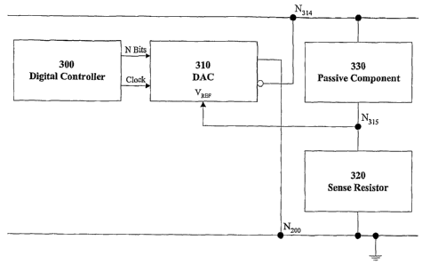
One embodiment of the present system is illustrated in Figure 3G. DAC310 is a
current output DAC with a voltage reference input VREF. Current sense resistor
320 is
9
CA 02632645 2008-06-06
WO 2007/056730 PCT/US2006/060622
placed in series with a fixed value passive component 330. The voltage across
resistor
320 is a representation of the current through passive component 320 and is
applied to the
reference input of DAC 310. Within the bandwidth of the DAC reference
amplifier, the
output current maintains the same characteristic shape as a function of time,
as that
through the fixed value passive component. Thus the output of the DAC is
equivalent to
a fixed value passive component of the same type as passive component 330
placed in
parallel with passive component 330. The value of the "added parallel
component" is
determined by scaling of the DAC output current by the DAC digital input
setting. For
some applications, the apparent value of the fixed value component can be
altered intra-
cycle up to some frequency.
As shown in Figure 3G, the DAC outputs are cross coupled such that positive
DAC output current flows in the same direction as a positive current through
the sense
resistor. If the passive component is a capacitor, the configuration shown
would make the
capacitor appear larger in value. If the passive component is a resistor or
inductor, the
apparent parallel combination would be a smaller value. If the positive and
negative
outputs of the DAC are swapped, as shown in Figure 8, the capacitor value
would
apparently decrease and that of a resistor or inductor increase. Thus, the
present system
can readily produce negative component values. The value change is of course
dynamic
in nature and does not provide energy storage.
Figure 3H illustrates an altemate embodiment with floating current sense
resistor.
The embodiment of Figure 3G has 3 is typically used for components that are
coupled to ground. An embodiment for use with non-grounded components is
discussed
below. Note that the addition of any resistance in series with passive
component 330 can
impact circuit performance for some applications. One alternative is discussed
in the
Transimpedance Amplifier Current Sense Embodiment below. Further, DACs are
typically not designed for this type of application and operate using a DC
voltage
reference. As a result, the bandwidth of the reference input amplifier may be
limited
(around 500KHz). However, in some of the newer DACs, this bandwidth is l Os of
MHz.
The embodiment for floating components provides a direct means for avoiding
the
reference amplifier bandwidth limitation and implementing the present system
at RF
frequencies.
Transimpedance Amplifier Current Sense Embodiment
CA 02632645 2008-06-06
WO 2007/056730 PCT/US2006/060622
Figures 31 and 3J illustrate a method for sensing the current in shunt
components
to ground when feasible. Within the bandwidth of the transimpedance amplifier,
the
current is sensed while the passive component terminal is held at virtual
ground. Use of
the transimpedance amplifier avoids performance degradation caused by the
presence of a
current sense resistor or any offset voltage associated with the DAC reference
amplifier
that may or may not be easily correctable.
Wideband transimpedance amplifiers are realizable with appropriately designed
feedback. It is desirable to have the transimpedance amplifier circuitry
integrated into the
DAC integrated circuit with external feedback selection by the user. Figure 3J
illustrates
an embodiment of a transimpedance apmplifier 350.
Variable Component Equivalent Circuit
Figure 4A is a schematic that illustrates one of the methods for the use and
implementation of a variable component. VSOURCEI is a voltage source
generating an
arbitrary output waveform at node N40 1. Output voltage VO at node N402 is a
reduced
amplitude representation of the voltage at node N40 1. The amplitude reduction
is
produced by a resistor divider network comprised of resistor R401 coupling
node N401 to
node N402 and a resistor equivalent comprised of the parallel combination of
resistors
R402 and R403, which couple node N402 to ground. Resistor R402 is variable and
is
used to compensate for variations in the values of resistors R401 and R403,
thereby
providing the desired ratio of the voltages at nodes N401 and N402. The
current flowing
through resistor R402 is IR402.
An equivalent circuit for maintenance of the ratio of voltages at nodes N401
and
N402 is shown in Figure 4B. A second voltage source VSOURCE2 couples node N403
to ground and is connected in series with resistor R404, which couples node
N403 to node
N402. Voltage source VSOURCE2 and resistor R404 operate together such that the
current through resistor R404 is IR402, the same as the current flowing
through resistor
R402 of Figure 4A. Thus the combination of voltage source VSOURCE2 and
resistor
R404 is the functional equivalent of the variable resistor R402. Typically,
the output of
voltage source VSOURCE2 will be variable and the value of resistor R404 will
be fixed.
Figure 4C is an alternate representation to the circuit shown in Figure 4B.
Current
source ISOURCE2 couples node N402 to ground and replaces the series
combination of
11
CA 02632645 2008-06-06
WO 2007/056730 PCT/US2006/060622
voltage source VSOURCE2 and resistor R404. The current supplied is IR402 so
that the
current source is the functional equivalent of variable resistor R403 in
Figure 4A. For the
embodiments illustrated in Figures 3G, 3H, 31, 6, 7, 8, 10, and 11, current
source
ISOURCE2 is provided directly by the output from a current output DAC. For the
embodiment illustrated in Figure 9, current source ISOURCE2 is provided by the
combination of current output DAC DAC310 and current amplifier 900A.
Embodiment for Generic Passive Component Value Selection
As previously discussed, presently available DACs are often of limited use for
the
embodiment illustrated in Figure 3G and the transimpedance amplifier
embodiment
illustrated in Figure 31. This can be due to the limited bandwidth of the
analog reference
input. While some devices have a reference bandwidth of several MHz, most are
limited
to approximately 500KHz. For the present system, this would limit their
utilization to
audio applications or equivalent.
The embodiments illustrated in Figures 5A and 5C represent embodiments for
realization of the highest level of speed and performance while avoiding the
DAC
reference limitations. These embodiments use the DAC in a configuration to set
the gain
of a differential amplifier. The differential amplifier functions as the input
or sense
element.
Figure 5A shows a single-ended version for use with components in shunt to
ground. Figure 5C shows the more general double-ended circuit to be used with
components between 2 arbitrary circuit nodes. The circuit of Figure 5C can
also be used
with ground reference in place of that shown in Figure 5A. Both of these
configurations
have the additional advantage of avoiding the problem with limited bandwidth
for the
reference input. Each has a high speed, differential amplifier input circuit
that allow
standard DACs to be used with a DC reference level, typically ground. The
configuration
shown in Figure 5A is a single output version of the configuration of Figure
5C.
High Current Embodiment
In addition to limited bandwidth of the reference input, another problem in
using
DACs of the present art is their limited output current capability. Many
variable
component applications simply require higher current levels than the 20
milliamperes that
is the typical maximum output for most DACs. One solution to the current
capacity
12
CA 02632645 2008-06-06
WO 2007/056730 PCT/US2006/060622
problem would be to simply increase the current output capability of the DAC.
However,
this approach can only be used to achieve a limited increased before it would
affect the
nature and realization of the DAC integrated circuit and its functionality.
Nevertheless,
variable component values can be as valuable in high current power circuits as
in low
power digital processing and communications applications.
A general solution involves the addition of a differential current amplifier
to the
output of the control DAC as shown in Figure 9. The positive output of DAC
DAC310 is
coupled to the positive input of differential current amplifier 900A. The
negative output
of DAC DAC3 10 is coupled to the negative input of differential current
amplifier 900A.
The positive output of current amplifier 900A is coupled to resistor R602 at
node N30 1.
The negative output of current amplifier 900A is coupled to ground at node
N200. As
with previous configurations, the outputs of current amplifier 900A can be
swapped with
the negative output coupled to node N301 and the positive output coupled to
ground at
node N200, as long as the corresponding change is made to the digital input to
DAC
DAC310.
For high current applications, use of current amplifier 900A may be required.
For
moderately higher current applications up to a few amperes, the need for
separate current
amplifier 900A can be avoided by of an alternate embodiment. Two forms of such
alternate embodiment are illustrated in Figures 5A and 5C implemented with
single high
current or multiple lower current output circuits, formed by the push-pull
current mirrors.
Use of the alternate embodiments of Figures 5A and 5C to resolve the problem
of limited
DAC current capability has the added advantage of simultaneously avoiding the
problem
of the limited bandwidth of the reference input previously described.
Component Value Selection Using Multiple Controls
Figure 11 illustrates a configuration wherein two separate DACs are used to
vary
a single component. Strictly speaking, this configuration alters the wave
shape of the
current flowing through the passive component 330A being varied such that it
may no
longer look like the same type of passive component. This may be mitigated if
passive
component 330B is the same type as 330A.
Use of this configuration is not likely to be a common occurrence since
typically
calibration routines controlled by Digital Controller 300 can accomplish the
same results
13
CA 02632645 2008-06-06
WO 2007/056730 PCT/US2006/060622
as an added mixed-signal circuit. The use of multiple controls has much
greater potential
for coupling signals into a single circuit.
Real Time Frequency Tracking Circuit Embodiments
A wide variety of electronic circuits either generate or are selectively
responsive
to different frequency signals. Examples are variable frequency oscillators or
filters.
Virtually any channelized system uses one or more tunable filters. Tuning
requires either
mechanical movement of a tuning element or use of a dynamically tracking
device.
Exarnples of the dynamically tracking devices include phase locked loops or
devices that
are able to affect the value of the reactance in a network. An example of the
latter type of
the device can include a varactor diode that functions to tune the effective
resonant
frequency of a transmission line or cavity.
Historically, there have been a number of approaches to deal with the basic
problem of differentiating a desired signal from the adjacent signals and
noise sources.
Figure 12 illustrates a signal within a passband. Under this condition, the
signal to noise
ratio is good and standard processing approaches are adequate. Figure 13
illustrates a
more typical situation, simplified to three ac signals. The signal at a
frequency below F1
is typically attenuated sufficiently such that it is not a problem unless it
has an
exceptionally large relative power. Of the two remaining signals inside the
passband
where the desired signal is the smaller of the two, a selection process should
occur or the
larger would dominate the detection process.
The typical selection process is illustrated in Figure 14. Selection is
accomplished
by mixing the broadband, amplified and filtered received signal with the
output of local
oscillator L01400 to generate the sum and difference frequencies. Filter F1402
follows
the mixer and is typically designed to both pass the difference frequency and
attenuate the
sum frequency.
One problem associated with this approach results from the fact that mixers
are
non-linear devices. If an interfering signal is sufficiently large, the mixer
is placed into
compression and the output amplitude of the smaller, desired signal is badly
attenuated.
The result is the need for very high 1P3 performance in the mixer with a
resulting reduced
ability to handle very small signals.
14
CA 02632645 2008-06-06
WO 2007/056730 PCT/US2006/060622
Figure 15 illustrates the embodiment of dynamically tunable filters in three
different locations. The ability to make input filters F1500 and F1501 narrow-
band
compared to those that typically'transmit the entire system passband,
substantially
reduces the interference from other signal/noise sources. For example, if the
tracking
filters have a bandwidth of 10% of the usual passband, the power of the
"noise" compared
to the desired signal power inside the passband of the tracking filter is
typically reduce by
a factor of 10, assuming a typical congested cell phone band as an example.
This
significantly reduces the IP3 requirements, reduces intermodulation products,
and allows
for better sensitivity of low amplitude signals. The use of a
tracking/adjustable filter
following the mixer allows for a much narrower band pass because the component
variations associated with manufacturing processes can be reduced to
insignificance.
A cascaded, double conversion process using two, offset IF frequencies is
commonly used to increase selectivity. Dynamically adjustable filters used
with the
cascaded selection improves the signal to noise ratio substantially beyond a
basic
approach as illustrated in Figure 15. Clearly these are a multitude of
reactive networks
used to filter or otherwise manipulate the frequency characteristics of such
systems. The
following discussion will be focused on the most simple, and easily
implemented form of
adjustable filter, the ground referenced parallel L-C network.
In order to maintain specific impedance for a filter, both the L and C
components
should be independently controlled. In general, this requires the use of two
DACs and
two feedback networks. By sensing and controlling both types of reactive
components it
is possible to control both the center frequency and the impedance of the
network at the
same time thereby allowing adjustable frequency and impedance control at any
given
frequency within the band. In special cases, two sense control currents maybe
fed back
by way of a single current buffer into a common node.
Another embodiment uses a single DAC and feedback circuit that affects the
performance of a network of components rather than an individual L or C. For
the series
LC tank circuit, one node is AC grounded and a signal is applied to the other.
This circuit
would function as a simple notch filter. It is well known that all components
have
parasitic resistance associated with them and this example has two. Applying
the DAC
and feedback system to the entire filter permits a reduction in the effective
parasitic
resistance of the network rather than varying the individual element values
and without
CA 02632645 2008-06-06
WO 2007/056730 PCT/US2006/060622
affecting the resonant frequency of the network. The result is a very high-
unloaded Q,
and a lower insertion loss for the network system. The lower loss and higher Q
permit
use of narrower filter bandwidth's and can also provide some of the benefits
associated
with super cooled circuits, lower thermal noise and greater frequency
selectivity. This
structure can be applied to more complicated network structures, to allowing
them to
more closely approach the functionality of ideal components than with present
circuit
structures. -
Thus, variable passive components with high resolution, digital value
selection
and control have been described.
16