Note: Descriptions are shown in the official language in which they were submitted.
CA 02632755 2014-02-10
Battery Protection and Zero-Volt Battery Recovery System
for an Implantable Medical Device
FIELD OF THE INVENTION
10021 The present invention relates generally to circuitry and techniques for
battery protection
and zero-Volt battery recovery preferably for use in an implantable medical
device such as an
implantable stimulator device, or more specifically an implantable pulse
generator.
BACKGROUND
10031 Implantable stimulation devices generate and deliver electrical stimuli
to body nerves and
tissues for the therapy of various biological disorders, such as pacemakers to
treat cardiac
arrhythmia, defibrillators to treat cardiac fibrillation, cochlear stimulators
to treat deafness,
retinal stimulators to treat blindness, muscle stimulators to produce
coordinated limb movement,
spinal cord stimulators to treat chronic pain, cortical and deep brain
stimulators to treat motor
and psychological disorders, and other neural stimulators to treat urinary
incontinence, sleep
apnea, shoulder sublaxation, etc. The present invention may find applicability
in all such
applications, although the description that follows will generally focus on
the use of the
invention within a Spinal Cord Stimulation (SCS) system, such as that
disclosed in U.S. Patent
No. 8,606,362.
10041 Spinal cord stimulation is a well-accepted clinical method for reducing
pain in certain
populations of patients. An SCS system typically includes an Implantable Pulse
Generator (IPG)
or Radio-Frequency (RF) transmitter and receiver, electrodes, at least one
electrode lead, and,
optionally, at least one electrode lead extension. The electrodes, which
reside on a distal end of
the electrode lead, are typically implanted along the dura of the spinal cord,
and the IPG or RF
transmitter generates electrical pulses that are delivered through the
electrodes to the nerve fibers
within the spinal column. Individual electrode contacts (the "electrodes") are
arranged in a
desired pattern and spacing to create an electrode array. Individual wires
within one or more
electrode leads connect with each electrode in the array. The electrode
lead(s) exit the spinal
column and generally attach to one or more electrode lead extensions. The
electrode lead
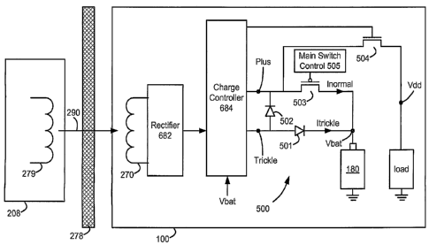
1
CA 02632755 2014-02-10
585-0002US1/ 05-01632-03
extensions, in turn, are typically tunneled around the torso of the patient to
a subcutaneous
pocket where the IPG or RF transceiver is implanted. Alternatively, the
electrode lead may
directly connect with the IPG or RF transceiver. For examples of other SCS
systems and other
stimulation systems, see U.S. Patents 3,646,940 and 3,822,708. Of course,
implantable pulse
generators are active devices requiring energy for operation, such as is
provided by an implanted
battery or an external power source.
[005] As should be obvious, an IPG needs electrical power to function. Such
power can be
provided in several different ways, such as through the use of a rechargeable
or non-rechargeable
battery or through electromagnetic (EM) induction provided from an external
charger, or from
combinations of these and other approaches, which are discussed in further
detail in U.S. Patent
6,553,263 ("the '263 patent"). Perhaps the favorite of these approaches is to
use a rechargeable
battery in the IPG, such as a lithium-ion battery or a lithium-ion polymer
battery. Such a
rechargeable battery can generally supply sufficient power to run an IPG for a
sufficient period
(e.g., a day or more) between recharging. Recharging can occur through the use
of EM
induction, in which EM fields are sent by an external charger to the IPG.
Thus, when the battery
needs recharging, the patient in which the IPG is implanted can activate the
external charger to
percutaneously (i.e., through the patient's flesh) charge the battery (e.g.,
at night when the patient
is sleeping or during other convenient periods).
10061 The basics of such a system are shown in Figure 1, which is largely
descriptive of salient
contents of the '263 patent. As shown, the system comprises in relevant part
the external charger
208 and IPG 100. As noted, a coil 279 in the charger 208 produces an EM
2
CA 02632755 2008-06-06
WO 2007/067825 PCT/US2006/060081
field 290 capable of percutaneous transmission through a patient's flesh 278.
The external
charger 208 may be powered by any known means, such as via a battery or by
plugging into a
wall outlet, for example. The EM field 290 is met at the IPG 100 by another
coil 270, and
accordingly an AC voltage is induced in that coil 270. This AC voltage is turn
is rectified to
a DC voltage at a rectifier 682, which may comprise a standard bridge circuit.
(There may
additionally be data telemetry associated with the EM field 290, but this
detail is ignored as
impertinent to the present disclosure). The rectified DC voltage is in turn
sent to a charge
controller 684, which operates generally to regulate the DC voltage and to
produce either a
constant voltage or constant current output as necessary for recharging the
battery 180. The
output of the charge controller 684, Le., how aggressively the charge
controller charges the
battery 180, is dependent on the battery voltage, Vbat, as will be explained
in further detail
later. (The charge controller 684 can also be used to report the battery 180's
charge status
back to the external charge 208 via back telemetry using coil 270, as
disclosed in the '263
application; however, because this function is not particularly relevant to
this disclosure, it is
not further discussed).
[007] The output of the charge controller 684 is in turn met by two switches
701, 702 which
respectively prevent the battery 180 from over-charging or over-discharging.
As shown,
these transistors are N-channel transistors, which will be "on," and thus
capable of
connecting the charge controller 684's output to the battery 180 when their
gates are biased.
Control of these gates is provided by a battery protection circuit 686, which
receives the
battery current and voltage, Ibat and Vbat, as control signals, again as will
be explained in
further detail later. For example, whenever the battery 180 exhibits too high
a voltage, the
battery protection circuit 686 will turn off the gate of the over-charging
transistor 701 to
protect the battery from further charging. A fuse positioned between the
transistors 701, 702
and the battery 180 may also be used to further protect the battery from very
high current
events (not shown). The battery 180 is coupled to one of several loads in the
IPG 100, such
as the electrode stimulation circuitry, i.e., the circuits the battery 180
ultimately powers. The
battery 180 is coupled to such loads through a load switch 504, which can
isolate the battery
180 from the load to protect one from adverse effects of the other. This load
switch 504 is
preferably part of the charge controller 684, which may comprise its own
integrated circuit,
although this is not strictly necessary.
[008] As discussed in the above-referenced '263 patent, the charging circuitry
684 can
charge the battery 180 in different ways, depending on the status of the
battery voltage, Vbat.
3
CA 02632755 2008-06-06
WO 2007/067825 PCT/US2006/060081
Without reiterating the contents of that disclosure, such selective charging
of the battery 180
is beneficial for safely charging the battery, particularly when a lithium-ion-
based battery is
used. Essentially, this safe charging scheme charges the battery 180 with
smaller currents
when the battery voltage Vbat is significantly depleted, and charges with
higher currents
when the battery voltage is still undercharged but at higher, safer levels.
[0091 Consider an embodiment in which Vbat = 4.2V represents a nominal voltage
for the
battery 180. When Vbat < 2.5V, the charge controller 684 will "trickle" charge
the battery
180 with a low level current, e.g., Ibat = 10 mA. As the battery charges and
as Vbat
increases, higher charging current can be used. For example, once Vbat > 2.5V,
a charging
current of That = 50 mA may be set by the charge controller 684. Once the
nominal voltage
of 4.2V is approached, the charge controller 684 may continue to charge the
battery 180 by
providing a constant voltage instead of constant current on its output, which
as charging
continues is manifest in a gradual decay of the battery current. The
relationship between
Vbat and That during battery charging is graphically illustrated in Figure 2.
Of course, these
various current and voltage values are merely exemplary, and other parameters
may be
suitable depending on the system at hand. Also, more than two levels of
charging current
(e.g., 10 mA, 25 mA, and 50 mA) can be used in stair-step fashion.
[00101 As noted earlier, the battery protection circuit 686 prevents the
battery from potential
damage during charging by disconnecting the battery from the charge controller
684.
Specifically, Vbat exceeds a safe value (e.g., greater than 4.2V), then the
over-charging
transistor 701 is disabled by the battery protection circuit 686 to block
further charging.
Likewise, if the battery voltage is less than a predetermined value and if
lbat exceeds a
predetermined value, over-discharge transistor 702 is disabled to prevent
discharging of the
battery. While disclosed as controlling two transistors 701, 702, the battery
protection
circuit 686 may control a single disabling protection transistor which
functions to disable the
battery 180 during both over-charging and over-discharging. Load switch 504
may be
similarly controlled to isolate the components to protect them from adverse
voltages and
currents.
[00111 While the charging and protection circuitry of Figure 1 is suitable,
its functionality
may be hampered at extremely low battery voltages. As the '263 patent
explains, this is
because the battery protection circuit 686 is powered by the battery voltage,
Vbat, and hence
when Vbat is extremely low (e.g., approaching zero Volts), the battery
protection circuitry
686 may not function as desired. In this regard, note that when Vbat is
extremely low, and
4
CA 02632755 2008-06-06
WO 2007/067825 PCT/US2006/060081
thus when the battery 180 is in need of charging, the battery protection
circuit 686 needs to be
able to turn transistors 701 and 702 on, else the charging controller 684 will
not be able to
pass a charging current, Ibat, to the battery. However, when Ibat is low, the
battery
protection circuit 686 may have difficulty generating a sufficient voltage to
turn on the gates
of the N-channel transistors 701 and 702. Specifically, the battery protection
circuitry 686
must be able to produce a gate voltage for the transistors that is greater
than Vgs (i.e., the
potential difference between the gate and source of the transistors). In
short, the battery
protection circuitry needs to be able to produce a gate voltage which exceeds
a threshold
voltage (Vt) of the transistors given the source voltages apparent at the
transistors. If Vbat is
below this threshold voltage, the battery protection circuit 686 may not be
able to produce a
suitably-high gate voltage to turn transistors 701 and 702 on.
[0012] Should this occur, the battery 180 cannot be charged, even though Vbat
is low and
hence the battery 180 is very much in need of charging. In other words, the
charging and
protection circuitry in Figure 1 is potentially susceptible to failure at when
Vbat is extremely
low, i.e., at zero Volts or near-zero Volts. In a worst case this would mean
that the IPG 100
is unrecoverable, and if implanted in a patient, may require the drastic step
of surgical
removal and replacement of the device. But this is unfortunate, because
patients in which
IPGs are implanted cannot necessarily be relied upon to diligently charge
their implanted
devices, and hence the risk of a depleted, unrecoverable battery is very real.
[0013] As a result, improved circuitry and techniques for protection and zero-
Volt recovery
for batteries in implantable medical devices would be beneficial. Such
solutions are provided
herein.
SUMMARY
[0014] Circuitry useable to protect and reliably charge a rechargeable
battery, even from a
zero-volt state, is disclosed, and is particularly useful when employed in an
implantable
medical device. The circuit includes two charging paths, a first path for
trickle charging the
battery at a relatively low current when the battery voltage is below a
threshold, and a second
path for charging the battery at relatively higher currents that the battery
voltage is above a
certain threshold. A passive diode is used in the first trickle-charging path
which allows
trickle charging even when the battery voltage is too low for reliable gating,
while a gateable
switch (preferably a PMOS transistor) is used in the second higher-current
charging path
when the voltage is higher and the switch can therefore be gated more
reliably. A second
CA 02632755 2008-06-06
WO 2007/067825 PCT/US2006/060081
diode between the two paths ensures no leakage to the substrate through the
gateable switch
during trickle charging. The load couples to the battery through the switch,
and preferably
through a second switch specifically used for decoupling the load.
BRIEF DESCRIPTION OF THE DRAWINGS =
[0015] The above and other aspects of the present invention will be more
apparent from the
following more particular description thereof, presented in conjunction with
the following
drawings wherein:
[0016] Figure 1 illustrates a prior art system comprising an external charger
for charging an
implantable pulse generator (IPG), and shows the charge controller and battery
protection
aspects of the IPG.
[0017] Figure 2 graphically shows the relationship between battery voltage and
battery
current during charging of the battery as dictated by the charge controller of
Figure 1.
[0018] Figure 3 shows a block diagram that illustrates exemplary implantable,
external, and
surgical components of a spinal cord stimulation (SCS) system that employs an
implantable
stimulator device in accordance with the present invention.
[0019] Figure 4 shows various components of the SCS system of Figure 1.
[0020] Figure 5 shows a block diagram that illustrates the main components of
one
embodiment of an implantable stimulator device in which the invention can be
used.
[0021] Figure 6 shows a block diagram that illustrates another embodiment of
an implantable
stimulator device in which the invention can be used.
[0022] Figure 7 is similar to the system illustrated in Figure 1, but includes
improved battery
protection and zero-Volt recovery circuitry in accordance with an embodiment
of the
invention.
[0023] Figure 8 illustrates the various sensors used in conjunction with the
improved
protection and zero-Volt recovery circuitry of Figure 7.
[0024] Figure 9 illustrates the main switch used in the improved protection
and zero-Volt
recovery circuitry of Figure 7, and shows parasitic current paths that can
exist.
6
CA 02632755 2008-06-06
WO 2007/067825 PCT/US2006/060081
DETAILED DESCRIPTION
[0025] The following description is of the best mode presently contemplated
for carrying out
the invention. This description is not to be taken in a limiting sense, but is
made merely for
the purpose of describing the general principles of the invention. The scope
of the invention
should be determined with reference to the claims and their equivalents.
[0026] Before discussing the battery protection and zero-Volt recovery aspects
of the
invention that is the focus of this disclosure, the circuitry, structure, and
function of an
implantable stimulator device in which thc disclosed circuitry and technique
can be used is
set forth for completeness with respect to Figures 3-6. The disclosed
implantable stimulator
device may comprise implantable pulse generator (IPG), or similar electrical
stimulator
and/or electrical sensor, that may be used as a component of numerous
different types of
stimulation systems. More specifically, the description that follows relates
to use of the
invention within a spinal cord stimulation (SCS) system as an exemplary
embodiment.
However, it is to be understood that the invention is not so limited. Rather,
the invention may
be used with any type of implantable electrical circuitry that could benefit
from improved
battery protection and zero-Volt recovery techniques. For example, the present
invention
may be used as part of a pacemaker, an implantable pump, a defibrillator, a
cochlear
stimulator, a retinal stimulator, a stimulator configured to produce
coordinated limb
movement, a cortical or deep brain stimulator, or in any other stimulator
configured to treat
urinary incontinence, sleep apnea, shoulder sublaxation, etc. Moreover the
technique can be
used in non-medical and/or non-implantable devices or systems as well, i.e.,
in any device or
system in which zero-Volt battery recovery and/or protection is necessary or
desirable.
[0027] Turning first to Figure 3, a block diagram is shown that illustrates
the various
components of an exemplary SCS system in which the invention may be used.
These
components may be subdivided into three broad categories: implantable
components 10,
external components 20, and surgical components 30. As seen in Figure 3, the
implantable
components 10 include an implantable pulse generator (IPG) 100, an electrode
array 110, and
(as needed) a lead extension 120. The extension 120 may be used to
electrically connect the
electrode array 110 to the IPG 100. In an exemplary embodiment, the IPG 100,
described
more fully below in connection with Figures 5 or 6, may comprise a
rechargeable, multi-
channel, telemetry-controlled, pulse generator housed in a rounded high-
resistivity titanium
alloy case to reduce eddy current heating during the inductive charging
process. The IPG 100
7
CA 02632755 2008-06-06
WO 2007/067825 PCT/US2006/060081
may provide electrical stimulation through a multiplicity of electrodes, e.g.,
sixteen
electrodes E1 through E16, included within the electrode array 110.
[0028] In this regard, the IPG 100 may include stimulating electrical
circuitry ("stimulating
electronics"), a power source, e.g., a rechargeable battery, and a telemetry
system, the latter
of which is particularly relevant to embodiments of the disclosed invention.
Typically, the
IPG 100 is placed in a surgically-made pocket either in the abdomen, or just
at the top of the
buttocks. It may, of course, also be implanted in other locations of the
patient's body. Once
implanted, the IPG 100 is connected to the lead system, comprising the lead
extension 120, if
needed, and the electrode array 110. The lead extension 120, for example, may
be tunneled
up to the spinal column. Once implanted and any trial stimulation period is
complete, the
lead system 110 and lead extension 120 are intended to be permanent. In
contrast, the IPG
100 may be replaced if it fails.
[0029] As seen best in Figure 4, and as also illustrated in Figure 3, the
electrode array 110
and its associated lead system typically interface with the implantable pulse
generator (IPG)
100 via the lead extension system 120 just mentioned. The electrode array 110
may also be
connected to an external trial stimulator 140, through the use of a
percutaneous lead
extension 132 and/or an external cable 134. The external trial stimulator 140
typically
includes the same or similar pulse generation circuitry as does the IPG 100,
and is used on a
trial basis, e.g., for 7-10 days, after the electrode array has been implanted
and prior to
implantation of the IPG 100, to test the effectiveness of the stimulation that
is to be provided.
[0030] Still with reference to Figures 3 and 4, and as noted earlier, a hand-
held programmer
(HHP) 202 may be used to control the IPG 100 via a suitable non-invasive
communications
link 201, e.g., an RF link. Such control allows the IPG 100 to be turned on or
off, and
generally allows stimulation parameters, e.g., pulse amplitude, width, and
rate, to be set by a
patient or clinician within prescribed limits. The HHP 202 may also be linked
with the
external trial stimulator 140 through another link 205', e.g., an infra red
link. Detailed
programming of the IPG 100 is preferably accomplished through the use of an
external
clinician's programmer (CP) 204 (Fig. 3), which may also be hand-held and
which may be
coupled to the IPG 100 directly via link 201a or indirectly through the HHP
202. An external
charger 208, non-invasively coupled with the IPG 100 through link 290, e.g.,
an inductive
link, allows energy stored or otherwise made available to the charger 208 to
be coupled into
the rechargeable battery 180 housed within the IPG 100, as explained in the
Background.
8
CA 02632755 2008-06-06
WO 2007/067825 PCT/US2006/060081
[0031] Turning next to Figure 5, a block diagram is shown that illustrates the
main
components of one embodiment of an implantable pulse generator (IPG) 100 in
which
embodiments of the invention may be used. As seen in Figure 5, the IPG
includes a
microcontroller (pC) 160 connected to memory circuitry 162. The ILIC 160
typically
comprises a microprocessor and associated logic circuitry, which in
combination with control
logic circuits 166, timer logic 168, and an oscillator and clock circuit 164,
generate the
necessary control and status signals which allow the tC 160 to control the
operation of the
IPG in accordance with a selected operating program and stimulation
parameters. (A
"microcontroller" as used herein should be understood as any integrated device
capable of
processing signals in the IPG, including traditional microcontrollers,
microprocessors, or
other signal processors, including those that are application-specific, such
as ASIC chips).
[0032] The operating program and stimulation parameters are telemetered to the
IPG 100,
where they are received via antenna 250 (which may include a coil 170 and/or
other antenna
components), processed, e.g., via RF-telemetry circuitry 172, and may be
stored, e.g., within
the memory 162. As noted earlier, the RF-telemetry circuitry 172 demodulates
the signal it
receives from the HHP 202 or CP 204 to recover the operating program and/or
the
stimulation parameters. More specifically, signals received by the antenna 250
are passed
through the transmit/receive switch 254 to amplifiers and filters 258. From
there, the
received signals are demodulated (262) using Frequency Shift Keying (FSK)
demodulation
for example, and the data is then sent to the microcontroller 160 for
processing and/or
eventual storage. When RF-telemetry circuitry 172 is used to transmit
information to the
HHP 202 or CP 204 to report in some fashion on its status, the microcontroller
160 sends
relevant data to transmission drivers 256, where the carrier is modulated by
the data and
amplified for transmission. The transmit/receive switch 254 would then be set
to
communicate with the transmission drivers 256, which in turn drive the data to
the antenna
250 to be broadcast.
[0033] The microcontroller 160 is further coupled to monitoring circuits 174
via bus 173.
The monitoring circuits 174 monitor the status of various nodes or other
points 175
throughout the IPG 100, e.g., power supply voltages, current values,
temperature, the
impedance of electrodes attached to the various electrodes Ei . . . EN, and
the like.
Informational data sensed through the monitoring circuit 174 may be sent to a
remote
location external to the IPG (e.g., a non-implanted location) through
telemetry circuitry 172
via coil 170.
9
CA 02632755 2008-06-06
WO 2007/067825 PCT/US2006/060081
[0034] The operating power for the IPG 100 may be derived from a rechargeable
power
source 180, which may comprise a lithium-ion or lithium-ion polymer battery,
for example,
as discussed earlier. The rechargeable battery 180 provides an unregulated
voltage to power
circuits 182. The power circuits 182, in turn, generate the various voltages
184, some of
which are regulated and some of which are not, as needed by the various
circuits located
within the IPG 100. In a preferred embodiment, the battery 180 is charged by
an
electromagnetic field created by an external portable charger 208 (Figs. 1, 3)
as already
noted. When placed near the IPG 100 (e.g., centimeters away), an
electromagnetic field
emanating from the portable charger 208 induces a current in charging coil 270
(even through
a patient's skin). This current is then rectified and regulated to charge the
battery 180, as
explained in the Background. Further associated with the charging circuitry is
charging
telemetry circuitry 272, which is used for example by the IPG 100 to report
back to the
portable charger 208 when the battery is full, and thus when portable charger
can be shut off.
[0035] In one exemplary embodiment, any of the N electrodes may be assigned to
up to k
possible groups or "channels." In one preferred embodiment, k may equal four.
Moreover,
any of the N electrodes can operate, or be included in, any of the k channels.
The channel
identifies which electrodes are selected to synchronously source or sink
current to create an
electric field in the tissue to be stimulated. Amplitudes and polarities of
electrodes on a
channel may vary, e.g., as controlled by the HHP 202. External programming
software in the
CP 204 is typically used to set parameters including electrode polarity,
amplitude, pulse rate
and pulse width for the electrodes of a given channel, among other possible
programmable
features.
[0036] The N programmable electrodes can be programmed to have a positive
(sourcing
current), negative (sinking current), or off (no current) polarity in any of
the k channels.
Moreover, each of the N electrodes can operate in a bipolar mode or multipolar
mode, e.g.,
where two or more electrode contacts are grouped to source/sink current at the
same time.
Alternatively, each of the N electrodes can operate in a monopolar mode where,
e.g., the
electrode contacts associated with a channel are configured as cathodes
(negative), and the
case electrode (i.e., the IPG case) is configured as an anode (positive).
[0037] Further, the amplitude of the current pulse being sourced or sunk to or
from a given
electrode contact may be programmed to one of several discrete current levels,
e.g., between
0 to. 10 rnA in steps of 0.1 mA. Also, the pulse width of the current pulses
is preferably
adjustable in convenient increments, e.g., from 0 to 1 milliseconds (rns) in
increments of 10
CA 02632755 2008-06-06
WO 2007/067825 PCT/US2006/060081
microseconds (p). Similarly, the pulse rate is preferably adjustable within
acceptable limits,
e.g., from 0 to 1000Hz. Other programmable features can include slow start/end
ramping,
burst stimulation cycling (on for X time, off for Y time), and open or closed
loop sensing
modes.
[0038] The stimulation pulses generated by the IPG 100 may be charge balanced.
This
means that the amount of positive charge associated with a given stimulus
pulse is offset with
an equal and opposite negative charge. Charge balance may be achieved through
coupling
capacitors Cx, which provide a passive capacitor discharge that achieves the
desired charge-
balanced condition. Alternatively, active biphasic or multi-phasic pulses with
positive and
negative phases that are balanced may be used to achieve the needed charge
balanced
condition.
[0039] In short, the IPG 100 is able to individually control the currents at
the N electrodes.
Controlling the output current Digital-to-Analog Current (DAC) circuitry 186
using the
microcontroller 160, in combination with the control logic 166 and timer logic
168, allows
each electrode contact to be paired or grouped with other electrode contacts,
including the
monopolar case electrode, to control the polarity, amplitude, rate, pulse
width and channel
through which the current stimulus pulses are provided.
[0040] As shown in Figure 5, much of circuitry included within the IPG 100 may
be realized
on a single application specific integrated circuit (ASIC) 190. This allows
the overall size of
the IPG 100 to be quite small, and readily housed within a suitable
hermetically-sealed case.
The IPG 100 may include N feedthroughs to allow electrical contact to be
individually made
from inside of the hermetically-sealed case with the N electrodes that form
part of the lead
system outside of the case.
[0041] As noted earlier, in use, the IPG 100 may be placed in a surgically-
made pocket, e.g.,
in the abdomen or just at the top of the buttocks, and detachably connected to
the lead system
(comprising optional lead extension 120 and electrode array 110). While the
lead system is
intended to be permanent, the IPG 100 may be replaced should it fail.
[0042] The telemetry features of the IPG 100 allow the status of the IPG to be
checked. For
example, when the HHP 202 and/or the CP 204 initiate a programming session
with the IPG
100, the capacity of the battery is telemetered so that the external
programmer can calculate
the estimated time to recharge. Any changes made to the current stimulus
parameters are
confirmed through back-telemetry, thereby assuring that such changes have been
correctly
received and implemented within the implant system. Moreover, upon
interrogation by the
11
CA 02632755 2008-06-06
WO 2007/067825 PCT/US2006/060081
external programmer, all programmable settings stored within the implant
system 10 may be
uploaded to one or more external programmers.
[0043] Turning next to Figure 6, a hybrid block diagram of an alternative
embodiment of an
IPG 100' that may be used with the invention is illustrated. The IPG 100'
includes both
analog and digital dies, or integrated circuits (ICs), which may be housed in
a single
hermetically-sealed rounded case having, for instance, a diameter of about
45mm and a
maximum thickness of about 10mm. Many of the circuits contained within the IPG
100' are
identical or similar to the circuits contained within the IPG 100, shown in
Figure 5. The IPG
100' includes a processor die, or chip, 160', an RF telemetry circuit 172'
(typically realized
with discrete components), a charger coil 270', a rechargeable battery 180',
battery charger
and protection circuits 272', 182', memory circuits 162' (SEEPROM) and 163'
(SRAM), a
digital IC 191', an analog IC 190', and a capacitor array and header connector
192'.
[0044] The capacitor array and header connector 192' include sixteen output
decoupling
capacitors, as well as respective feed-through connectors for connecting one
side of each
decoupling capacitor through the hermetically-sealed case to a connector to
which the
electrode array 110, or lead extension 120, may be detachably connected.
[0045] The processor 160' may be realized with an application specific
integrated circuit
(ASTC), field programmable gate array (FPGA), or the like that comprises a
main device for
full bi-directional communication and programming. The processor 160' may
utilize an 8086
core (the 8086 is a commercially-available microprocessor available from,
e.g., Intel), or a
low power equivalent thereof, SRAM or other memory, two synchronous serial
interface
circuits, a serial EEPROM interface, and a ROM boot loader 735. The processor
die 160'
may further include an efficient clock oscillator circuit 164', and (as noted
earlier) mixer and
modulator/demodulator circuitry implementing the QFAST RF telemetry method. An
analog-to-digital converter (A/D) circuit 734 is also resident on the
processor 160' to allow
monitoring of various system level analog signals, impedances, regulator
status and battery
voltage. The processor 160' further includes the necessary communication links
to other
individual ASICs utilized within the IPG 100'. The processor 160', like all
similar processors,
operates in accordance with a program that is stored within its memory
circuits.
[0046] The analog IC (AIC) 190' may comprise an ASIC that functions as the
main
integrated circuit that performs several tasks necessary for the functionality
of the IPG 100',
including providing power regulation, stimulus output, and impedance
measurement and
12
CA 02632755 2008-06-06
WO 2007/067825 PCT/US2006/060081
monitoring. Electronic circuitry 194' performs the impedance measurement and
monitoring
function.
[0047] The analog IC 190' may also include output current DAC circuitry 186'
configured to
supply current to a load, such as tissue, for example. The output current DAC
circuitry 186'
may be configured to deliver up to 20mA aggregate and up to 12.7 mA on a
single channel in
0.1 mA steps. However, it will be noted that the output current DAC circuitry
186' may be
configured to deliver any amount of aggregate current and any amount of
current on a single
channel, according to one exemplary embodiment.
[0048] Regulators for the IPG 100' supply the processor and the digital
sequencer with a
voltage. Digital interface circuits residing on the analog IC 190' are
similarly supplied with a
voltage. A programmable regulator supplies the operating voltage for the
output current
DAC circuitry 186'. The coupling capacitors Cx and electrodes Ex, as well as
the remaining
circuitry on the analog IC 186', may all be housed within the hermetically
sealed case of the
IPG 100. A feedthrough pin, which is included as part of the header connector
192', allows
electrical connection to be made between each of the coupling capacitors CN
and the
respective electrodes E1, E2, E39 = = = E16.
[0049] The digital IC (DigIC) 191' functions as the primary interface between
the processor
160' and the output current DAC circuitry 186', and its main function is to
provide stimulus
information to the output current DAC circuitry 186'. The DigIC 191' thus
controls and
changes the stimulus levels and sequences when prompted by the processor 160'.
In an
exemplary embodiment, the DigIC 191' comprises a digital application specific
integrated
circuit (digital AS1C).
[0050] With the basic structure of an implantable stimulator understood, focus
now shifts to a
detailed description of the battery protection and zero-Volt recovery aspects
that are the focus
of this disclosure. It is again worth noting that while particularly useful
when implemented in
implantable medical devices in which the problem of zero-Volt battery recovery
is unique,
the disclosed techniques can benefit any device or system in which zero-Volt
recovery is
beneficial. Thus, disclosure in the context of an implantable medical device
should be
understood as merely exemplary.
[0051] Improved battery protection and zero-Volt recovery circuitry 500 is
shown in Figure
7. Because many of the components are similar to components discussed earlier
with respect
to Figure 1, they are labeled with the same element numerals, even if
differing slightly in
function as noted herein. Protection and zero-Volt recovery circuitry 500 is
preferably
13
CA 02632755 2008-06-06
WO 2007/067825 PCT/US2006/060081
formed on an integrated circuit, but may also comprise discrete components.
Moreover,
circuitry 500 may be integrated with the charge controller 684 or with other
integrated
circuits in the IPG 100, the level of integration and/or combination of
functions being merely
a design choice.
[0052] Briefly, protection and zero-Volt recovery circuitry 500 comprises in a
preferred
embodiment two distinct charging paths: one (designated by node "Trickle") for
trickle
changing, and another (designated by node "Plus") used for normal charging. At
least one
diode 501 (a passive device, unlike a transistor which must be actively gated)
intervenes
between node Trickle and the battery voltage, Vbat. (If more than one diode is
used, they
would be serially connected, although this is not shown in Figure 7 for
simplicity). A main
switch 503 (preferably a P-channel MOS transistor) intervenes between node
Plus and Vbat,
which is controlled by a main switch control circuit 505, explained in further
detail with
respect to Figure 8. Load switch 504 intervenes between node Plus and the load
(designated
by node "Vdd"), and is generally similar in function to the load switch of
Figure 1. However,
it should be noted that coupling the battery 180 to the load requires that
both switches 503
and 504 be closed, with main switch control 505 controlling the former, and
the charge
controller 684 for example controlling the latter. Additionally, a diode 502
intervenes
between nodes Plus and Trickle. (In other embodiments, diode 502, like diode
501, may
actually comprise a chain of serially-connected diodes, although Figure 7
shows a single
diode for simplicity).
[0053] Protection and zero-Volt recovery circuitry 500 basically supports and
controls two
operative modes: a charging mode and discharging mode.
[0054] The discharging mode is implicated when the battery 180 is coupled to
the load, e.g.,
during normal operation, through main switch 503 and load switch 504. In
discharge mode,
the circuit 500 can sense a short circuit, i.e., from node Plus or Vdd to
ground and/or
excessive current draw, either of which evidences a problem with the IPG 100.
When either
condition is detected, the main switch 503 is turned off by main switch
control circuit 505 to
prevent the battery 180 from being drained, and will remain off until the
external charger 208
turns it back on, a point discussed in further detail later.
[0055] The charging mode can further be classified into two sub-modes: a
trickle charging
mode and a normal charging mode, similar to that discussed with respect to
Figures 1 and 2.
When the battery 180 voltage, Vbat, is sensed by the charge controller 684 to
be less than the
2.5V, the circuit is in trickle charging mode. As will be seen, during trickle
charging, current
14
CA 02632755 2008-06-06
WO 2007/067825 PCT/US2006/060081
(thickle; approximately 10 mA) is passed from the charge controller 684
through node
Trickle to charge the battery up to 2.5V. Once Vbat equals 2.5V, the charge
controller 684
switches to the normal charging mode, thus passing a larger current (Inormal;
approximately
50 mA) through node Plus to the battery. When the battery 180 is finally fully
charged, the
main switch 503 is turned off to isolate the battery 180 from the charge
controller.
[0056] As noted, the main switch 503 is controlled on and off by main switch
control
circuitry 505, and it is useful at this point to briefly explain how the logic
in this circuitry 505
reacts to open and close the main switch 503. Figure 8 thus show the various
sensing circuits
used to open and close the switch 503, not shown in Figure 7 for clarity.
While relevant to
protection, one skilled in the art will realize that these various sensors may
also be integrated
with the charge controller 684.
[0057] Shown in Figure 8 are four sensors: a short circuit sensor 510, a
battery voltage sensor
512, an excess current sensor 516, and a main switch substrate sensor 520.
Each sensor
receives as input either the battery voltage, Vbat, or the voltage at node
Plus as shown. Reed
switch 522, preferably a discrete component separate from other integrated
circuitry, can be
used to freely disable the main switch 503, and thus terminate charging or
discharging of the
battery 180, for any number of other reasons.
[0058] Short circuit sensor 510 monitors the voltage at node Plus. If this
voltage falls below
an acceptable value (e.g., 0.8V), sensor 510 infers that a short circuit is
present between Plus
and ground (or between Vdd and ground if load switch 504 is on), and so
directs the main
switch control circuitry 505 to disable main switch 503, thus isolating the
battery 180 to
prevent it from draining. For safety reasons, should short circuit sensor 510
direct the main
switch control circuitry 505 to disable the main switch 503, it is preferable
that the main
switch 503 stay permanently open until the external charger 208 (Fig. 1) is
used to raise node
Plus to an acceptable operating voltage. Of course, whether the external
charger 208 will be
capable of resetting main switch 503 ultimately depends on removal of the
condition or
"glitch" which caused the initial short circuit.
[0059] Battery voltage sensor 512 senses the voltage of the battery 180, Vbat,
and can be
used to inform the charge controller 684 of this value, e.g., so that the
charge controller
knows when to transition between trickle and normal charging. Battery voltage
sensor 512 is
also useful to assess whether Vbat is too high (e.g., greater than 4.2V), and
if so, to activate
self discharge circuit 514 to lower the voltage to a proper level. During
normal operation, the
battery voltage sensor 512 directs the main switch control 505 to close main
switch 503
CA 02632755 2008-06-06
WO 2007/067825 PCT/US2006/060081
should Vbat be within normal operating parameters, e.g., between 2.5V and
4.2V, and
otherwise directs control 505 to disable switch 503. The various voltage
levels of interest to
the battery voltage sensor 512 (e.g., 2.5V, 4.2V), may be trimmed to adjust
their values to
account for process variations via a multi-bit bus (not shown).
[0060] Excess current sensor 516, like short circuit sensor 510, is used to
disconnect the
battery 180 under conditions of high current draw. In a preferred embodiment,
sensor 516
senses excessive current by measuring the voltage drop across the main switch
503, i.e., from
node Plus to Vbat. Knowing the "on" resistance of the main switch 503
(preferably between
0.12 to 0.19 ohms when Vbat=3.6V), should the voltage drop suggest an
excessive high
current draw (e.g., greater than 400 mA), the short circuit sensor 510 directs
the main switch
control 505 to disable the main switch 503.
[0061] The main switch substrate sensor 520 monitors the polarity of current
flow (charge or
discharge) across the main switch 503 and ties the N-well of the main switch
315 to the
higher of Plus or Vbat to prevent current loss to the substrate, as described
further below.
[0062] The various sensors illustrated in Figure 8 may be constructed using
standard
reference circuits, such as bandgap voltage reference circuits, voltage
dividers, differential
amplifiers, comparators, etc. Because such sensors circuits are well known and
may take
several different forms as one skilled in the art will appreciate, they are
not discussed further.
[0063] The main switch 503 is implemented with a PMOS transistor residing in
an N well,
such as is shown in cross-section in Figure 9. It should be noted that the
source and drain
regions of the main switch 503 (which are otherwise symmetrically fabricated
as one skilled
in the art will appreciate, and hence arbitrarily named in Figure 9) will be
subject to different
voltages depending on whether the battery 180 is being charged or discharged.
For example,
during normal charging, node Plus is brought high due to biasing from the
charge controller
684; while being discharged, Vbat is brought relatively high by the battery
180.
[0064] Since the source and drain regions of the main switch 503 are subject
to these
different voltage polarities, the N well potential (node "Bias" in Figure 9)
is tied to the higher
of potential of the source or drain of main switch 503 at all times, rather
than simply always
having the N well biased to Vbat as would be more typical for a PMOS
transistor. This
prevents unwanted current draw to the substrate.
[0065] To illustrate this problem, consider normal charging of battery. When
charging
commences, the provision of current (i.e., voltage) at node Plus may be
relatively high when
compared with Vbat, i.e., depending on Vbat's current level of charge. If Vbat
is coupled to
16
CA 02632755 2008-06-06
WO 2007/067825 PCT/US2006/060081
the N well at node Bias, a parasitic PNP bipolar transistor (540; Fig. 9)
could turn on, with
the result that current meant to trickle charge the battery 180 would be
routed to the substrate
of the main switch 503. Such inadvertent siphoning of the current would at
least slow the
charging of the battery 180, or if significant, could prevent charging of the
battery 180
altogether. However, this problem is not simply fixed by tying the N well
(Bias) to node
Plus, because during discharging, the parasitic effect could be realized at
the other of the
source/drain of the switch 503: that is, during discharge, Vbat could be
higher than Plus,
which could turn on the parasitic PNP bipolar transistor at the other terminal
(542; Fig. 9),
causing current otherwise useable by the load to be inadvertently drained to
the substrate. To
address this problem, as noted, the N well (node Bias) is biased to the higher
of the source or
drain nodes of main switch 503 via a polarity control circuit, such as the
main switch
substrate sensor 520 discussed above (see Fig. 8). The design of such a
polarity control
circuit is easily made by those of skill in the art and can be made in many
different ways.
[0066] With this overview of the protection and zero-Volt recovery circuitry
500 in hand,
attention can know be focused on how the circuit 500 operates to protect and
charge the
battery 180, even from a completely zero-Volt state.
[0067] In this regard, and as noted earlier, note from Figure 7 that the
trickle charging path
(node Trickle; current %tickle) is separated from normal charging path (node
Plus; current
Inormal). Zero-Volt recovery is the driving factor for separating these two
charging paths.
By separating the Trickle and Plus nodes, the trickle charging current
(Itrickle) can be
prevented from flowing into the Plus node, and hence bipolar transistor
parasities in the main
switch 503 are not implicated. At the same time, because the trickle current
bypasses the
main switch 503, potential uncertainty in the status of the switch at low
voltages is of little
concern.
[0068] However, what is of concern is the possibility of current leakage
through node Plus to
the substrate. This is alleviated in one embodiment by holding node Plus at a
suitable voltage
level during trickle charging. Specifically, in a preferred embodiment, during
trickle
charging, node Plus is tied to 1/bat. This is accomplished in one embodiment
through the use
of diode(s) 502. The function of diode(s) 502 is to match the voltage drop
across diode(s)
501 during trickle charging to keep the voltage at Plus the same as 1/bat so
that trickle charge
current does not leak to the substrate through switch 503. In other words, if
502 were not
present, the voltage at Plus could be below the battery and 503 could leak to
the substrate.
17
CA 02632755 2008-06-06
WO 2007/067825 PCT/US2006/060081
[0069] Although diodes 501 and 502 are shown as single diodes in Figure 7,
different
nunibers of diodes can be used. In a preferred embodiment, two diodes in
series are used for
diodes 501 and 502. Moreover, it should be realized that diodes 501, 502 can
be realized as
transistors in which one of the source and drain are tied to the substrate
(well), as is well
known. As such, "diode" as used herein should be understood as including such
structures,
and any other structures capable of one-way current transmission.
[0070] With Plus held to Vbat during trickle charging, even if the N well is
likewise biased to
Vbat, the parasitic bipolar transistor 540 (Fig. 9) cannot turn on due the
zero-Volt potential
difference between the Plus and the well. Moreover, pursuant to this biasing
scheme, all
junction nodes of the main switch 503 are held to the same potential, i.e.,
source = drain = N
well = Vbat. The result is that no current can flow through main switch 503,
regardless of
whatever potential is present on the gate of the transistor. That being said,
when it is desired
for the main switch 503 to be off, it may still be preferable to bias the gate
of main switch
503 to the higher of the two voltages apparent at its source and drain
regions, just as the N
well is biased as explained earlier. (Similar circuitry could be used for both
of these
functions). This even further helps to ensure that the PMOS main switch 503
will not
conduct during trickle charging.
[0071] Thus, in contrast to the circuit of Figure 1 as discussed in the
Background, low values
for Vbat, which affected the ability to turn on transistors 701, 702, become
irrelevant, and
zero-Volt recovery of the battery is realized through node Trickle. This is
true even if the
various sensors, such as battery voltage sensor 512 (Fig. 8), cannot operate
reliably at lower
values of Vbat, because trickle charging can reliability occur regardless of
what such sensors
would otherwise indicate to the main switch control 505, and how the main
switch control
505 would bias the gate of the main switch 503. With the Plus node effectively
prevented
from drawing current during trickle charging, trickle charging can be
accomplished by having
the charge controller 684 providing a significantly high bias to node Trickle
to overcome the
forward threshold on diode 501 to produce the desired trickle current,
Itrickle.
[0072] Once the battery 180 has been trickled charged as just described,
eventually Vbat will
raise to a level at which normal charging can take place, e.g., at 2.5V. By
way of review,
monitoring of Vbat for this cross-over condition is the function of battery
voltage sensor 512
of Figure 8, which, like main switch control 505 will start functioning
reliably once Vbat is
charged to a suitably high level (e.g., 2.0V). Thus, whereas during trickle
charging the gate
voltage of main switch 503 was irrelevant because the voltage conditions in
the source, drain,
18
CA 02632755 2014-02-10
and well prevented current flow, during normal charging, voltages have been
charged to a
suitable level that the main switch control 505 and other sensors reporting to
it can now reliably
turn on the switch 503 to permit the flow of current (Inormal) from the charge
controller 684 to
node Plus, and ultimately to the battery 180. Because the voltage at node Plus
will be relatively
high during normal charging, diode 502 will be reversed-biased, thus
preventing the flow of
current to node Trickle.
[0073] In summary, protection and zero-Volt recovery circuitry 500 is capable
of both protecting
the battery, and charging the battery 180 even from a zero-Volt condition.
Protection is present
by the ability to isolate the battery 180 from both the load via load switch
504 and from the
charge controller via main switch 503 and via diode 501 (which will prevent
battery discharge
back to the charge controller 684). Such protection does not hamper the
circuitry 500 from being
charged. Instead, through the provision of two separate charging paths, Plus
and Trickle, the
battery can be charged through one path (Trickle) without concern that the
protection circuitry
will inhibit low-level charging when the battery is at low voltages. Once
suitably charged, the
other path (Plus) is used to charge the battery through the protection
circuitry (e.g., main switch
503) to nominal voltages. Thus, the battery and load are protectable from
adverse voltage and
current conditions, and the battery can be fully recovered. As noted earlier,
this is especially
important when the circuitry 500 is incorporated in an implantable medical
device such as an
IPG 100, for failure to recover a fully depleted battery might otherwise
warrant surgical
extraction of the device.
19