Note: Descriptions are shown in the official language in which they were submitted.
CA 02633295 2014-03-12
THIN FILM EMITT'ER-ASSORBER APPARATUS AND METHODS
FIELD OF THE INVENTION
The present invention relates generally to reflector and emitter-absorber
structures, and more particularly to thin film reflector and emitter-absorber
structures
formed using multiple conductive elements over a ground plane.
BACKGROUND OF THE INVENTION
Frequency selective surfaces can be provided to selectively reduce or enhance
reflections from incident electromagnetic radiation. Such surfaces are often
employed in
signature management applications to reduce radar returns. These applications
are
typically employed within the radio frequency portion of the electromagnetic
spectrum.
16 As modem radar systems are often equipped with different and even
multiple
frequency bands, such sigmture management surfaces are preferably broad band,
reducing reflections over a broad portion of the spectrum. Examples of known
frequency
selective surfaces providing such a response include one or more than one
dielectric
layers, which may be disposed above a ground plane. Thickness of the
dielectric layers
zo combined with the selected material properties reduce reflected
radiation. The thickness
of one or more of the layers is a predominant design criteria and is often on
the order of
one quarter wavelength. Unfortunately, such structures can be complicated and
relatively
thick, depending upon the selected dielectric materials and wavelength of
operation,
particularly since multiple layers are often employed.
26 The use of multiple frequency selective surfaces disposed above a
ground plane,
for radio frequency applications, is described in U.S. Patent Number 6,538,596
to Gilbert.
The frequency selective surfaces can include conductive materials in a
geometric pattern
with a spacing of the multiple frequency selective surface layers, which can
be closer than
a quarter wave. However, Gilbert seems to rely on the multiple frequency
selective
30 surfaces providing a virtual continuous quarter wavelength effect. Such
a quarter
CA 02633295 2008-06-12
WO 2007/070540 PCT/US2006/047450
wavelength effect results in a canceling of the fields at the surface of the
structure. Thus,
although individual layers may be spaced at less than one-quarter wavelength
(e.g., Vl2
or V16), Gilbert relies on macroscopic (far field) superposition of resonances
from three
of four sheets, such that the resulting structure thickness will be on the
order of one-
s quarter wavelength.
SUMMARY OF THE INVENTION
What is needed is a simple, thin, wavelength selective surface capable of
providing a tunable reflection or absorption-emission band. Preferably, the
location of
the reflection or absorption-emission band as well as its bandwidth can be
tuned.
io Various embodiments of the present invention provide an apparatus and
method
for providing a tunable absorption-emission band in a highly reflective
wavelength
selective surface. An array of surface elements are defined in an electrically
conductive
layer disposed above a continuous electrically conductive layer, or ground
plane.
In a first aspect, the invention relates to a tunable device for selectively
coupling
15 electromagnetic radiation. The tunable device includes a first
electrically conductive
layer having a group of discrete surface elements. The tunable device also
includes an
electrically insulating intermediate layer defining a first surface in
communication with
the electrically conductive surface layer and a second, continuous
electrically conductive
layer in communication with a second surface of the electrically insulating
intermediate
20 layer. A terminal is included in electrical communication with at least
one of the first
electrically conductive layer, the electrically insulating intermediate layer,
and the second
continuous, electrically conductive layer. The group of discrete surface
elements
resonantly couples at least a portion of the electromagnetic radiation with
respect to the
continuous electrically conductive layer.
25 In another aspect, the invention relates to a tunable infrared (IR)
emitter. The
tunable IR emitter includes a first electrically conductive layer including a
group of
discrete surface elements, an electrically insulating intermediate layer
defining a first
surface in communication with the electrically conductive surface layer, and a
second,
continuous electrically conductive layer in communication with a second
surface of the
30 electrically insulating intermediate layer. The tunable IR device also
includes an FR
source in thermal communication with at least one of the first electrically
conductive
layer, the electrically insulating layer and the second, continuous
electrically conductive
-2-
CA 02633295 2008-06-12
WO 2007/070540 PCT/US2006/047450
=
layer. The IR source generates broadband infrared radiation. The group of
discrete
surface elements electromagnetically couples at least a portion of the
broadband infrared
radiation to produce a tuned, narrowband IR emission.
In another aspect, the invention relates to controllable wavelength selective
s device. The controllable device includes a first electrically conductive
layer including a
group of discrete surface elements, an electrically insulating intermediate
layer defining a
first surface in communication with the electrically conductive surface layer,
and a
second, continuous electrically conductive layer in communication with a
second surface
of the electrically insulating intermediate layer. At least one of the first
electrically
lo conductive layer, the electrically insulating intermediate layer, and
the second electrically
conductive layer provides an externally controllable electrical conductivity.
In yet another aspect, the invention relates to a method of manufacturing a
wavelength selective device. The method of manufacturing includes forming a
continuous, electrically thin conductive ground layer on a substrate. An
electrically thin
15 insulating layer is applied to a top surface of the ground layer. An
electrically thin outer
conductive layer is fbrmed on the electrically thin insulating layer. The
electrically thin
outer conductive layer includes a plurality of discrete surface elements.
BRIEF DESCRIPTION OF THE DRAWINGS
The foregoing and other objects, features and advantages of the invention will
be
20 apparent from the following more particular description of preferred
embodiments of the
invention, as illustrated in the accompanying drawings in which like reference
characters
refer to the same parts throughout the different views. The drawings are not
necessarily
to scale, emphasis instead being placed upon illustrating the principles of
the invention.
FIG. 1 shows a top perspective view of one embodiment of a wavelength
selective
25 surface having a rectangular array of electrically conductive surface
elements.
FIG. 2 shows a top planar view of the wavelength selective surface of FIG. 1.
FIG. 3 shows a top planar view of another embodiment of a wavelength selective
surface in accordance with the principles of the present invention having a
hexagonal
array of electrically conductive square surface elements.
30 FIG. 4 shows a top planar view of another embodiment of a wavelength
selective
surface having two resonances.
-3-
CA 02633295 2008-06-12
WO 2007/070540 PCT/US2006/047450
FIG. 5 shows a top planar view of an alternative embodiment of the dual
wavelength device of FIG. 4.
FIG. 6 shows a top perspective view of an alternative embodiment of a
wavelength selective surface having apertures defined in an electrically
conductive
surface layer.
FIG. 7A shows a cross-sectional elevation view of the wavelength selective
surface of FIG. 1 taken along A-A.
FIG. 7B shows a cross-sectional elevation view of the wavelength selective
surface of FIG. 6 taken along B-B.
FIG. 7C shows a cross-sectional elevation view of an alternative embodiment of
a
wavelength selective surface having a second intermediate layer.
FIG. 8A shows a cross-sectional elevation view of an alternative embodiment of
a
wavelength selective surface having an over layer covering electrically
conductive
surface elements.
FIG. 88 shows a cross-sectional elevation view of an alternative embodiment of
a
wavelength selective surface having an over layer covering an electrically
conductive
surface layer and apertures defined therein.
FIG. 9A shows in graphical form, an exemplary reflectivity-versus-wavelength
response of a narrowband wavelength selective surface constructed in
accordance with
the principles of the present invention.
FIG. 9B shows in graphical form- an exemplary reflectivity-versus-wavelength
response of a dual resonance device constructed in accordance with the
principles of the
present invention.
FIG. 9C shows in graphical form, an exemplary reflectivity-versus-wavelength
response of a wideband wavelength selective surface constructed in accordance
with the
principles of the present invention.
FIG. 10 shows in graphical form an exemplary emissivity-versus-wavelength
response of different wavelength selective devices constructed in accordance
with the
principles of the present invention.
FIG. 11 is a cross-sectional elevation of an embodiment of the present
invention
packaged in a TO-8 windowed can.
FIG. 12 is a plan view of an embodiment of the present invention formed in a
serpentine ribbon. .
-4-
CA 02633295 2008-06-12
WO 2007/070540
PCT/US2006/047450
FIG. 13 is an exemplary bridge drive circuit for a wavelength selective
surface
constructed in accordance with the present invention.
FIG. 14A shows in schematic form an embodiment of a substance detector
including a single element source and detector with a spherical mirror.
FIG. 14B shows in schematic form an alternative embodiment of a substance
detector including separate source and detector elements using a reflective
surface.
FIG. 15A is a side elevation of one embodiment of a wavelength selective
surface
having a controllable conductivity over layer.
FIG. 15B is a top perspective diagram of an embodiment of a wavelength
selective surface having a controllable conductivity over layer.
FIG. 16 is a plan view of an embodiment of a pixel incorporating wavelength
selective devices.
FIG. 17 is a schematic plan view of a matrix display incorporating the pixels
of
FIG. 16.
DETAILED DESCRIPTION OF THE PREFERRED EMBODIMENTS
A description of preferred embodiments of the invention follows.
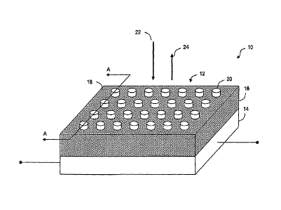
An exemplary embodiment of a wavelength selective surface 10 is shown in
FIG. 1. The wavelength selective surface 10 includes at least three
distinguishable layers.
The first layer is an electrically conductive outer or surface layer 12
including an
arrangement of surface elements 20. The surface elements 20 of the outer layer
12 are
disposed at a height above an inner layer including a continuous electrically
conductive
sheet, or ground layer 14. The arrangement of surface elements 20 and ground
layer 14 is
separated by an intermediate layer 16 disposed therebetween. At least one
function of the
intermediate layer 16 is to maintain a physical separation between the
arrangement of
surface elements 20 and the ground layer 14. The intermediate layer 16 also
provides
electrical isolation between the two electrically conductive layers 12, 14.
In operation, wavelength selective surface 10 is exposed to incident
electromagnetic radiation 22. A variable portion of the incident radiation 22
is coupled to
the wavelength selective surface 10. The level of coupling depends at least in
part upon
the wavelength of the incident radiation 22 and a resonant wavelength of the
wavelength
selective surface 10, as determined by related design parameters. Radiation
coupled to
the wavelength selective surface 10 can also be referred to as absorbed
radiation. At
-5-
CA 02633295 2008-06-12
WO 2007/070540
PCT/US2006/047450
other non-resonant wavelengths, a substantial portion of the incident
radiation is reflected
24.
In more detail, the electrically conductive surface layer 12 includes multiple
discrete surface features, such as the electrically conductive surface
elements 20 arranged
in a pattern along a surface 18 of the intermediate layer 16. The discrete
nature of the
arrangement of surface features 20 requires that individual surface elements
20 are
isolated from each other. This also precludes interconnection of two or more
individual
surface elements 20 by electrically conducting paths. Two or more individual
surface
elements which are connected electrically form a composite surface element
which gives
lo rise to a new resonance.
= The electrically conductive surface layer 12 including an arrangement of
surface
elements 20 is typica.11y flat, having a smallest dimension, height, measured
perpendicular
to the intermediate layer surface 18. In general, each surface element 20
defines a surface
shape and a height or thickness measured perpendicular to the intermediate
layer surface
18. In general, the surface shape can be any closed shape, such as closed
curves, regular
polygons, irregular polygons, star-shapes having three or more legs, and other
closed
structures bounded by piecewise continuous surfaces including one or more
curves and
lines. In some embodiments, the surface shapes can include annular features,
such as ring
shaped patch with an open center region. More generally, the annular features
have an
outer perimeter defining the outer shape of the patch and an inner perimeter
defining the
shape of the open inner region of the patch. Each of the outer an inner
perimeters can
have a similar shape, as in the ring structure, or a different shape. Shapes
of the inner and
outer perimeters can include any of the closed shapes listed above (e.g., a
round patch
with a square open center).
The shapes can be selected to provide a resonant response having a preferred
polarization. For example, surface features having an elongated shape provide
a resonant
response that is more pronounced in a polarization that is related to the
orientation of the
elongated shape. Thus, an array of vertically aligned narrow rectangles
produces a
response having a ve:rtically aligned linear polarization. In general,
preferred
polarizations can be linear, elliptical, and circular.
Each of the electrically conductive surface elements 20 is formed with an
electrically conductive material. Such conductive materials include ordinary
metallic
conductors, such as aluminum, copper, gold, silver, platinum, manganese, iron,
nickel,
-6-
CA 02633295 2008-06-12
WO 2007/070540 PCT/US2006/047450
tin, lead, and zinc; as well as combinations of one or more metals in the form
of a metallic
alloy, such as steel, and ceramic conductors such as indium tin oxide and
titanium nitride.
Alternatively or in addition, conductive materials used in formation of the
surface
elements 20 include semiconductors. Preferably, the semiconductors are
electrically
conductive. Exemplary semiconductor materials include: silicon and germanium;
compound semiconductors such as silicon carbide, gallium-arsenide and indium-
phosphide; and alloys such as silicon-germanium and aluminum-gallium-arsenide.
Electrically conductive semiconductors are typically doped with one or more
impurities
in order to provide good electrical conductivity. Similarly, the ground layer
14 can
io include one or more electrically conductive materials, such as those
described herein.
The intermediate layer 16 can be formed from an electrically insulative
material,
such as a dielectric providing electrical isolation between the arrangement of
surface
elements 20 and the wound layer 14. Some examples of dielectric materials
include
silicon dioxide (Si02); alumina (A1203); aluminum oxynitride; silicon nitride
(Si3N4).
Other exemplary dielectrics include polymers, rubbers, silicone rubbers,
cellulose
materials, ceramics, glass, and crystals. Dielectric materials also include:
semiconductors, such as silicon and germanium; compound semiconductors such as
silicon carbide, gallium-arsenide and indium-phosphide; and alloys such as
silicon-
germanium and aluminum-gallium-arsenide; and combinations thereof. As
dielectric
materials tend to concentrate an electric field within themselves, an
intermediate
dielectric layer 16 will do the same, concentrating an induced electric field
between each
of the surface elements 20 and a proximal region of the wound layer 14.
Beneficially,
such concentration of the electric-field tends to enhance electromagnetic
coupling of the
arrangement of surface elements 12 to the ground layer 14.
Dielectric materials can be characterized by parameters indicative of their
physical
properties, such as the real and imaginary portions of the index of
refraction, often
referred to as "n" and "k." Although constant values of these parameters n, k
can be used
to obtain an estimate of the material's performance, these parameters are
typically
wavelength dependent for physically realizable materials. In some embodiments,
the
intermediate layer 16 includes a so-called high-k material. Examples of such
materials
include oxides, which can have k values ranging from 0.001 up to 10.
The arrangement of surface elements 20 can be configured in a preferred
arrangement, or array on the intermediate layer surface 18. Referring now to
FIG. 2, the
-7-
CA 02633295 2008-06-12
WO 2007/070540
PCT/US2006/047450
wavelength selective surface 10 includes an exemplary array of flattened,
electrically
conductive surface elements 20. Multiple surface elements 20 are arranged in a
square
grid along the intermediate layer surface 18. A square grid or matrix
arrangement is an
example of a regular array, meaning that spacing between adjacent surface
elements 20 is
substantially uniform. Other examples of regular arrays, or grids include
hexagonal grids,
triangular grids, oblique grids, centered rectangular grids, and Archimedean
grids. In
some embodiments, the arrays can be irregular and even random. Each of the
individual
elements 20 can have substantially the same shape, such as the circular shape
shown.
Although flattened elements are shown and described, other shapes are
possible.
to For example, each of the multiple surface elements 20 can have non-flat
profile with
respect to the intermediate layer surface 18, such as a parallelepiped, a
cube, a dome, a
pyramid, a trapezoid, or more generally any other shape. One major advantage
of the
present invention over other prior art surfaces is a relaxation of the
fabrication tolerances.
The high field region resides underneath each of the multiple surface elements
20,
between the surface clement 20 and a corresponding region of the ground layer
14.
In more detail, each of the circular elements 20 has a respective diameter D.
In
the exemplary square grid, each of the circular elements 20 is separated from
its four
immediately adjacent. surface elements 20 by a uniform grid spacing A measured
center-
to-center. An alternative embodiment of another wavelength selective surface
40
= 20 including a hexagonal arrangement, or array of surface elements 42 is
shown in FIG. 3.
Each of the discrete surface elements includes a square surface element 44
having a side
dimension 13'. Center-to-center spacing between immediately adjacent elements
44 of the
hexagonal array 42 is about A'. For operation in the infrared portion of the
electromagnetic spectrum, D will generally be between about 0.5 microns for
near
infrared and 50 microns for the far infrared and terahertz, understanding that
any such
limits are not firm and will very depending upon such factors as n, k, and the
thickness of
layers.
Array spacing A can be as small as desired, as long as the surface elements 20
do
not touch each other. Thus, a minimum spacing will depend to some extent on
the
dimensions of the surface feature 20. Namely, the minimum spacing must be
greater than
the largest diameter of the surface elements (i.e., A > D). The surface
elements can be
separated as far as desired, although absorption response suffers from
increased grid
spacing as the fraction of the total surface covered by surface elements falls
below 10%.
-8-
CA 02633295 2008-06-12
WO 2007/070540 PCT/US2006/047450
=
In some embodiments, more than one arrangement of uniform-sized features are
provided along the same outer surface layer of a wavelength selective surface.
Shown in
FIG. 4 is a plan view of one such device 100 having two different arrangements
of
electrically conductive features 102a, 102b (generally 102) disposed along the
same
surface. The first arrangement 102a includes a triangular array, or grid, of
uniform-sized
circular patches 104a, each having a diameter Di and separated from its
nearest neighbors
by a uniform grid spacing A. Similarly, the second arrangement 102b includes a
triangular grid of uniform-sized circular patches 104b, each having a diameter
D2 and
separated from its nearest neighbors by a uniform grid spacing A. Visible
between the s
circular patches 104a, 104b is an outer surface 18 of the intermediate layer.
Each of the
arrangements 102a, 102b occupies a respective, non-overlapping region 106a,
106b of the
intermediate layer surface 18. Except for there being two different
arrangements 102a,
102b on the same surface 18, the device 100 is substantially similar to the
other
wavelength selective devices described hereinabove. That is, the device 100
also includes
a ground plane 14 (not visible in this view) and an intermediate insulating
layer 16
disposed between the ground plane 14 and a bottom surface of the circular
patches 104a,
104b.
Continuing uith this illustrative example, each of the different arrangements
102a,
102b is distinguished from the other by the respective diameters of the
different circular
patches 104a, 104b (i.e., D2 > Di). Other design attributes including the
shape (i.e.,
circular), the grid format (i.e., triangular), and the grid spacing of the two
arrangements
102a, 102b are the substantially the same. Other variations of a
multilresonant device are
possible with two or more different surface arrangements that differ from each
other.
according to one or. more of: shape; size; grid format; spacing; and choice of
materials.
Size includes thickness of each of the multiple layers 14, 16, 102 of the
device 100.
Different materials can also be used in one or more of the regions 106a, 106b.
For
example, an arrangement of gold circular patches 102a in one region 106a and
an
arrangement of aluminum circular patches 102b in another region 106b.
In operation, each of the different regions 106a, 106b will respectively
contribute
to a different resonance from the same wavelength selective device 100. Thus,
one
device can be configured to selectively provide a resonant response to
incident
electromagnetic radiation within more than one spectral regions. Such features
are .
beneficial in IR applications in which the device 100 provides resonant
emission peaks in
-9-
CA 02633295 2008-06-12
WO 2007/070540 PCT/US2006/047450
more than one IR band. Thus, a first resonant peak can be provided within a 3-
5 pm IR
band, while a second resonant peak can be simultaneously provided within a 7-
14 pm IR
band, enabling the same device to be simultaneously visible to IR detectors
operating in
either of the two IR bands.
In some embodiments, the different arrangements 102a' and 102b' can overlap
within at least a portion of the same region. An exemplary embodiment is shown
in
FIG. 5 having a substantially complete overlap, in which a first arrangement
102a'
includes a triangular grid of uniform-sized circular patches 104a' of a first
diameter Di,
interposed within the same region with a second arrangement 102b' including a
triangular
grid of uniform-sized. circular patches 104b' of a second diameter D2. Each
arrangement
102a', 102b' has a grid spacing of A. When exposed to incident electromagnetic
radiation, device 100' will produce more than one resonant features, with each
resonant
feature corresponding to a respective one of the different arrangements 102a',
102b'. As
with the previous example, one or more of the parameters including: shape;
size; grid
format; spacing; and choice of materials can be varied between the different
arrangements
102a', 102b'.
In yet other embodiments (not shown), devices similar to those described above
in
relation to FIG. 4 and FIG. 5 are formed having a complementary surface. Thus,
a single
device includes two or more different arrangements of through holes formed in
an
electrically conductive layer above and isolated from a common ground layer.
One or
more of the through-hole size, shape, grid format, grid spacing, thickness,
and materials
can be varied to distinguish the two or more different arrangements. Once
again, the
resulting device exhibits at least one respective resonant feature for each of
the two or
more different arrangements.
An exemplary embodiment of an alternative family of wavelength selective
surfaces 30 is shown in FIG. 6. The alternative wavelength selective surfaces
30 also
include an intermediate layer 16 stacked above a ground layer 14; however, an
electrically conductive surface 32 layer includes a complementary feature 34.
The
complementary feature 34 includes the electrically conductive layer 32
defining an
arrangement of through apertures, holes, or perforations.
The electrically conductive layer 32 is generally formed having a uniform
thickness. The arrangement of through apertures 34 includes multiple
individual through
apertures 36, each exposing a respective surface region 38 of the intermediate
layer 16.
-10-
.
CA 02633295 2008-06-12
WO 2007/070540 PCT/US2006/047450
Each of the through apertures 36 forms a respective shape bounded by a closed
perimeter
formed within the conductive layer 32. Shapes of each through aperture 36
include any
of the shapes described above in reference to the electrically conductive
surface elements
20 (FIG. I), 44 (FIG. 3).
Additionally, the through apertures 36 can be arranged according to any of the
configurations described above in reference to the electrically conductive
surface
elements 20, 44. This includes a square grid, a rectangular grid, an oblique
grid, a
centered rectangular grid, a triangular grid, a hexagonal grid, and random
grids. Thus,
any of the possible arrangements of surface elements 36 and corresponding
exposed
regions of the intermediate layer surface 18 can be duplicated in a
complementary sense
in that the surface elements 20 are replaced by through apertures 36 and the
exposed
regions of the intermediate layer surface 18 are replaced by the electrically
conductive
layer 32.
A cross-sectional elevation view of the wavelength selective surface 10 is
shown
in FIG. 7A. The electrically conductive ground layer 14 has a substantially
uniform
thickness HG. The intermediate layer 16 has a substantially uniform thickness
HD, and
each of the individual surface elements 20 has a substantially uniform
thickness H. The
different layers 12, 1.4, 16 can be stacked without gaps therebetween, such
that a total
thickness HT of the resulting wavelength selective surface 10 is substantially
equivalent to
the sum of the thicknesses of each of the three individual layers 14, 16, 12
(i.e., HT = HG
+ HD + Hp). A cross-sectional elevation view of the complementary wavelength
selective
surface 30 is shown in FIG. 7B and including a similar arrangement of the
three layers 14,
16, 32.
In some embodiments, the intermediate insulating layer has a non-uniform
thickness with respect to the ground layer. For example, the intermediate
layer may have
a first thickness HD under each of the discrete conducting surface elements
and a different
thickness, or height at regions not covered by the surface elements. It is
important that a
sufficient layer of insulating material be provided under each of the surface
elements to
maintain a design separation and to provide isolation between the surface
elements and
the ground layer. In at least one example, the insulating material can be
substantially
removed at all regions except those immediately underneath the surface
elements. In
other embodiments, the insulating layer can include variations, such as a
taper between '
-11-
CA 02633295 2008-06-12
WO 2007/070540 PCT/US2006/047450
surface elements. At least one benefit of the inventive design is a relaxation
of design
tolerances that results in a simplification of fabrication of the devices.
The thickness chosen for each of the respective layers 12, 32, 16, 14 (HP) HD,
HG)
can be independently varied for various embodiments of the wavelength
selective
surfaces 10, 30. For example, the ground plane 14 can be formed relatively
thick and
rigid to provide a support structure for the intermediate and surface layers
16, 12, 32.
Alternatively, the ground plane 14 can be formed as a thin layer, as long as a
thin ground
plane 14 forms a substantially continuous electrically conducting layer of
material
providing the continuous ground. Preferably, the round plane 14 is at least as
thick as one
lo skin depth within the spectral region of interest. Similarly, in
different embodiments of
the wavelength selective surfaces 10, 30, the respective surface layer 12, 32
can be
formed with a thickness Hp ranging from relatively thin to relatively thick.
In a relatively
thin embodiment, the surface layer thickness Hp can be a minimum thickness
required
just to render the intermediate layer surface 18 opaque. Preferably, the
surface layer 12,
32 is at least as thick as one skin depth within the spectral region of
interest.
Likewise, the intermediate layer thickness HD can be formed as thin as
desired, as
long as electrical isolation is maintained between the outer and inner
electrically
conducting layers 12, 32, 14. The minimum thickness can also be determined to
prevent
electrical arcing between the isolated conducting layers under the highest
anticipated
induced electric fields. Alternatively, the intermediate layer thickness HD
can be formed
relatively thick. The concept of thickness can be defined relative to an
electromagnetic
wavelength `2+,c' of operation, or resonance wavelength. For example, the
intermediate
layer thickness HD can be selected between about 0.01A.c in a relatively thin
embodiment
to about 0.52c in a relatively thick embodiment.
Referring to FIG. 7C, a cross sectional view of a wavelength selective device
38
includes an arrangement of surface features 20 disposed over ground plane 14,
with an
intermediate insulating layer 16 disposed between the surface features 20 and
the ground
plane 14. The device 38 also includes a second intermediate layer 39 disposed
between a
top surface 18 of the insulating layer and a bottom surface of the surface
features 20. The
second layer 39 is also an insulating material, such that the individual
surface features 20
remain discrete and electrically isolated from each other with respect to a
non time-
varying electrical stimulus. For example, the second intermediate layer 39 can
be formed
from a dielectric material chosen to have material properties n, k different
than the
-12-
CA 02633295 2008-06-12
WO 2007/070540 PCT/US2006/047450
material properties of the first intermediate layer 16. Any dielectric
material can be used
including any of the dielectric materials described herein. Alternatively or
in addition,
the second intermediate layer 39 can be formed from a semiconductor material.
Any
semiconductor can be used, including those semiconductor and semiconductor
compounds described herein, provided that the semiconductor includes an
electrically
insulating mode. More generally, a fourth layer having physical properties
described
above in relation to the second intermediate layer 39 can be provided between
any of the
three layers 14, 16, 20 of the device 38.
The wavelength selective surfaces 10, 30 can be formed using standard
semiconductor fabrication techniques. Thin devices can be obtained using
standard
fabrication techniques on a typical semiconductor substrate, followed by a
release step,
which the thin device is released from the substrate. One such technique is
referred to as
back-side etching, in which a sacrificial layer is removed underneath the
device formed
upon the semiconductor substrate. Removal of the sacrificial layer releases a
thin-film
device from the substrate.
Alternatively or in addition, the wavelength selective surfaces 10, 30 can be
formed using thin film techniques including vacuum deposition, chemical vapor
deposition, and sputtering. In some embodiments, the conductive surface layer
12,44 can
be formed using printing techniques. The surface features can be formed by
providing a
continuous electrically conductive surface layer and then removing regions of
the surface
layer to form the surface features. Regions can be formed using standard
physical or
chemical etching techniques. Alternatively or in addition, the surface
features can be
formed by laser ablation, removing selected regions of the conductive material
from the
surface, or by nano-imprinting.or stamping, or other fabrication methods known
to those
skilled in the art.
Referring to FIG. 8A a cross-sectional elevation view of an alternative
embodiment of a wavelength selective surface 50 is shown having an over layer
52.
Similar to the embodiments described above, the wavelength selective surface
50 includes
an electrically conductive outer layer 12 having an arrangement of surface
elements 20
(FIG. 1) disposed at a height above a ground layer 14 and separated therefrom
by an
intermediate layer 16. The over layer 52 represents a fourth layer, or
superstrate 52
provided on top of the electrically conductive surface layer 12.
-13-
CA 02633295 2008-06-12
WO 2007/070540
PCT/US2006/047450
The over layer 52 can be formed having a thickness FIc I measured from the
intermediate layer surface 18. In some embodiments, the over layer thickness
Hci is
greater than thickness of the surface elements 20 (i.e., Hci > Hp). The over
layer 52 can
be formed with varying thickness to provide a planar external surface.
Alternatively or in
addition, the over layer 52 can be formed with a uniform thickness, following
a contour
of the underlying electrically conductive surface 12.
An over layering material 52 can be chosen to have selected physical
properties
(e.g., k, n) that allow at least a portion of incident electromagnetic
radiation to penetrate
into the over layer 52 and react with one or more of the layers 12, 14, and 16
below. In
some embodiments, the overlying material 52 is optically transparent in the
vicinity of the
primary absorption wavelength, to pass substantially all of the incident
electromagnetic
radiation. For example, the overlying material 52 can be formed from a glass,
a ceramic,
a polymer, or a semiconductor. The overlaying material 52 can be applied using
any one
or more of the fabrication techniques described above in relation to the other
layers 12,
14, 16 in addition to painting and/or dipping.
In some embodiments, the over layer 52 provides a physical property chosen to
enhance performance of the wavelength selective device in an intended
application. For
example, the overlaying material 52 may have one or more optical properties,
such as
absorption, refraction, and reflection. These properties can be used to
advantageously
modify incident electromagnetic radiation. Such modifications include
focusing, de-
focusing, and filtering. Filters can include low-pass, high-pass, band pass,
and band stop.
The overlaying material 52 can be protective in nature allowing the wavelength
selective surface 50 ID function, while providing environmental protection.
For example,
the overlaying material 52 can protect the surface conductive layer 12 from
corrosion and
oxidation due to exposure to moisture. Alternatively or in addition, the
overlaying
material 52 can protect either of the exposed layers 12, 16 from erosion due
to a harsh
(e.g., caustic) enviro:runent. Such harsh environments might be encountered
routinely
when the wavelength selective surface is used in certain applications. At
least one such
application that would benefit from a protective overlaying material 52 would
be a marine
application, in which a protective over layer 52 would protect the
electrically conductive
layer 12 or 32 from corrosion.
In another embodiment shown in FIG. 8B, a wavelength selective surface 60 =
includes an overlying material 62 applied over a conductive layer 32 defining
an
-14-
CA 02633295 2008-06-12
WO 2007/070540 PCT/US2006/047450
arrangement of through apertures 34 (FIG. 6). The overlying material 62 can be
applied
with a maximum thickness Hc2 measured from the intermediate layer surface 18
to be
greater than the thickness of the conductive layer 32 (i.e., H2> Hp). The
overlaying
material 62 again can provide a planar external surface or a contour surface.
Accordingly, a wavelength selective surface 60 having apertures 34 defined in
an
electrically conductive layer 32 is covered by an overlying material 62. The
performance
and benefits of such a device are similar to those described above in relation
to FIG. 8A.
Referring to FIG. 9A, an exemplary reflectivity versus wavelength response
curve
70 of a representative narrow-resonance response is shown in graphical form.
The
io response curve 70 is achieved by exposing a wavelength selective surface
10 (FIG. 1)
constructed in accordance with the principles of the present invention to
incident
electromagnetic radiation 22 (FIG. 1) within a band including a resonance. As
shown, the
reflectivity to incident electromagnetic radiation varies according to the
curve 70 within
the range of 0% to 100%. As the wavelength of the incident radiation 22 is
varied from 2
to 20 microns, the reflectivity starts at a relatively high value of about
75%, increases to a
value of over 85% at about 3 microns, reduces back to about 75% at about 3.5
microns,
and increases again to nearly 100% between about 3.5 and 7 microns. Between 7
and 8
microns, the reflectivity response curve 70 incurs a second and more
pronounced dip 72
to less then 20% reflectivity. The second dip 72 is steep and narrow,
corresponding to
absorption of incident electromagnetic radiation by the surface 10. The
reflectivity
response curve 70 at wavelengths beyond about 8 microns rises sharply back to
more than
90% and remains above about 80% out to at least 20 microns. This range, from 2
to 20
microns, represents a portion of the electromagnetic spectrum including
infrared
radiation.
The second and much more pronounced dip 72 corresponds to a primary
resonance of the underlying wavelength selective surface 10. As a result of
this
resonance, a substantial portion of the incident electromagnetic energy 22 is
absorbed by
the wavelength selective surface 10. A measure of the spectral width of the
resonance
response 70 can be determined as a width in terms of wavelength normalized to
the
resonant wavelength (i.e., AX/Xe or d2J2t.c). Preferably, this width is
determined at full- -
width-half-maximum (FWHM). For the exemplary curve, the width of the
absorption
band at FWHM is less than about 0.2 microns with an associated resonance
frequency of
about 7 microns. This results in a spectral width, or dX/X.c of about 0.03.
Generally, a
-15-
CA 02633295 2008-06-12
WO 2007/070540 PCT/US2006/047450
dX/21/4õ value of less than about 0.1 can be referred to as narrowband. Thus,
the exemplary
resonance is representative of a narrowband absorption response.
Results supported by both computational analysis of modeled structures and
measurements suggest that the resonant wavelength associated with the primary
resonance response 7:2 corresponds to a maximum dimension of the electrically
conductive surface elements (e.g., a diameter of a circular patch D, or a side
length of a
square patch D'). As the diameter of the surface elements is increased, the
wavelength of
the primary absorption band 72 also increases. Conversely, as the diameter of
the surface
elements is decreased, the wavelength of the primary absorption band 72 also
decreases.
The first, less pronounced dip 74 in reflectivity corresponds to a secondary
absorption band of the underlying wavelength selective surface 10. Results
supported by
both computational analysis of modeled structures and measurements suggest
that the
wavelength associated with the secondary absorption band 74 corresponds at
least in part
to a center-to-center spacing of the multiple electrically conductive surface
elements. As
the spacing between surface elements 20 in the arrangement of surface elements
12 is
reduced, the wavelength of the secondary absorption band 74 decreases.
Conversely, as
the spacing between the arrangement of surface elements 12 is increased, the
wavelength
of the secondary absorption band 74 increases. The secondary absorption band
74 is
typically less pronounced than the primary absorption band 72, such that a
change in
reflectivity AR can be determined between the two absorption bands 74,72. A
difference
in wavelength between the primary and secondary absorption bands 72, 74 is
shown as
AVV.
In general, the performance may be scaled to different wavelengths according
to
the desired wavelength range of operation. Thus, by scaling the design
parameters of any
of the wavelength selective surfaces as described herein, resonant performance
can be
obtained within any desired region of the electromagnetic spectrum. Resonant
wavelengths can range down to visible light and even beyond into the
ultraviolet and X-
ray. At the other end of the spectrum, the resonant wavelengths can range into
the
terahertz band (e.g., wavelengths between about 1 millimeter and 100 microns)
and even
up to radio frequency bands (e.g., wavelengths on the order of centimeters to
meters).
Operation at the shortest wavelengths will be limited by available fabrication
techniques.
Current techniques can easily achieve surface feature dimensions to the sub-
micron level.
It is conceivable that such surface features could be provided at the
molecular level using
-16-
CA 02633295 2008-06-12
WO 2007/070540 PCT/US2006/047450
currently available and emerging nanotechnologies. Examples of such techniques
are
readily found within the field of micro-mechanical-electrical systems (MEMS).
An exemplary reflectivity versus wavelength response curve 110 is shown in
FIG.
9B for a device 100 (FIG. 4) having more than one primary resonances. In this
example,
a first resonance 112a occurs at about 4.5 pm and a second resonance 112b
occurs at
about 9 pm. Also identified on the graph are two different channels within the
IR band.
A first channel 114a extends from about 3 pm to about 5 pm; whereas, the
second
channel 114b extends from about 7 pm to about 14 JAM. Advantageously, the
first
resonance 112a resides within the first IR channel 114a and the second
resonance 112b
io resides within the second IR channel 114b. In other embodiments of the
present
invention, one or more of the resonances 112a, 112b can be selected through
the proper
choice of design parameters, to reside at a wavelength outside of a channel
114a, 114b.
Referring to FIG. 9C, an exemplary reflectivity versus wavelength response
curve
80 of a wide-resonance wavelength selective surface is shown in graphical
form. This
wideband response curve 80 can also be achieved with the wavelength selective
surface
10 (FIG. 1) constructed in accordance with the principles of the present
invention, but
having a different selection of design parameters. Here, a primary absorption
band 82
occurs at about 8 microns, with wavelength range at FWHM of about 3 microns.
This
results in a spectral width AX/X. of about 0.4. A spectral width value AVX,
greater than
zo 0.1 can be referred to as broadband. Thus, the underlying wavelength
selective surface
10 can also be referred to as a broadband structure.
One or more of the physical parameters of the wavelength selective surface 10
can
be varied to control reflectivity and absorption-emission response of a given
wavelength
selective surface. For example, the thickness of one or more layers (e.g.,
surface element
thickness Hp, dielectric layer thickness HD, and over layer thickness HO can
be varied.
Alternatively or in addition, one or more of the materials of each of the
different layers
can be varied. For example, the dielectric material can be substituted with
another
dielectric material having a different n and k values. The presence or absence
of an over
layer 52 (FIG. 8A), as well as the particular material selected for the over
layer 52 can
also be used to vary the reflectivity or absorption-emission response of the
wavelength
selective surface. Similar performance changes may be achieved by changing the
material of the ground plane, change the dimension D of the surface elements,
or by
changing the shape of the surface elements.
-17-
CA 02633295 2008-06-12
WO 2007/070540 PCT/US2006/047450
In a first example, a wavelength selective surface includes an intermediate
layer
formed with various diameters of surface patches. The wavelength selective
surface
includes a triangular array of round aluminum patches placed over an aluminum
film
ground layer. The various surfaces are each formed with surface patches having
a
s different respective diameter. A summary of results obtained for the
different patch
diameters is included in Table 1. In each of these exemplary embodiments, the
patch
spacing between adjacent patch elements was about 3.4 microns, and the
thickness or
depth of the individual patches and of the ground layer film were each about
0.1 micron.
An intermediate, dielectric layer having thickness of about 0.2 microns was
included
between the two aluminum layers. It is worth noting that the overall thickness
of the
wavelength selective surface is about 0.4 microns ¨ a very thin material. The
exemplary
dielectric has an index of refraction of about 3.4. Table 1 includes
wavelength values
associated with the resulting primary absorptions. As shown, the resonant
wavelength
increases with increasing patch size.
Table 1. Primary Absorption Wavelength Versus Patch Diameter
Patch Diameter Resonant Wavelength (Xe)
1.25 f1111 4.1 gm
1.75 1.mi 5.5 p.m
______________________ 2.38 pm 7.5 gm
______________________ 2.98 pm 9.5 gm
In another example, triangular arrays of circular patches having a uniform
array
spacing of 3.41nicro.as and patch diameter of 1.7 microns are used. A
dielectric material
provided between the outer conducting layers is varied. As a result, the
wavelength of the
primary absorption shifts. Results are included in Table 2.
Table 2. Resonance Versus Dielectric Material
¨ Dielectric material Resonant Wavelength (Xc)
Oxide 5.8 pm
Nitride 6.8 pm
Silicon 7.8 pm
Referring to FIG. 10, an exemplary emissivity versus wavelength curve 120a is
shown within a porti:on of the IR spectrum for a device fabricated in
accordance with the
-18-
CA 02633295 2014-03-12
present invention. When combined with a thermal source of radiation,
wavelength
selective surfaces according to the principles of the present invention
produce a resonant
response in emissivity as determined at least in part to one or more physical
aspects of the
underlying device.
As shown, the emissivity 120a is relatively low (e.g., below about 0.04) for
wavelengths both below about 4 pm and above about 6 p.m. However, at
wavelengths
between 4 pm and 6 i.tm a sharp rise in emissivity occurs producing a peak
emissivity
122a corresponding to a resonant wavelength of the device. In the exemplary
figure, the
peak emissivity 122a is about 0,15 at a corresponding resonant frequency of
about
4.5 pm. As with reflectivity, a measure of the resonant response can be
defined by its
selectivity determined as the spectral width at FWHM divided by the resonant
frequency
(i.e., &c/?.c). A selectivity value of the first resonant peak is about 0.1,
for narrowband
operation.
Also shown is a second curve 120b having a different emissivity of about 0.06
at
about 7.5 pm. Superimposed is a representative black body curve 124. Variation
of one
or more of the design parameters as described herein can be used to choose the
resonant
wavelength 122a, 122b. Thus, when the wavelength selective device or surface
producing either curve I20a, 120b is applied to a thermal source, such as a
filamentary
heater, the emissivity of the blackbody thermal source is modified
substantially to radiate
only within a narrow band of wavelengths corresponding to resonance frequency.
Thus, a
narrowband (i.e., AA,ent,c < 0.1) thermal source is possible combining the
wavelength
selective device with a broadband thermal radiation source to produce a
substantially
coherent IR source.
At least one important application for wavelength selective devices according
to
principles of the present invention is in gas detectors. As described in U.S.
Patent No.
7,119,337, a narrowband
thermal source
can be tuned to an absorption band of a target gas. A sample of a substance,
such as a gas
is illuminated with the narrowband thermal source. A portion of the emitted
spectrum is
detected after propagating through the sample. When the target gas is present,
the
detected radiation will be substantially less due to absorption by the gas.
Referring to FIG. 11, a thermal source 130 includes a narrowband IR source 132
within an electrical device package 134. In an exemplary embodiment, the IR
source 132
is a horizontal thin film prepared in accordance with the device of FIG. 1,
including an
-19-
CA 02633295 2008-06-12
WO 2007/070540 PCT/US2006/047450
arrangement of uniform-sized electrically conductive surface patches above a
ground
plane separated by an intermediate thin-film layer of insulating material. The
ground
plane is provided with a finite conductivity having a real resistive
component. The thin
film device 132 is suspended in a bridge configuration between a pair of
vertical support
members 134a, 134b. Electrical terminals 136a, 136b are used to inject an
electrical
current into the ground plane of the emission device 132 to produce thermal
energy
through a process referred to as Joule heating, or equivalently as I2R
heating.
The device package 133 may include a sealed housing, such as a TO-8 transistor
used in standard process equipment, to isolate the IR source 132 from the
environment.
The package 133 includes at least one window 138 substantially aligned with an
emission
surface of the IR source 132, such that IR emissions can exit the package 133
to interact
with the environment. The window 138 may include one or more optical
properties
including reflection, absorption, and transmission. In some embodiments, the
device 130
includes a feature, such as the collar 135 shown providing a smooth reflective
surface
disposed around the fIt. source 132 and adapted to collect radiation emitted
from the
surface to selectively direct IR emissions within a preferred direction.
Alternatively or in
addition, a reflective member 133 is provided on the floor of the package,
underneath the
suspended IR source 132 (e.g., on an interior surface of the header of the
transistor can
shown) to reflect emission from a back side of the IR source 132 toward the
window 138.
Additionally, the package 133 includes one or more electrical leads 139a, 139b
that can
be used to inject an electrical current to drive the IR source 132. More
generally, the IR
source 132 includes any of the thin film wavelength selective surfaces
described herein
combined with a thin film thermal source ¨ which can be the ground plane.
In some embodiments, a wavelength selective device, such as the IR source 132
above, includes additional layers, including a different respective insulating
layer on each
surface of the ground layer. Each insulating layer can have a respective
arrangement of
electrically conductive surface elements. Such a device is bidirectional in
that it provides
a respective reflectivity-absorption and emission profile on either side of
the ground
plane. A resonant performance of each of the different sides is independently
controllable
according to selected design parameters. In some embodiments, the design
parameters of
each side of the device are substantially identical yielding similar
resonances.
Alternatively, the design parameters of each side of the device are
substantially different
yielding different resonances.
-20-
CA 02633295 2008-06-12
WO 2007/070540 PCT/US2006/047450
Referring to FIG. 12, an IR source 140 can include a first IR source 142a
formed
in a ribbon or filament configuration. The first filament 142a can be formed
in a
serpentine shape, as shown, having electrical terminals 144a, 144b at either
end. The
electrical current can be applied between the terminals 144a, 144b causing a
resistive
ground plane to heat.
A second filament 142b can be provided within the same IR source 140.
Preferably, the second filament 142b is constructed similar to the first 142a.
In some
embodiments, the second filament 142b is used as a detector, detecting a
reflected return
of IR emissions from the first filament 142a. In some embodiments, the second
filament
142b is covered, or "blinded" by a screen 146. Thus, the second filament 142
shielded by
the screen 146 does not respond to received IR from outside the package, but
is allowed
to respond to other environmental and device-dependent effects, such as
ambient
temperature and long-term variations in performance due to aging of the
device. When
formulated from the same material, the second filament 142b can be used as a
reference
to compare response measured on the first filament 142a. Thus, effects due to
ambient
temperature and long-term aging can be effectively removed from measurements
obtained
from the first.
In general, drive and readout schemes using a microprocessor controlled,
temperature-stabilized driver can be used to determine resistance from drive
current and
zo drive voltage readings. That information shows that incidental
resistance (temperature
coefficient in leads and packages and shunt resistors, for instance) do not
overwhelm the
small resistance changes used as a measurement parameter.
For embodiments using a second detector for reference, the devices can be
configured in a balanced bridge. Referring to FIG. 13, a Wheatstone bridge
drive circuit
160 is shown. The Wheatstone bridge is a straightforward analog control
circuit used to
perform the function of measuring small resistance changes in a detector. It
is very
simple, very accurate, quite insensitive to power supply variations and
relatively
insensitive to temperature. The circuit is "resistor" programmable but depends
for
stability on matching the ratio of resistors. In one form, an adjacent "blind"
detector
element ¨ an identical bolometer element filtered at some different waveband ¨
is used as
the resistor in the other leg of the bridge,.allowing compensation for
instrument and
component temperatures and providing only a difference signal related to
infrared
absorption in the target gas.
-21-
CA 02633295 2008-06-12
WO 2007/070540 PCT/US2006/047450
In some embodiments, a wavelength selective emission device can be operated as
both a source and a detector. For example, the emission device is heated using
a thermal
source, such as a resistive filament excited by an electrical current. The
infrared radiation
excites the arrangement of surface elements establishing a resonant coupling
of the
s surface elements to other surface elements and to the ground plane. The
result is an IR
emission having a preferred spectra width (e.g., narrowband or wideband,
depending
upon the selection of design parameters). Heat is then removed from the source
and the
emission device is allowed to cool. The device can be used as a bolometer also
detecting
IR from an external environment or its own self-emission. The minimum duration
of
time between heating and cooling is limited by the thermal relaxation of the
emission
device. Preferably the thin film device is extremely thin, on the order of 10
pm or less,
providing a very low thermal mass. Such thin film devices are capable of rapid
cooling
and can support thermal cycles approaching 1 to 2 Hz or even greater.
Referring to FIG. 14A, one embodiment of a target material detector 85
provides
an IR source including wavelength selective emission device 87 as described
herein.
Thus, the emission device 87 emits IR radiation at a wavelength selected to
coincide with
an absorption band of a target material, such as a gas. The resonant emission
device 87 is
aligned to emit radiation toward a target material (e.g., a gas). A reflecting
surface such
as a retro-reflective mirror, or a spherical mirror 84, is positioned opposite
the emission
device 87 (e.g., at a radial center of the spherical mirror), leaving a
channel therebetween
to accommodate a sample of the gas to be inspected for presence of the target
component.
In operation, radiation emitted from the emission device 87 passes through the
gas sample
toward the mirror 84. That portion of emitted radiation not absorbed by the
sample gas
reflects off of the mirror 84 and travels back toward the emission device 87
traversing the
sample gas once again. When configured to act as an absorber and a receiver,
the
emissive device 87 detects the amount of received energy at the resonant
wavelength.
The detected value can be compared to the emitted value to determine an
absorption value
indicative of the target gas.
When a wavelength selective surface having multiple resonances is used, each
of
the multiple resonances can be individually tuned to a respective one of more
than one
target components. Such a device 85 is capable of detecting a preferred
combination of
different target elements. When all of the two or more target elements are
present,
absorption of the mufti-resonant emissions result in a minimum detected
return, as all of
-22-
CA 02633295 2008-06-12
WO 2007/070540 PCT/US2006/047450
the multiple resonant emissions will endure absorption. However, when one or
more of
the two or more target elements are absent from the mixture, at least one of
the
corresponding resonant radiation emissions will suffer little or no absorption
yielding a
non-minimum detected return.
In some embodiments, a second emission device 86 is provided in the vicinity
of
the first 87. The first emission device 87 is tuned to the gas, while the
second emission
device 86 is tuned to a different wavelength, chosen to be outside the
absorption band of
any target elements in the gas. The return from the second emission device 86
can be
used to measure other effects, such as ambient temperature changes and long-
term
changes due to device degradation. Results from the second emission device 86
can be
combined with results from the first device 87, using techniques described
herein, to
effectively remove these secondary effects.
Referring to FIG. 14B, another embodiment of a reflective gas sensor 85' using
a
separate emission device 87' and detection device 86'. A mirror 84' is
disposed within
the optical path between the emission device 87' and the detection device 86'.
The
sample material is also disposed between the optical path, such that emitted
radiation
traverses the sample, such that absorption by a target element will bet
evident by a
reduced return at the detector 86'.
In some embodiments, at least one of the layers of a wavelength selective
device
provides a controllable electrical conductivity. Preferably, the conductivity
of the
associated layer can be controlled using an external control mechanism to
alter the
resonant performance: of the wavelength selective device. Referring now to
FIG. 15A, a
wavelength selective device 200 includes an arrangement of conductive surface
elements
202 disposed above a ground layer 204. The conductive surface elements 202 are
isolated from each other and separated from the ground layer 204 by an
intermediate
insulating layer 206. The wavelength selective device 200 provides a resonant
response
to incident electromagietic radiation that depends on one or more of the
design features
of the device 200 as described herein. In the presence of electromagnetic
radiation at
wavelengths in and around the one or more resonant peaks, electromagnetic
coupling
fields are produced in and around the conductive surface elements 202 and
particularly
within the insulating 'layer 206 between each of the elements 202 and a
localized region
of the ground layer 204.
-23-
CA 02633295 2008-06-12
WO 2007/070540 PCT/US2006/047450
In the exemplary embodiment, an over layer 208 of insulating material covers
the
surface elements 202. In particular, the over layer 208 is made from a
material having an
electrical conductivity value that can be altered by an external control
mechanism. When
controlled to have a first conductivity that is substantially insulating, the
device 200
demonstrates a resonant response to one or more of reflectivity, absorption,
and
emissivity. The first conductivity can be said to provide a relatively high
impedance
value that sufficiently maintains electrical isolation of the conductive
surface elements
202. Upon activation by the external control mechanism, the over layer 208
provides a
second conductivity value that is non-insulating, or electrically conducting.
Being
electrically conductive, or having a relatively low impedance value, the over
layer 208
changes the resonant response of the device 200.
In some embodiments, the over layer 208 includes a semiconductor, such as
silicon. The semiconductor itself behaves as an insulator. When doped with an
appropriate element, the semiconductor can become electrically conductive in
the
presence of an applied electric field. Such techniques are well known to those
skilled in
the art of semiconductor fabrication. In order to provide an electric field to
the
semiconductor material, at least two terminals are provided: a source terminal
210 and a
drain terminal 212. The intermediate insulating layer 206 can include an
oxide, and the
electrically conducting metal ground plane 204 can be used as a gate terminal,
such that
the device represents a metal-oxide-semiconductor (MOS) field effect
transistor (FET).
In particular, the structure represents a form of transistor referred to as a
thin-film
transistor (TFT).
Upon application of a sufficient gate-to-source voltage (Vgs), the electrical
conductivity of the semiconductor over layer 208 changes from insulating (off)
to
conducting (on). Being electrically conducting, the surface elements 202 are
short
circuited together. Such a substantial change to the structure quenches the
electromagnetic fields previously established between the surface elements 202
and the
ground layer 204, thereby change the resonant response. When the surface
elements 202
are shorted together in this manner, the resonant response essentially
disappears, such that
the wavelength selective device 200 can be selectively turned on and off as
desired by
controlling voltage signal applied between the gate and source terminals. This
can be
used to modulate the resonant response, be it reflectivity, absorption, and
emissivity, at
speeds (e.g., kilohertz through megahertz, and higher) much faster than would
otherwise
-24-
CA 02633295 2008-06-12
WO 2007/070540 PCT/US2006/047450
be possible considering the thermal relaxation response of the device. Thus,
the resonant
response is no longer limited by a thermal relaxation between cycles.
In other embodiments, the device 200 includes a similar architecture with an
over
layer 208 formed from an optically responsive material, such as photovoltaic
material.
Without illumination,, or with insufficient illumination below some threshold
value, the
photovoltaic material 208 is substantially insulating allowing the device 200
to exhibit a
resonant response according to the design parameters of the device 200. When
illuminated sufficiently, the conductivity of the over layer 208 changes,
becoming non-
insulating, or electrically conductive. Such an increase in electrical
conductivity
substantially changes the resonant behavior of the device 200 by altering, and
in some
instances, electrically short-circuiting the arrangement surface elements 202.
Thus,
resonant performance of the device at one or more wavelengths of interest can
be
substantially modified by application of light energy at the same or different
wavelengths.
In such an embodiment, there would be no need for either a source terminal 210
or a drain
terminal 212.
Referring to FIG. 15B, a top perspective view of one such device 220 is shown
having an arrangement of surface elements 222 disposed on an insulating
intermediate
layer 224. A ground layer 226 is provided beneath the intermediate layer 224.
An over
layer 227 is applied over the arrangement of surface elements 222, having
source terminal
223 and a drain term:inal 225 disposed along opposite ends of the over layer
227. The
entire device can be formed on a substrate 228. In some embodiments substrate
228 can
be rigid, such as on a base Si wafer providing support to the transistor
structure 220. In
other embodiments, the substrate 228 can be flexible so that the device 220
can be
contoured to the surface on which it is applied. At least one suitable
flexible substrate
includes polyimide films, commercially available from DuPont under the trade
name
KAPTON. Electrical contact can be made from an external source to one or more
of the
gate 226, source 223, and drain 225 terminals, such that application of an
applied
electrical signal can .alter the conductivity of the over layer 227, thereby
changing the
resonant response of the wavelength selective device 220.
More generally, a similar approach can be used to controllably vary the
conductivity of any one of the layers of a multi-layer wavelength selective
device. In one
embodiment, a ground plane layer can be included having a controllable
conductivity. In
some embodiments, the conductivity can be controlled by the application of an
electrical
-25-
CA 02633295 2008-06-12
WO 2007/070540 PCT/US2006/047450
signal. For example, the ground layer can include a suitably doped
semiconductor
material supporting an electrical current in the presence of an electric field
above a
threshold value. Thus, in the presence of a sufficient electric field, the
ground layer
becomes electrically conducting and the wavelength selective device operates
according
to the principals of the invention yielding a resonant response according to
the chosen
design parameters. However, upon variation of the electric field below the
threshold, or
its removal altogether, the ground layer becomes non-conducting, effectively
removing
the ground layer from the device. Such a substantial change in the
configuration of the
device quenches the standing wave electric fields in the dielectric and
changes the overall
reflection or absorption/emission resonance.
In another embodiment, the insulating layer includes a controllable
conductivity.
For example, the conductivity can be controlled by an electrical signal using
a device
such as a semiconductor for the insulating layer. Without application of a
sufficient
controlling electrical field, the insulating layer remains insulating allowing
the
15- wavelength selective device to operate according to the principals of
the present invention
yielding and providing a resonant response according to the chosen design
parameters.
However, upon the application of a sufficient electrical field, the insulating
layer changes
from insulating to non-insulating (or semi-insulating), thereby quenching the
electromagnetic fields in the intermediate layer. Such a substantial change in
the
behavior of the ground layer alters the resonant performance, essentially
turning the
resonant performance off.
In addition to semiconductors, other materials can be used to provide a
electrical
conductivity controllable by an external control signal. Other examples
include
photovoltaic materials as described above and thermally responsive materials,
such as
pyroelectric materials that change conductivity in response to heat. Still
other examples
include chemically responsive materials, such as polymers that change
conductivity in
response to a local chemical environment. For example, the wavelength
selective device
includes an intermediate insulating layer formed from a photoconductor with a
conductivity modified by incident light. Such a device would have an infrared
reflection,
and emission spectrum that could be modified by an external light source.
Alternatively or in addition, the intermediate layer includes a dielectric
layer
having an electrical conductivity that changes in response to its local
chemical and/or
physical environment. Such a device can serve as a remote sensor or tag for
the relevant
-26-
CA 02633295 2008-06-12
WO 2007/070540 PCT/US2006/047450
chemical or physical changes. Such a device can be remotely monitored through
its
infrared reflection/emission signature.
In yet other embodiments, the intermediate dielectric layer can have a
conductivity or index of refraction that can be modified by a combination of
the local
environment and external illumination. One such example includes a fluorescent
polymer.
Any of the above controllable devices can be used as an externally modulated,
tuned electromagnetic emitter. This is particularly advantageous in the
infrared band,
wherein the device can be modulated rapidly, and faster than would otherwise
be possible
in view of thermal relaxation of the material.
A wavelength. selective device that selectively reflects and/or emits
electromagnetic radiation of a preferred wavelength can be used as a picture
element, or
pixel in a display device. Referring to FIG. 16, a pixel 300 is shown
including a two-by-
two rectangular matrix of sub-pixel elements 302a, 302b, 302c, 302d (generally
302). A
pair of column electrodes 304a, 304b (generally 304) is aligned vertically,
with each
column electrode 304 connected to both sub-pixels 203 in its respective
column.
Likewise, a pair of row electrodes 306a, 306b (generally 306) is aligned
horizontally,
with each row electrode 306 connected to both sub-pixels 203 in its respective
row. In
particular, each of the sub-pixels can be individually addressed by applying a
signal to the
singular combination, of column and row electrodes 304, 306 interconnected to
the
addressed sub-pixel 302. The pixel 300 can be formed on a substrate using
techniques
known to those skilled in the art of thin film displays, in which the film
pixel elements
include a resonant reflectivity and/or emissivity response as described
herein.
A schematic representation of a matrix display is shown in FIG. 17, using an
array
of pixel 300 elements according to principles of the present invention. In
some
embodiments, each of the sub-pixels 302 provides a resonant response at a
substantially
equivalent wavelength, or at least within the same band (e.g., the same IR
band). In some
embodiments, the intensity of the reflective response can be varied according
to an
applied control signal of each sub pixel 302. Such variation can be used to
vary the
intensity of a reflectivity dip (absorption spike) without substantially
changing its
resonant wavelength. For emissivity applications, such variation of a control
input can be
used to vary the intensity of emission spike, without substantially changing
its resonant
wavelength. With variations in intensity, the display 310 can be compared to a
black and
-27-
CA 02633295 2008-06-12
WO 2007/070540 PCT/US2006/047450
white visual display, having an array of pixels each displaying a controllable
shade of
gray (i.e., intensity).
In other embodiments, the pixel 300 includes an array of sub-pixels 302 in
which
each sub-pixel is tuned to a different respective wavelength. Thus,
alternatively or in
addition to the ability to control intensity of each of the sub pixels 302 as
described
above, each of the sub-pixels 302 can be actuated to provide a variable
intensity, variable
wavelength response. With variations in intensity and wavelength, the display
310 can be
compared to a color visual display, having an array of pixels each including
an array of
sub-pixels to display different colors and intensity.
Thus, a complex picture can be formed within a portion of the electromagnetic
spectrum determined by the resonant wavelength (e.g., IR), using a matrix
display formed
from a matrix of wavelength selective device as described using the principles
described
herein. The matrix display 310 can operate in a reflection mode, in which the
display 310
is illuminated by an external electromagnetic radiation (e.g., an external IR
source). A
detector receiving reflections from the matrix display 310 captures a two-
dimensional
image formed thereon by selective activation of the individual pixels 300 of
the array
310.
Alternatively or in addition, the matrix display 310 can operate in an
emission
mode, in which the display 310 emits electromagnetic radiation (e.g., IR). A
detector,
without the need of an external IR source, receives emissions from the matrix
display
310, capturing an image formed thereon through selective activation of the
individual
pixels 300 of the array 310.
While this invention has been particularly shown and described with references
to
preferred embodiments thereof, it will be understood by those skilled in the
art that
various changes in form and details may be made therein without departing from
the
scope of the invention encompassed by the appended claims..
-28-