Note: Descriptions are shown in the official language in which they were submitted.
CA 02633391 2008-06-20
MOBILE WIRELESS COMMUNICATIONS DEVICE INCLUDING
ELECTRICALLY CONDUCTIVE, ELECTRICALLY FLOATING BEAM
SHAPING ELEMENTS AND RELATED METHODS
Field of the Invention
The present invention relates to the field of communications devices, and,
more
particularly, to mobile wireless communications devices and related methods.
Back$round
Cellular communications systems continue to grow in popularity and have become
an integral part of both personal and business communications. Cellular
telephones allow
users to place and receive voice calls most anywhere they travel. Moreover, as
cellular
telephone technology has increased, so too has the functionality of cellular
devices and the
different types of devices available to users. For example, many cellular
devices now
incorporate personal digital assistant (PDA) features such as calendars,
address books, task
lists, etc. Moreover, such multi-function devices may also allow users to
wirelessly send
and receive electronic mail (email) messages and access the Internet via a
cellular network
and/or a wireless local area network (WLAN), for example.
Even so, as the functionality of cellular communications devices continues to
increase, so too does the demand for smaller devices which are easier and more
convenient
for users to carry. One challenge this poses for cellular device manufacturers
is designing
antennas that provide desired operating characteristics within the relatively
limited amount
of space available for the antenna.
One approach for reducing phone size is to use flip phones having top and
bottom
housings connected with a hinge. The housings may be closed when the phone is
not in
use so that it is more compact and easier for a user to carry. One exemplary
antenna
system for a flip style cellular phone is described in U.S. Patent No.
6,765,536. In
particular, the antenna system includes an external antenna element carried on
the top of
the lower housing, and a parasitic element carried by the top housing so that
when the
phone is flipped open the parasitic element is in close proximity to the
antenna element. A
tuning circuit carried by the lower housing is electrically coupled to the
parasitic element.
1
CA 02633391 2008-06-20
The tuning circuit is variable to adjust the parasitic load on the antenna
element to provide
variable operating frequencies and bandwidths for the phone.
External cell phone antennas are advantageous in that they are spaced apart
from
the user's head, which makes it easier for phone manufacturers to comply with
applicable
specific absorption rate (SAR) requirements, for example. This is because the
farther the
radiating element of the cell phone antenna system is from the user, the less
intense the
radiation exposure to the user. Yet, many users prefer internal antennas over
external
antennas, as external antennas are prone to catch on objects and become
damaged, for
example. Yet, with the ever increasing trend towards smaller cell phone sizes,
for a
relatively small phone having an internal antenna, this may place the antenna
in relatively
close proximity to the user's ear, which may make complying with applicable
SAR and/or
hearing aid compatibility (HAC) requirements potentially difficult for
manufacturers.
One exemplary mobile phone configuration that attempts to address radiation
concerns from an internal antenna is set forth in PCT Publication No.
WO/2004/02 1 5 1 1
A2. The device includes a casing including a first in-built driven antenna
element
extending a length along a longest side of the casing. Either the portable
communication
device or the case includes at least one passive beam directive element
distanced from and
generally extending along at least most of the same length as the first in-
built driven
antenna element. Because of this, electromagnetic radiation generated by the
first in-built
driven antenna element is enhanced in a direction away from a side of the
casing intended
to be facing a user.
Despite the existence of such configurations, further improvements may be
desirable in certain applications, particularly where the form factor of the
device housing
does not provide adequate space for such arrangements.
2
CA 02633391 2008-06-20
Brief Description of the Drawings
FIG. 1 is a perspective view of a mobile wireless communications device in
accordance with one exemplary embodiment next to a user wearing an electronic
hearing
aid.
FIG. 2 is a schematic front view of the PCB and electrically floating,
electrically
conductive antenna beam shaping elements of the mobile wireless communications
device
of FIG. 1.
FIG. 3 is a schematic rear view of the PCB and electrically floating,
electrically
conductive antenna beam shaping elements of the mobile wireless communications
device
of FIG. 1.
FIG. 4 is a schematic rear view of the portable housing and removable battery
access panel of the mobile wireless communications device of FIG. 1.
FIG. 5 is a schematic front view of the PCB and electrically floating,
electrically
conductive antenna beam shaping elements of an alternative embodiment of the
mobile
wireless communications device of FIG. 1.
FIG. 6 is a schematic front view of the PCB and electrically floating,
electrically
conductive antenna beam shaping elements of yet another alternative embodiment
of the
mobile wireless communications device of FIG. 1.
FIG. 7 is a side view of the PCB and electrically floating, electrically
conductive
antenna beam shaping elements of the device of FIG. 6.
FIG. 8 is a schematic block diagram illustrating additional exemplary
components
of the mobile wireless communications device of FIG. 1.
Detailed Description of the Preferred Embodiments
The present description is made with reference to the accompanying drawings,
in
which preferred embodiments are shown. However, many different embodiments may
be
used, and thus the description should not be construed as limited to the
embodiments set
forth herein. Rather, these embodiments are provided so that this disclosure
will be
thorough and complete. Like numbers refer to like elements throughout, and
prime
notation is used to indicate similar elements in alternative embodiments.
Generally speaking, a mobile wireless communications device is disclosed
herein
which may include a portable housing, a printed circuit board (PCB) carried
within the
3
CA 02633391 2008-06-20
portable housing, wireless transceiver circuitry carried by the PCB within the
portable
housing, and an antenna carried by the PCB within the portable housing and
connected to
the wireless transceiver circuitry. The device may further include a first
pair of electrically
floating, electrically conductive, spaced apart, antenna beam shaping elements
adjacent the
antenna and spaced apart therefrom. In addition, a second pair of electrically
floating,
electrically conductive, spaced apart, antenna beam shaping elements may be
adjacent the
antenna and spaced apart therefrom. More particularly, the first pair of
antenna beam
shaping elements may be positioned in an offset relationship relative to the
second pair of
antenna beam shaping elements.
Each of the first pair of antenna beam shaping elements may have a first
length,
and each of the second pair of antenna beam shaping elements may have a second
length
greater than the first length. Additionally, the first and second pairs of
beam shaping
elements may each be symmetrically positioned with respect to the antenna.
In accordance with one aspect, the first pair of antenna beam shaping elements
may be positioned in a vertically offset relationship relative to the second
pair of antenna
beam shaping elements. More particularly, the first and second pairs of beam
shaping
elements may at least partially overlap.
The first and second pairs of beam shaping elements may also be co-planar in
some embodiments. Furthermore, the first pair of antenna beam shaping elements
may be
positioned in a laterally offset relationship relative to the second pair of
antenna beam
shaping elements. Also, the first pair of antenna beam shaping elements may
have
respective ends extending beyond respective ends of the second pair of antenna
beam
shaping elements.
At least one of the first and second pairs of beam shaping elements may be
secured
to a surface of the portable housing, for example. Furthermore, each of the
antenna beam
shaping elements may comprise at least one generally rectangular metal layer.
In addition,
mobile wireless communications device may further include a battery carried
within the
portable housing and connected to the PCB, and the portable housing may
comprise a
battery access panel to which at least one of the first and second pairs of
beam shaping
elements is secured. Also, the PCB may have a top portion and a bottom
portion, and the
antenna may be carried by the bottom portion of the PCB.
4
CA 02633391 2008-06-20
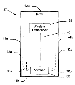
Referring initially to FIGS. I through 4, a mobile wireless communications
device,
such as a cellular telephone 20, is for a user 21. In some applications, the
user 21 may be
wearing an electronic hearing aid 22 in an ear 23 of the user. In particular,
the cellular
telephone 20 may advantageously provide desired hearing aid compatibility
(HAC) for
users with hearing aids in some implementations, as will be discussed further
below, but
need not be used with hearing aids in all embodiments.
The cellular telephone 20 illustratively includes a portable housing 24 and an
audio
output transducer 28 (e.g., a speaker) carried by the housing and accessible
to the
electronic hearing aid 22 of the user 21 adjacent the top of the housing as
shown. An audio
input transducer (e.g., microphone) is also carried by the housing 24 and
accessible to a
mouth 31 of the user 21 adjacent the bottom of the housing. Although described
herein
with reference to a cellular device, it should be noted that the present
disclosure may be
applicable to other wireless communications devices such as wireless LAN
devices, etc.
The cellular telephone 20 further illustratively includes a printed circuit
board
(PCB) 37 carried by the housing 24, and an antenna 35 and a wireless (e.g.,
cellular)
transceiver 38 carried on a front and/or back surface of the PCB. Of course,
these
components may be carried on the back surface or in positions other than those
shown in
other embodiments. The PCB 37 further illustratively includes an antenna feed
line 40
connecting the antenna 35 to the wireless transceiver 38. By way of example,
the antenna
35 may be formed by a plurality of conductive traces on the PCB 37 and may
take the
form of one or more single or multi-feed point antenna elements (monopole,
inverted F,
etc., for example, as will be appreciated by those skilled in the art. The
cellular telephone
20 may further include other components connected to the PCB 37 such as a
display,
battery 53 (FIG. 4), keypad, processing circuitry, etc., as will be discussed
further below.
In the present example, the antenna 35 is positioned adjacent a bottom 42b of
the
PCB 37 and therefore the bottom of the housing 24 (i.e., where the input
microphone is),
which advantageously helps reduce coupling to the electronic hearing aid 22 of
the user 21
with respect to traditional top-mounted, internal cellular phone antennas. The
PCB 37 also
has left and right sides 41a, 41b as well as a top 42a. This is because the
electronic hearing
aid 22 of the user 21 is advantageously further separated from the antenna 35
when the
cellular telephone 20 is held adjacent the user's ear 23 than would otherwise
be the case
with a typical top-mounted, internal cellular telephone antenna, for example.
Moreover,
CA 02633391 2008-06-20
this antenna placement also helps space the antenna 35 farther apart from the
user's brain,
which in turn helps to reduce the SAR of the cellular telephone 20 again with
a respect to
a traditional top-mounted, internal cellular phone antenna. However, it should
be noted
that a top-mounted or other antenna placement may be used in some embodiments.
Nonetheless, if the portable housing 24 has a relatively small form factor or
footprint for user convenience, this means that the antenna 35 may still be
positioned
relatively close to the user's ear 23, thus potentially elevating the SAR or
coupling to the
hearing aid 22 to unacceptable levels. As such, the cellular telephone 20 may
therefore
advantageously include first and second pairs of electrically floating,
electrically
conductive, antenna beam shaping elements 30a, 30b and 32a, 32b for helping to
direct the
beam pattern of the antenna 35 away from the user and the hearing aid 22, as
will be
appreciated by those skilled in the art. The first and second pairs of beam
shaping
elements 30a, 30b and 32a, 32b advantageously define a two-stage antenna
coupling
configuration. It should be noted that additional pairs of beams shaping
elements may also
be used in some embodiments.
Generally speaking, the first pair of antenna beam shaping elements 30a, 30b
are
positioned in an offset relationship relative to the second pair of antenna
beam shaping
elements 32a, 32b. In the present example, the two pairs are laterally offset
from one
another. That is, they are laterally offset or spaced apart from one another
from left to right
in the plane of the page. Moreover, the first and second pairs of antenna beam
shaping
elements 30a, 30b and 32a, 32b may be co-planar, e.g., on a same side of the
PCB 37
(which may or may not be the same side of the PCB that the antenna 35 is on),
on a same
surface of the portable housing 24, etc. In other embodiments, the first and
second pairs of
antenna beam shaping elements 30a, 30b and 32a, 32b may be on different sides
of the
PCB 37, or one may be positioned on the PCB and the other carried on a surface
of the
housing 24, for example. Other configurations are also possible, as will be
appreciated by
those skilled in the art, and as will be discussed further below.
By way of example, the first and second pairs of antenna beam shaping elements
30a, 30b and 32a, 32b may be symmetrically positioned with respect to the
antenna 35.
More particularly, the present example each of the first and second pairs of
antenna beam
shaping elements 30a, 30b and 32a, 32b are positioned substantially parallel
to a
longitudinal axis 36 of the portable housing, as shown in FIG. 3, although
other
6
CA 02633391 2008-06-20
placements may also be possible in different embodiments, as will be
appreciated by those
skilled in the art.
Each of the first pair of antenna beam shaping elements 30a, 30b may have a
first
length, and each of the second pair of antenna beam shaping elements 32a, 32b
may have
a second length. In the illustrated embodiment, the second length is greater
than the first
length, although it could be the opposite in other embodiments (or the first
and second
lengths could be the same). By way of example, each beam shaping element 30a,
30b, 32a,
32b may have a width in a range of about 2 to 15 mm, and a length in a range
of about 1 to
cm, although other sizes may also be used in some embodiments.
As will be appreciated by those skilled in the art, the size, number, and
placement
of the first and second pairs of antenna beam shaping elements 30a, 30b and
32a, 32b will
have an effect on the performance of the antenna 35. Thus, the particular
size/number/placement selection may vary depending upon the given
implementation and
the applicable antenna performance characteristics. It should also be noted
that the second
pair of beam shaping 32a, 32b need not be longer than the first pair in all
embodiments
(i.e., the pairs may be the same length or the second pair shorter than the
first).
As shown in FIG. 4, the cellular telephone 20 illustratively includes a
battery 53
carried within the portable housing 24 and removably connected to the PCB 37,
and a
removable access panel 50 provides access to the battery. A release button or
catch 51 (or
other suitable element) may be included for securing the panel 50 in place. In
the
illustrated embodiment, the first pair of antenna beam shaping elements 30a,
30b is
secured to the inner surface of the removable access panel 50, and the second
pair of beam
shaping elements 32a, 32b are carried on the inner surface of the back side of
the portable
housing directly adjacent the removable access panel. The use of such a two-
stage beam
shaping element configuration advantageously allows the configuration to be
adapted to
different form factors and housing shapes/sizes. That is, the first and second
pairs of beam
shaping elements 30a, 30b and 32a, 32b can advantageously be positioned to
accommodate different shapes and sizes of battery access panels 50 and form
factors, as
will be appreciated by those skilled in the art. In some embodiments, one or
both pairs of
the beam shaping elements may also be positioned on the sides of the housing
24.
In the exemplary embodiment, the beam shaping elements 30a, 30b and 32a, 32b
are generally rectangular metal layers that are secured to the inner surfaces
of the access
7
CA 02633391 2008-06-20
panel 50 and portable housing 24, respectively, with an adhesive layer.
However, the beam
shaping elements 30a, 30b and 32a, 32b may take different shapes in different
embodiments, and may be secured to the housing 24, access panel 50, PCB 37,
etc. by
suitable methods of attachment other than an adhesive. For example, the beam
shaping
elements 30a, 30b may be printed on the housing/access panel/PCB with
conductive ink,
similar to conductive circuit traces on a circuit board, as will be
appreciated by those
skilled in the art.
In some embodiments, it may be desirable to place a cover layer (not shown) on
or
more of the beam shaping elements 30a, 30b, 32a, 32b, and particularly if the
element(s) is
going to be placed on an outside surface of the portable housing 24. The cover
layer may
be a dielectric layer, such as a dielectric tape layer, for example. The cover
layer(s) may
advantageously help protect the beam shaping elements so that they are not
damaged or
altered such that SAR and/or HAC performance is potentially degraded.
Moreover, the
cover layer(s) may also advantageously conceal the beam shaping elements, for
example,
by making the cover layer the same color as a color of the portable housing 24
and/or the
access panel 50, as will be appreciated by those skilled in the art.
Referring now to FIG. 5, an alternative embodiment is shown in which the
second
pair of beam shaping elements 32a', 32b' are positioned between the first pair
of beam
shaping elements. As can be seen in the present embodiment and the embodiment
discussed above, the first pair of beam shaping elements 30a', 30b' have
respective ends
that extend beyond respective ends of the second pair of beam shaping elements
32a',
32b'. However, in some embodiments the ends may be co-terminus, or the ends
need not
extend all the way to one another.
Still another alternative embodiment is now described with reference to FIGS.
6
and 7. Here, the first pair of beam shaping elements 30a", 30b" are positioned
in a
vertically offset relationship relative to the second pair of beam shaping
elements 32a",
32b", as perhaps best seen in FIG. 7. Stated alternatively, the first pair of
beam shaping
elements 30a", 30b" are positioned vertically above the antenna 35", and the
second pair
of beam shaping elements 32a", 32b" are positioned vertically above the first
pair of
beam shaping elements.
In the illustrated example, this is accomplished by positioning the first pair
of
beam shaping elements 30a", 30b" on the inner surface of the front side of the
portable
8
CA 02633391 2008-06-20
housing 24", and the second pair of beam shaping elements 32a", 32b" is
positioned on
the outer surface of the front side of the portable housing, as shown.
However, in other
embodiments the first and/or second pairs of beam shaping elements 30a", 30b"
and
32a", 32b" could be positioned vertically beneath the antenna 35" (e.g., on
the back side
of the PCB 37" and/or inner/outer surfaces of the back side of the portable
housing 24").
In the present example, the first and second pairs of beam shaping elements
30a", 30b"
and 32a", 32b" also partially overlap, but as noted above an overlap is not
required in all
embodiments.
Other exemplary components of a hand-held mobile wireless communications
device 1000 are now described in the example below with reference to FIG. 8.
The device
1000 illustratively includes a housing 1200, a keypad 1400 and an output
device 1600.
The output device shown is a display 1600, which is preferably a full graphic
LCD. Other
types of output devices may alternatively be utilized. A processing device
1800 is
contained within the housing 1200 and is coupled between the keypad 1400 and
the
display 1600. The processing device 1800 controls the operation of the display
1600, as
well as the overall operation of the mobile device 1000, in response to
actuation of keys on
the keypad 1400 by the user.
The housing 1200 may be elongated vertically, or may take on other sizes and
shapes (including clamshell housing structures). The keypad may include a mode
selection
key, or other hardware or software for switching between text entry and
telephony entry.
In addition to the processing device 1800, other parts of the mobile device
1000 are
shown schematically in FIG. 8. These include a communications subsystem 1001;
a short-
range communications subsystem 1020; the keypad 1400 and the display 1600,
along with
other input/output devices 1060, 1080, 1100 and 1120; as well as memory
devices 1160,
1180 and various other device subsystems 1201. The mobile device 1000 is
preferably a
two-way RF communications device having voice and data communications
capabilities.
In addition, the mobile device 1000 preferably has the capability to
communicate with
other computer systems via the Internet.
Operating system software executed by the processing device 1800 is preferably
stored in a persistent store, such as the flash memory 1160, but may be stored
in other
types of memory devices, such as a read only memory (ROM) or similar storage
element.
In addition, system software, specific device applications, or parts thereof,
may be
9
CA 02633391 2008-06-20
temporarily loaded into a volatile store, such as the random access memory
(RAM) 1180.
Communications signals received by the mobile device may also be stored in the
RAM
1180.
The processing device 1800, in addition to its operating system functions,
enables
execution of software applications 1300A-1300N on the device 1000. A
predetermined set
of applications that control basic device operations, such as data and voice
communications 1300A and 1300B, may be installed on the device 1000 during
manufacture. In addition, a personal information manager (PIM) application may
be
installed during manufacture. The PIM is preferably capable of organizing and
managing
data items, such as e-mail, calendar events, voice mails, appointments, and
task items. The
PIM application is also preferably capable of sending and receiving data items
via a
wireless network 1401. Preferably, the PIM data items are seamlessly
integrated,
synchronized and updated via the wireless network 1401 with the device user's
corresponding data items stored or associated with a host computer system.
Communication functions, including data and voice communications, are
performed through the communications subsystem 1001, and possibly through the
short-
range communications subsystem. The communications subsystem 1001 includes a
receiver 1500, a transmitter 1520, and one or more antennas 1540 and 1560. In
addition,
the communications subsystem 1001 also includes a processing module, such as a
digital
signal processor (DSP) 1580, and local oscillators (LOs) 1601. The specific
design and
implementation of the communications subsystem 1001 is dependent upon the
communications network in which the mobile device 1000 is intended to operate.
For
example, a mobile device 1000 may include a communications subsystem 1001
designed
to operate with the MobitexTM, Data TACTM or General Packet Radio Service
(GPRS)
mobile data communications networks, and also designed to operate with any of
a variety
of voice communications networks, such as AMPS, TDMA, CDMA, WCDMA, PCS,
GSM, EDGE, etc. Other types of data and voice networks, both separate and
integrated,
may also be utilized with the mobile device 1000. The mobile device 1000 may
also be
compliant with other communications standards such as 3GSM, 3GPP, UMTS, etc.
Network access requirements vary depending upon the type of communication
system. For example, in the Mobitex and DataTAC networks, mobile devices are
registered on the network using a unique personal identification number or PIN
associated
CA 02633391 2008-06-20
with each device. In GPRS networks, however, network access is associated with
a
subscriber or user of a device. A GPRS device therefore requires a subscriber
identity
module, commonly referred to as a SIM card, in order to operate on a GPRS
network.
When required network registration or activation procedures have been
completed,
the mobile device 1000 may send and receive communications signals over the
communication network 1401. Signals received from the communications network
1401
by the antenna 1540 are routed to the receiver 1500, which provides for signal
amplification, frequency down conversion, filtering, channel selection, etc.,
and may also
provide analog to digital conversion. Analog-to-digital conversion of the
received signal
allows the DSP 1580 to perform more complex communications functions, such as
demodulation and decoding. In a similar manner, signals to be transmitted to
the network
1401 are processed (e.g. modulated and encoded) by the DSP 1580 and are then
provided
to the transmitter 1520 for digital to analog conversion, frequency up
conversion, filtering,
amplification and transmission to the communication network 1401 (or networks)
via the
antenna 1560.
In addition to processing communications signals, the DSP 1580 provides for
control of the receiver 1500 and the transmitter 1520. For example, gains
applied to
communications signals in the receiver 1500 and transmitter 1520 may be
adaptively
controlled through automatic gain control algorithms implemented in the DSP
1580.
In a data communications mode, a received signal, such as a text message or
web
page download, is processed by the communications subsystem 1001 and is input
to the
processing device 1800. The received signal is then further processed by the
processing
device 1800 for an output to the display 1600, or alternatively to some other
auxiliary UO
device 1060. A device user may also compose data items, such as e-mail
messages, using
the keypad 1400 and/or some other auxiliary I/O device 1060, such as a
touchpad, a rocker
switch, a thumb-wheel, or some other type of input device. The composed data
items may
then be transmitted over the communications network 1401 via the
communications
subsystem 1001.
In a voice communications mode, overall operation of the device is
substantially
similar to the data communications mode, except that received signals are
output to a
speaker 1100, and signals for transmission are generated by a microphone 1120.
Alternative voice or audio I/O subsystems, such as a voice message recording
subsystem,
11
CA 02633391 2008-06-20
may also be implemented on the device 1000. In addition, the display 1600 may
also be
utilized in voice communications mode, for example to display the identity of
a calling
party, the duration of a voice call, or other voice call related information.
The short-range communications subsystem enables communication between the
mobile device 1000 and other proximate systems or devices, which need not
necessarily
be similar devices. For example, the short-range communications subsystem may
include
an infrared device and associated circuits and components, or a BluetoothTM
communications module to provide for communication with similarly-enabled
systems
and devices.
Many modifications and other embodiments will come to the mind of one skilled
in the art having the benefit of the teachings presented in the foregoing
descriptions and
the associated drawings. Therefore, it is understood that various
modifications and
embodiments are intended to be included within the scope of the appended
claims.
12