Note: Descriptions are shown in the official language in which they were submitted.
CA 02633461 2008-06-17
WO 2007/071064 PCT/CA2006/002117
-1-
SOLAR CELL WITH PHYSICALLY SEPARATED DISTRIBUTED
ELECTRICAL CONTACTS
BACKGROUND OF THE INVENTION
1. Field of Invention
This invention relates to solar cells and more particularly to semiconductor
photovoltaic cells and a process for forming electrical contacts in a solar
cell
structure.
2. Description of Related Art
It is well-known that under light illumination, photovoltaic (PV) solar cells
comprising semiconductor wafers generate electric current. This electric
current may be collected from the cell by means of front and back side
metallization on the wafer which acts as electrical contacts on front and back
sides of the solar cell. A partially electrically conductive paste, which
typically
contains silver and/or aluminum, is screen printed onto front and back
surfaces of the cell through a mask. For the front (active) side of the solar
cell
structure, the mask typically has openings through which the paste contacts
the surface to be metallized. The configuration of the openings determines the
shape of a pattern that the paste will form on the surface of the cell and the
ultimate shape of the electrical contacts. The front side mask is typically
configured to produce a plurality of thin parallel line contacts and two or
more
thicker lines that are connected to and extend generally perpendicular to the
parallel line contacts.
After spreading paste on the mask, the mask is removed and the wafer
bearing the partially conductive paste is initially heated such that the paste
dries. Later, the wafer is "fired" in an oven and the paste enters a metallic
phase and at least part of it diffuses through the front side surface of the
solar
cell and into the cell structure while a portion is left solidified on the
front side
surface. The multiple thin parallel lines thus form thin parallel linear
electrical
contacts referred to as "fingers", intersected by thicker perpendicular lines
CA 02633461 2008-06-17
WO 2007/071064 PCT/CA2006/002117
-2-
referred to as "bus bars". The purpose of the fingers is to collect the
electrical
current from the front side of the PV cell. The purpose of the bus-bars is to
receive the current from the fingers and transfer it away from the cell.
Typically, the width and the height of each finger is approximately 120
microns and 10 micron respectively. Inherent technical limitations of screen
printing technology further introduce 1-10 micron fluctuations in finger
height
and 10-30 micron or greater fluctuations in width. While the fingers are
sufficient to harvest small electric currents, the bus-bars are required to
collect
a much greater current from the plurality of fingers and therefore have a
substantially larger cross section and width.
Back side metallization involves a layer of partially conductive paste
containing aluminum over the entire back surface of the cell except for a few
small areas. During the initial heating, the paste dries. Then silver/aluminum
paste is screen printed in certain areas that have not been printed with
aluminum paste and is further dried. Then, when the wafer is subjected to
"firing", wherein the aluminum paste forms a passivation layer called a Back
Surface Field (BSF) and aluminum contacting layer and the silver/aluminum
paste forms silver/aluminum pads. The aluminum contacting layer collects the
electrical current from the PV cell itself and passes it to the silver pads.
The
silver/aluminum pads are used to take the electric current away from the PV
cell.
The area that is occupied by the fingers and bus bars on the front side of the
solar cell is known as the shading area and prevents solar radiation from
reaching the solar cell surface. This shading area decreases solar cell
conversion efficiency. Modern solar cell shading occupies 6-10% of the
available solar cell surface area.
In addition, the presence of metallization on the front side and the
silver/aluminum pads on the back side results in a decrease of voltage
CA 02633461 2008-06-17
WO 2007/071064 PCT/CA2006/002117
-3-
generated by the PV cell proportionate to the metallization area. Therefore,
in
order to achieve maximum conversion efficiency of the PV cell, it is desirable
to minimize the area occupied by front side metallization. In addition, it is
also
desirable to minimize the area of silver metallization on the back side, in
particular, to reduce the amount of silver/aluminum paste required. This will
increase cell efficiency and will substantially decrease the cost of solar
cell
fabrication because silver/aluminum paste can be expensive.
The use of modern screen printing technology for front side metallization
achieves a certain minimal level of metallization by optimizing widths and
thicknesses of fingers and bus-bars for the solar cell being produced.
However, there are principle limitations that prevent further decreases of the
metallization area. Firstly, the cross sectional dimensions of the fingers
cannot be less than certain dimensions in order to avoid excessive resistive
losses due to electric current flow through the fingers during solar cell
operation. In addition, bus bars are required to have minimum cross-sectional
dimensions also to avoid resistive losses during operation. In addition,
conventional technology does not allow eliminating the silver/aluminum pads
on the rear side of the solar cell because PV module production requires the
solar cells to be interconnected in-series via tinned copper tabs soldered to
the silver/aluminum pads.
Several papers describe methods for printing very narrow fingers of :570
micron width (B. Raabe, F. Huster, M. McCann, P. Fath, HIGH ASPECT
RATIO SCREEN PRINTED FINGERS, Proc. of the 20th European
Photovoltaic Solar Energy Conference, 6-10 June 2005, Barcelona, Spain;
Jaap Hoornstra, Arthur W. Weeber, Hugo H.C. de Moor, Wim C. Sinke, THE
IMPORTANCE OF PASTE RHEOLOGY IN IMPROVING FINE LINE, THICK
FILM SCREEN PRINTING OF FRONT SIDE METALLIZATION, Proc. of the
14th European Photovoltaic Solar Energy Conference, 30.06-04.07 1997,
Barcelona, Spain; and A.R. Burgers, H.H.C. de Moor, W.C. Sinke, P.P.
Michiels, INTERRUPTION TOLERANCE OF METALLIZATION PATTERNS,
CA 02633461 2008-06-17
WO 2007/071064 PCT/CA2006/002117
-4-
Proc. of the 12 th European Photovoltaic Solar Energy Conference, 11-15 April
1994, Amsterdam, The Netherlands). Unfortunately, conventional fingers of
<_70 microns have narrow cross sections that are too small to handle the
necessary level of electric current capable of being produced by the solar
cell
without excessive resistive losses. In order to achieve adequate finger
conductivity it may be necessary to either apply a second layer of screen
printed paste on top of the first one or to apply a layer of metal on top of
an
initial screen printed metallization, using galvanic technology. The resulting
cost and complexity of these methods add a prohibitively high expense to the
production of photocells.
Heretofore, there appears to be no simple way to produce a photovoltaic solar
cell having reduced front side shading and no conventional screen printed
silver/aluminum pads on the back side.
SUMMARY OF THE INVENTION
In accordance with one aspect of the invention, there is provided a
photovoltaic apparatus. The apparatus includes a semiconductor photovoltaic
cell structure having a front side surface and a back side surface provided by
respectively doped portions of semiconductor material forming a photovoitaic
junction. The apparatus further includes a plurality of electrical contacts
embedded in the front surface of a respective one of the portions of
semiconductor material, the electrical contacts being distributed in two
dimensions across the surface and separated from each other and in
electrical contact with the respective one of the portions of semiconductor
material. The apparatus further includes a back side electrical contact on the
back surface of the other of the respective portions of semiconductor material
and in electrical contact therewith.
The electrical contacts may be distributed in two orthogonal directions across
the surface.
CA 02633461 2008-06-17
WO 2007/071064 PCT/CA2006/002117
-5-
The electrical contacts may be distributed evenly in the two orthogonal
directions.
The electrical contacts may be arranged in an array.
The electrical contacts may be arranged in rows and columns.
Contacts of alternate rows may be arranged to lie in positions adjacent
spaces between contacts in adjacent rows.
Generally each of the electrical contacts may have a contact surface facing
generally normal to the front side surface and operable to be connected to a
conductor.
The contact surface may have a generally rectangular shape.
The contact surface may have a generally circular shape.
The contact surface may have a star shape.
A solar cell apparatus may be made from the photovoltaic apparatus and may
further include a first electrode for contacting the electrical contacts. The
first
electrode may include an electrically insulating optically transparent film
having a surface, an adhesive layer on the surface of the film, at least one
electrical conductor embedded into the adhesive layer, a conductor surface of
the electrical conductor protruding from the adhesive layer, and an alloy
bonding the electrical conductor to at least some of the electrical contacts
such that current collected from the solar cell by the electrical contacts is
gathered by the electrical conductor.
The electrical conductor may be connected to a common bus.
CA 02633461 2008-06-17
WO 2007/071064 PCT/CA2006/002117
-6-
The electrical contacts may be arranged in rows and columns. The electrode
may include a plurality of electrical conductors arranged in parallel spaced
apart relation and the electrical conductors may be in contact with a
plurality
of the electrical contacts in a respective row or column.
Each of the electrical conductors may be connected to a bus.
The solar cell apparatus may further include a second electrode for contacting
the back side electrical contact. The second electrode may include a second
electrically insulating film having a second surface, a second adhesive layer
on the second surface of the second film, at least one second electrical
conductor embedded into the second adhesive layer, a second conductor
surface of the second electrical conductor protruding from the second
adhesive layer, and a second alloy bonding the second electrical conductor to
the back side electrical contact such that current received at the solar cell
from the back side electrical contact is provided by the electrical conductor.
In accordance with another aspect of the invention, there is provided a
process for forming contacts in a semiconductor photovoltaic cell structure.
The process includes distributing a plurality of individual portions of
electrical
contact paste in two dimensions across a front side surface of a
semiconductor photovoltaic cell structure comprising respective doped
portions of semiconductor material forming a photovoltaic junction; causing
the individual portions of electrical contact paste to become embedded in the
front side surface such that the individual portions of electrical contact
paste
form respective separate electrical contacts in the front side surface, the
separate electrical contacts being in electrical contact with a corresponding
doped portion of semiconductor material; and forming a back side electrical
contact on a back side surface provided by the other of the respective
portions of semiconductor material and in electrical contact therewith.
CA 02633461 2008-06-17
WO 2007/071064 PCT/CA2006/002117
-7-
Distributing may include printing the individual portions of electrical
contact
paste on the front side surface.
Printing may include screen printing.
Distributing may include distributing the individual portions of electrical
contact
paste in two orthogonal directions across the surface.
Distributing may include distributing the individual portions of electrical
contact
paste evenly in the two orthogonal directions.
Distributing may include distributing the individual portions of electrical
contact
paste in an array.
Distributing may include distributing the individual portions of electrical
contact
paste in rows and columns.
Distributing may include causing the individual portions of electrical contact
paste in alternate rows to lie in positions adjacent spaces between contacts
in
adjacent rows.
Causing the individual portions of electrical contact paste to become
embedded in the front side surface may inciude heating the semiconductor
photovoltaic cell structure with the portions of electrical contact paste
thereon
for a sufficient time and at a sufficient temperature to permit at least some
of
the electrical contact paste of each individual portion of electrical contact
paste to enter a metallic phase and diffuse through the front side surface and
into the portion of semiconductor material below the front side surface while
leaving a sufficient portion of electrical contact paste in the metallic phase
at
the front side surface to act as an electrical contact surface of the separate
electrical contact so formed.
CA 02633461 2008-06-17
WO 2007/071064 PCT/CA2006/002117
-8-
The process may further include laying on the front side surface an electrode
comprising an electrically insulating optically transparent film having an
adhesive layer in which at least one electrical conductor is embedded such
that a conducting surface thereof bearing a coating comprising a low melting
point alloy protrudes from the adhesive layer, such that the conducting
surface contacts a plurality of the electrical contacts formed in the
semiconductor photovoltaic cell structure front side surface, and causing the
low melting point alloy to melt to bond the conducting surface to the
plurality
of electrical contacts to electrically connect the electrical contacts to the
electrical conductor to permit the electrical conductor to draw current from
the
solar cell through the electrical contacts.
The process may further include connecting the at least one electrical
conductor to a bus.
The electrical contacts may be arranged in rows and columns and the
electrode may include a plurality of electrical conductors arranged in
parallel
spaced apart relation. The electrode may be laid on the front side surface
such that each electrical conductor is in contact with a plurality of the
electrical
contacts in a respective row or column.
The process may further involve connecting each of the electrical conductors
to a common bus.
The process may further involve laying on the back side surface an electrode
made of a second electrically insulating film having a second adhesive layer
in
which at least one second electrical conductor is embedded such that a
second conducting surface thereof, bearing a second coating comprising a
second low melting point alloy protrudes from the second adhesive layer,
such that the second conducting surface contacts the back side electrical
contact formed on the semiconductor photovoltaic cell structure back side
surface and causing the second low melting point alloy to melt to bond the
CA 02633461 2008-06-17
WO 2007/071064 PCT/CA2006/002117
-9-
second conducting surface to the back side electrical contact to electrically
connect the back side electrical contact to the second electrical conductor to
permit the electrical conductor to supply current to the solar cell through
the
back side electrical contact.
Other aspects and features of the present invention will become apparent to
those ordinarily skilled in the art upon review of the following description
of
specific embodiments of the invention in conjunction with the accompanying
figures.
BRIEF DESCRIPTION OF THE DRAWINGS
In drawings which illustrate embodiments of the invention,
Figure 1 is a process diagram showing successive stages of a method for
forming contacts on a semiconductor wafer, according to a first
embodiment of the invention;
Figure 2 is a cross sectional view of a semiconductor photovoltaic cell
structure on which electrical contacts are to be formed by the
method of Figure 1;
Figure 3 is a cross-sectional/perspective view of an apparatus according to
an embodiment of another aspect of the invention, on which
electrical contacts have been formed by the process of Figure 1;
Figure 4 is a top view of the apparatus shown in Figure 3, showing
electrical contacts having a rectangular shape;
Figure 5 is a top view of an apparatus according to an alternate
embodiment of the invention in which electrical contacts are
circularly shaped;
CA 02633461 2008-06-17
WO 2007/071064 PCT/CA2006/002117
-10-
Figure 6 is a top view of an apparatus according to a third embodiment of
the invention in which electrical contacts are rectangular and
arranged in staggered rows;
Figure 7 is a top view of an apparatus according to a fourth embodiment of
the invention in which electrical contacts are circular and arranged
in staggered rows;
Figure 8 is a top view of an electrical contact having a star shape, in
accordance with another embodiment of the invention;
Figure 9 is a top view of an electrical contact having a cross shape in
accordance with another embodiment of the invention;
Figure 10 is a perspective view of an apparatus of the type shown in Figures
3, 4, 5, 6 or 7 showing electrodes being connected to front side
electrical contacts and a back side aluminum contact layer; and
Figure 11 is a side view of the apparatus shown in Figure 10 after first and
second electrodes have been affixed to said front side electrical
contacts and back side aluminum contact layer, respectively.
DETAILED DESCRIPTION
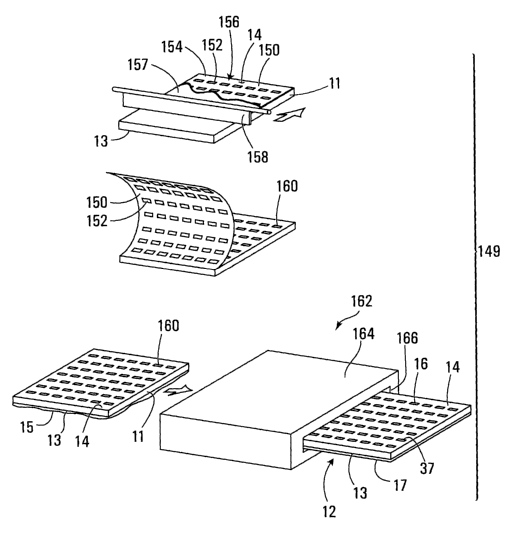
Referring to Figure 1, a method according to a first embodiment of a first
aspect of the invention, for forming electrical contacts in a semiconductor
photovoltaic cell structure 11 is shown generally at 149.
Semiconductor Photovoltaic Cell Structure
Referring to Figure 2, in this embodiment the semiconductor photovoltaic cell
structure 11 includes a silicon wafer into which has been diffused an n-type
region 20 and a p-type region 22 which form a p-n junction 23. Alternatively,
the n-type region 20 and the p-type region 22 may be reversed. In the
CA 02633461 2008-06-17
WO 2007/071064 PCT/CA2006/002117
-11-
embodiment shown, a front side surface 14 is provided by a surface of the n-
type region 20 and the p-type region 22 is immediately adjacent the n-type
region and defines a back side surface 13. In the embodiment shown, the n-
type region has a thickness of approximately 0.6 micrometers and the p-type
region has a thickness of approximately 200-600 micrometers.
Process for Forming Electrical Contacts
Referring back to Figure 1, the process for forming electrical contacts
involves
distributing a plurality of individual portions of electrical contact paste in
two
dimensions across a front side surface of the semiconductor photovoltaic cell
structure comprising respective doped portions of semiconductor material
forming a photovoltaic junction, and causing the individuai portions of
electrical contact paste to become embedded in the front side surface such
that the individual portions of electrical contact paste form respective
separate
electrical contacts in the front side surface. The separate electrical
contacts
are in electrical contact with a corresponding doped portion of semiconductor
material forming the photovoltaic junction. The process further involves
forming a back side electrical contact on the back side surface of the other
of
the respective portions of semiconductor material and in electrical contact
therewith.
The process may begin by printing the individual portions of electrical
contact
paste 157 on the front side surface 14 such as by screen printing. Printing
may involve screen printing wherein a mask 150 having a plurality of openings
152 arranged in a desired distribution, such as in an array of rows and
columns 154 and 156, for example, is made to receive an amount of electrical
contact paste 157 containing aluminum, silver, adhesive and silicon, in a
solvent. A spreader 158 is then drawn across the mask 150 such that the
paste 157 is distributed in two dimensions across the front side surface 14
through the openings 152 in the mask 150.
CA 02633461 2008-06-17
WO 2007/071064 PCT/CA2006/002117
-12-
The spreader 158 may be moved in two orthogonal directions at successive
points in time, for example, to distribute the electrical contact paste 157 in
the
two orthogonal directions across the front side surface 14. Automated
machinery may be used to cause the electrical contact paste 157 to be
distributed across the front side surface 14, through the openings 152 in the
mask 150.
Various opening shapes and arrangements may be employed in the mask
150 to distribute the electrical contact paste in any desired distribution
such as
evenly in the two orthogonal directions, unevenly in the two orthogonal
directions, in an array, in rows and columns, in staggered rows in which
alternate rows lie in positions adjacent spaces between openings in adjacent
rows, in gaussian distributions in one/or two directions, in distributions
providing an increasing density of openings toward one side and/or end of the
mask or any other distribution.
After the electrical contact paste has been distributed, the mask 150 may be
separated from the surface, leaving the distributed electrical contact paste
in
separate isolated islands as shown at 160, for example, in the desired pattern
of distribution, i.e., rows and columns, even rows and columns, uneven rows
and columns, staggered rows and columns, etc.
Then, the electrical contact paste 160 is heated until dry. When the paste 160
is dry, back side metallization paste 15 is applied to an entire back side
surface 13 of the structure 11 and is heated until dry. When both the
electrical
contact paste 160 and the back side metallization paste 15 have dried, the
individual portions of electrical contact paste 160 are caused to become
embedded in the front side surface 14 such that the individual portions of
electrical contact paste form respective separate electrical contacts in the
front side surface 14 and the back side metallization paste 15 is fused into
the
back side surface 13. In the embodiment shown, this action is shown
generally at 162 in which the semiconductor cell structure 11 with the
CA 02633461 2008-06-17
WO 2007/071064 PCT/CA2006/002117
-13-
distributed electrical contact paste 160 and back side metallization paste 15
thereon is passed through an oven 164 where it is heated for a sufficient time
and at a sufficient temperature to permit a small portion of the electrical
contact paste of each individual portion of electrical contact paste to enter
a
metallic phase and diffuse through the front side surface 14 and into the
semiconductor photovoltaic cell structure below, while leaving a sufficient
portion (nearly all) of electrical contact paste 160 in the metallic phase
exposed at the front side surface 14.
The electrical contact paste 160 forms electrical contacts 16 in the front
side
surface 14, the electrical contacts being in electrical contact with the n-
type
semiconductor material beneath the active side surface, but separate from
other contacts. Each electrical contact 16 has an electrical contact surface
37
formed by the portion of electrical contact paste 160 in the metallic phase
left
on the front side surface 14. The electrical contacts 16 are thus
intermittently
positioned across the front side surface 14.
Similarly, the back side metallization paste 15 is fused to a back side
surface
13 of the semiconductor photovoltaic cell structure 11 thereby creating a back
surface field and provides a back side electrical contact 17.
In the embodiment shown, the oven 164 has an outlet 166 through which a
compieted semiconductor photovoltaic cell apparatus 12, having a front side
surface 14 with a plurality of separate electrical contacts 16 embedded
therein
and a back side electrical contact 17 comprising a single large contact fused
therein is provided.
Semiconductor Photovoltaic Cell Apparatus
As a result of the process shown in Figure 1, a completed semiconductor
photovoltaic cell apparatus according to a first embodiment of the invention
is
produced, as shown generally at 12 in Figure 3. The apparatus 12 comprises
a semiconductor photovoltaic cell structure having a front side surface and a
CA 02633461 2008-06-17
WO 2007/071064 PCT/CA2006/002117
-14-
back side surface 13 provided by respective doped portions 20 and 22 of
semiconductor material forming a photovoltaic junction 23, a piurality of
electrical contacts 16 embedded in the front side surface 14 of the respective
one of the portions of semiconductor material. The electrical contacts 16 are
distributed in two dimensions across the surface 14, separated from each
other, and in electrical contact with the respective one of the portions of
semiconductor material. The apparatus further comprises a back side
electrical contact 17 on the back side surface of the other of the respective
portions of semiconductor material and in electrical contact therewith.
Referring to Figure 4, in the embodiment shown, the electrical contacts 16 of
the compieted semiconductor cell apparatus 12 are distributed in two
dimensions across the front side surface 14, the distribution being
established
by the mask 150 shown in Figure 1. The electrical contacts 16 are separate
from each other, aithough they are electrically connected to the
semiconductor photovoltaic structure under the front side surface 14.
In the embodiment shown the electrical contacts 16 are distributed in two
orthogonal directions, shown generally at 30 and 32 and, in this embodiment,
they are distributed evenly in these two directions. In other words, the
spacing
between the contacts in the first direction 30 is uniform and the spacing
between the contacts in the second direction 32 is also uniform. In the
embodiment shown, the contacts are arranged in rows and columns, a first
row being shown generally at 34 and a first column being shown generally at
36. The contacts are thus arranged in an array in this embodiment.
Alternatively, other distributions of contacts may have been laid by the mask
150 shown in Figure 1. For example, the density of contacts on the front side
surface 14 may increase in the first direction 30, in the second direction 32
or
in both directions. Or a gaussian or any other distribution in the first
and/or
second directions may be used.
CA 02633461 2008-06-17
WO 2007/071064 PCT/CA2006/002117
-15-
In the embodiment shown, the electrical contacts 16 have an electrical contact
surface 37 having an eiongated rectangular shape, having a length 38 of
between approximately 0.5 mm to approximately 2 mm and a width 40 of
between approximately 0.1 mm to 1 mm. In the embodiment shown, each
contact surface 37 has generally the same length and width dimensions and
is oriented in generally the same direction, i.e., aligned in the first
orthogonal
direction 30. It will be appreciated that each contact 16 is physically
isolated in
that it is set apart from each other electrical contact. However, each contact
16 is also in electrical contact with the n-type material under the front side
surface 14 to make electrical connection with the semiconductor photovoltaic
cell structure 11. Therefore, while the electrical contacts 16 appear
physically
separate when viewed from the front side surface 14 of the solar cell
structure, they are in fact electrically connected to the semiconductor
photovoltaic cell structure beneath the front side surface 14. In one sense,
the
contacts 16 appear to be intermittent "fingers" across the front side surface
14
rather than continuous linear fingers as in the prior art.
Referring to Figure 5, a semiconductor photovoltaic cell apparatus according
to a second embodiment of the invention is shown generally at 50. In this
embodiment, the semiconductor photovoltaic cell apparatus is identical to that
shown at 12 in Figure 3, with the exception that it has electrical contacts 52
with circularly shaped contact surfaces 53 instead of rectangular contacts as
shown in Figure 4.
Referring back to Figure 5, in this embodiment, each electrical contact 52 is
distributed in the same two orthogonal directions 30 and 32 across the
surface of the semiconductor photovoltaic structure and is distributed evenly
in these two orthogonal directions. Again, the electrical contacts 52 are
arranged in rows and columns, a first row being shown generally at 54 and a
first column being shown generally at 56. Also, in this embodiment, the
electrical contacts 52 are spaced apart by a distance 58 in the first
orthogonal
direction and a second distance 60 in the second orthogonal direction 32.
CA 02633461 2008-06-17
WO 2007/071064 PCT/CA2006/002117
-16-
These distances may be equal or different. Again, aiternatively, the contacts
52 may be distributed across the front side surface 14 with increasing density
in the first and/or second directions 30 and 32 or more generally with
constant
or changing density in these two directions.
As stated, each electrical contact 52 has a circular contact surface 53,
having
a diameter 62 of approximately 1 millimetre. Again, each electrical contact 52
is embedded in the front side surface 14 and into the n-type layer 20 of the
semiconductor photovoltaic cell structure 11. Circular openings in the mask
150 described in Figure 1, may be used to make electrical contacts having
circular contact surfaces 53 as shown.
Referring to Figure 6, a semiconductor photovoltaic cell apparatus according
to a third embodiment of the invention is shown generally at 70. This
apparatus 70 includes the same semiconductor photovoltaic cell structure 11
as shown in Figure 2 and includes a plurality of rectangular contacts, one of
which is shown at 72, distributed in the same two orthogonal directions 30 and
32 across the front side surface 14 of the semiconductor photovoltaic cell
structure. In this embodiment, the contacts 72 are arranged in a plurality of
staggered rows, one of which is shown generally at 74 and a second of which
is shown at 76. In this embodiment, there are spaces 78 between the contacts
72 of a given row, such as row 74, and the contacts of each row have the
same spacing 78. However, the contacts 72 of the second row 76 are
arranged to align approximately centrally between contacts in the adjacent
row, i.e., the first row 74. This is repeated throughout all rows of contacts
such
that the contacts of alternate rows are arranged to lie in positions adjacent
spaces between contacts in adjacent rows. In other words, adjacent rows are
staggered by a distance 79. The dimensions and spacing of the individual
rectangular contacts 72 have the same shape, dimensions and spacing as the
contacts 16 in Figure 4.
CA 02633461 2008-06-17
WO 2007/071064 PCT/CA2006/002117
-17-
Referring to Figure 7, a semiconductor photovoltaic cell structure apparatus
according to a fourth embodiment of the invention is shown generally at 80.
The apparatus 80 of this embodiment is similar to that of the embodiment
described above (in Figure 6) in that it includes contacts 82 that are
arranged
in staggered rows, one of which is shown at 84 and a second of which is
shown at 86, such that the contacts of alternate rows are arranged to lie in
positions adjacent spaces between contacts in adjacent rows. Otherwise, the
contacts 82 in any given row shown in Figure 7 have the same shape,
dimensions and spacing as the contacts 52 shown in Figure 5.
Referring to Figures 8 and 9, the contact surfaces of the electrical contacts
may have a star shape such as shown at 81 in Figure 8, an x shape as shown
at 83 in Figure 9, or any other desired shape that is surrounded on all sides
by
a void, space, insulator or semiconductor between it and the next nearest
contact.
Solar Cell Unit
Referring to Figure 10, a semiconductor photovoltaic cell apparatus according
to any of the apparatuses described in Figures 3 through 7 may be made into
a "solar cell unit" and connectable to an electrical circuit by securing a
first
electrode such as shown at 92 to the front side surface 14 to contact the
electrical contacts 72 and by securing a second electrode 93 to the back side
electrical contact 17.
In the embodiment shown in Figure 10, the first electrode 92 comprises an
electrically insulating optically transparent film 94 having a surface 96 and
an
adhesive layer 98 on the surface. The electrode 92 further includes at least
one electrical conductor 100 embedded into the adhesive layer 98 and having
a conductor surface 102 protruding from the adhesive layer. An alloy 104 is
used to bond the electrical conductor 100 to at least some of the electrical
contacts 72 such that current collected from the semiconductor photovoltaic
CA 02633461 2008-06-17
WO 2007/071064 PCT/CA2006/002117
-18-
cell apparatus by the electrical contacts is gathered by the electrical
conductor.
In the embodiment shown, the alloy bonding the electrical conductor 100 to at
least some of the electrical contacts may include a material that may be
heated to solidify and electrically bond and connect the electrical conductor
100 to a plurality of electrical contacts 72 in a row. The alloy may be a
coating
on the conductor surface 102, for example.
As shown in Figure 10, the electrode 92 includes a plurality of conductors
including conductor 100 and conductors 112, 114 and 116. The conductors
100, 112, 114 and 116 are, in this embodiment, laid out in parallel spaced
apart relation on the adhesive layer of the electrode with the spacing
corresponding to the spacing 78, for example, between adjacent columns 36,
118, 120 and 122 of contacts on the front side surface 14 of the
semiconductor cell apparatus 12. In effect therefore, in this embodiment the
electrical contacts 72 are arranged in rows and columns and the electrode 92
comprises a plurality of electrical conductors 100, 112, 114 and 116 arranged
in parallel spaced apart relation such that when the electrode is applied to
the
front side surface 14 of the semiconductor cell apparatus 12, the electrical
conductors are in contact with a plurality of electrical contacts 72 in a
respective column 36, 118, 120 and 122.
Initially, the first electrode 92 may be curled as shown in Figure 10 to align
a
rear edge 106 of the electrode with a rear edge 108 of the semiconductor cell
apparatus 12 and then the film 94, with its adhesive layer 98 with the
conductors 100, 112, 114 and 116 embedded therein, may be pressed
downwardly onto the front side surface 14 of the semiconductor cell apparatus
12 to roll out the electrode 92 and secure the adhesive layer to the front
side
surface 14, such that the electrical conductors 100, 112, 114 and 116 come
into contact with successive electrical contacts 72 of respective columns of
CA 02633461 2008-06-17
WO 2007/071064 PCT/CA2006/002117
-19-
contacts between the rear edge 108 of the semiconductor cell structure and a
front edge 111 of the semiconductor photovoltaic apparatus.
Alternatively, the rear edge 106 of the first electrode 92 may be aligned with
a
right hand side edge 124 of the semiconductor cell apparatus 12 and rolled
out across the front side surface 14 of the semiconductor cell apparatus in a
manner such that the conductors 100, 112, 114 and 116 contact a plurality of
electrical contacts 72 in a respective row of electrical contacts 72 on the
front
side surface 14 of the semiconductor cell apparatus 12.
In the embodiment shown, the electrical conductors 100, 112, 114 and 116
extend beyond the optically transparent film 94 and are terminated in contact
with a common bus 107, which may be formed of metallic foil, such as copper,
for example.
Further details of general and alternate constructions of the first electrode
92
may be obtained from applicant's International Patent Application published
under International Publication Number WO 2004/021455A1, which is
incorporated herein by reference.
The second electrode 93 is similar to the first electrode 92 in all respects
and
in fact a plurality of the above described first electrodes may be pre-
manufactured and individual ones applied to the front side surface 14 or back
side electrical contact 17 as desired. It should be noted however that the
second electrode 93 need not be optically transparent like the first electrode
since the back side is not intended to receive light.
The back side electrical contact 17 has no rows of contacts, but rather is a
single flat planar contact extending across the entire back side surface 13 of
the semiconductor cell structure. The conductors 100, 112, 114 and 116 of
the second electrode 93 are prepared with the low melting point alloy paste
and the electrode 93 is adhesively secured to the back side electrical contact
CA 02633461 2008-06-17
WO 2007/071064 PCT/CA2006/002117
-20-
17 such that the low melting point alloy is operable to bond the conductors to
the back side electrical contact 17 when sufficiently heated.
As shown in Figure 11, the second electrode 93 may be applied to the back
side electrical contact 17 such that a bus 95 thereof will lie adjacent the
rear
edge 108 of the semiconductor cell apparatus 12 while the bus 107 of the first
electrode 92 is located adjacent the front edge 110 of the semiconductor cell
apparatus 12. This permits adjacent solar cell structures to be connected in
series, for example, simply by placing them adjacent to each other and
allowing the bus bars 95 and 107 of adjacent semiconductor cell structures to
overlap each other, in contact with each other.
After the first electrode 92 is laid on top of the front side surface 14 such
that
the conductors 100, 112, 114 and 116 contact respective columns 36, 118,
120 and 122 of contacts 72, for example, and the second electrode 93 is laid
on the back side electrical contact 17, the resulting apparatus may be
regarded as an assembly. The assembly is then heated such that the low
melting point alloy associated with the first electrode 92 is caused to melt
to
bond the conducting surfaces of respective conductors 100, 112, 114 and 116
of the first electrode 92 to contact surfaces of respective rows of electrical
contacts 72 to electrically connect the electrical contacts to the electrical
conductors and to cause the low melting point alloy associated with the
second electrode 93 to bond the conducting surfaces of respective conductors
to the back side electrical contact 17, to permit the electrical conductors to
pass current through the solar cell through the electrical contacts. Once the
low melting point alloy has completed this bonding, a completed solar cell as
shown at 10 in Figure 11 ready to be used in an electrical circuit and has
thus
been produced.
A solar cell produced as described above may provide several advantages.
Due to the reduced area occupied by the electrical contacts in the front side
surface, there is less shading of the p-n junction which can cause as much as
CA 02633461 2008-06-17
WO 2007/071064 PCT/CA2006/002117
-21-
5-10 % more electric current to pass through the solar cell. In addition, as
there is less area occupied by metallization and the back surface field area
is
not interrupted by silver/aluminum fingers, the cell can generate a voltage of
up to 3 % more than conventional cells. Overall these two effects may
increase the efficiency of the solar cell by up to 10-15%. Furthermore, the
production costs of solar cells of the type described are lower than with
conventional solar cells because a substantially less amount of silver is used
in forming contacts.
While specific embodiments of the invention have been described and
illustrated, such embodiments should be considered illustrative of the
invention only and not as limiting the invention as construed in accordance
with the accompanying claims.