Note: Descriptions are shown in the official language in which they were submitted.
CA 02633889 2008-06-10
WO 2007/111709 PCT/US2006/061044
050168
1
PSEUDO-DUAL PORT MEMORY
HAVING A CLOCK FOR EACH PORT
BACKGROUND
Field
[0001] The disclosed embodiments relate generally to pseudo-dual port
memories.
Background
[0002] Dual port memories typically have two ports and an array of memory
cells. The
memory array can be simultaneously accessed from both of the ports provided
that the
memory cells being accessed from one port are not the same memory cells that
are
being accessed from the other port. A common type of memory cell used in such
dual
port memories involves eight field effect transistors (FETs). Four of the
transistors are
interconnected to form two cross-coupled inverters. A first data node D of the
memory
cell is the node at the output lead of a first of the inverters and the input
lead of the
second of the inverters. A second data node DN of the memory cell is the node
at the
output lead of the second of the inverters and the input lead of the first of
the inverters.
There are two access transistors coupled to the first data node D. The first
access
transistor is provided so that a first bit line B1 can selectively be coupled
to the first data
node D. The second access transistor is provided so that a second bit line B2
can
selectively be coupled to the first data node D. Similarly, there are two
access
transistors coupled to the second data node DN. The first access transistor is
provided
so that a first bit line bar BIN can be coupled to the second node DN. The
second
access transistor is provided so that a second bit line bar B2N can be coupled
to the
second node DN. The first bit line Bl and first bit line bar BIN constitute a
bit line pair
and a for coupling an addressed memory cell to a first of the two ports of the
dual port
memory. The second bit line B2 and second bit line bar B2N constitute a bit
line pair
and are for coupling an addressed memory cell to a second of the two ports of
the dual
port memory.
[0003] The memory cells in a single port memory typically only include six
transistors.
As in the case of the eight-transistor cell, four of the transistors form a
cross-coupled
inverter structure. Rather than there being two pairs of access transistors as
in the eight
transistor cell, however, the six transistor cell has only one pair of access
transistors. A
first access transistor is provided for selectively coupling the first data
node D of the
CA 02633889 2008-06-10
WO 2007/111709 PCT/US2006/061044
050168
2
cross-coupled inverters to a bit line B. A second access transistor is
provided for
coupling a second data node DN of the cross-coupled inverters to a bit line
bar BN. The
six-transistor memory cell typically consumes only about half as much
integrated circuit
area than the eight-transistor cell when the two types of memory cells are
fabricated
using the same process.
[0004] In order to take advantage of the smaller size of the six-transistor
memory cell, a
memory device called a pseudo-dual port memory is often used. In one example,
a
pseudo-dual port memory has a single memory array where each memory cell of
the
array is a six-transistor memory cell that can be selectively coupled to a
single pair of
bit lines (for example, bit line B and bit line bar BN). The memory array
operates as a
single port memory in that only one memory access is performed at one time.
[0005] The pseudo-dual port memory, however, mimics a dual port memory in that
it
has two ports. In one example, the pseudo-dual port memory has circuitry
sometimes
called a Time Delayed Multiplexer (TDM). A single input clock signal is
received onto
the pseudo-dual port memory and this single input clock signal is used to
latch an input
read address, an input write address, and an input data value. The rising edge
of the
input clock signal is used to initiate a read operation using the input read
address. The
read operation is completed. Thereafter, the falling edge of the input clock
signal
occurs. The TDM uses the falling edge of the input clock signal to initiate a
write
operation. The input write address is used to address the memory array during
the write
operation and the data written into the memory array is the input data value.
Although
two memory operations are performed in a single cycle of the input clock
signal, the
two memory operations are in reality performed one after the other. From
outside the
pseudo-dual port memory, however, the pseudo-dual port memory appears to allow
two
accesses of the memory array at the same time or substantially at the same
time.
[0006] The inventor has recognized that the amount of time required to perform
the first
read memory operation may not be equal to the amount of time required to
perform the
second write memory operation. Using a conventional TDM approach slows overall
memory access times because the relative amounts of time available for the two
operations is determined by the time when the rising edge of the clock cycle
occurs and
the time when the falling edge of the clock cycle occurs. If, for example, the
clock
signal is low for as long as it is high in a clock cycle (i.e., the clock
signal has a 50/50
duty cycle), then the same amount of time must be allowed for performing both
the
faster read operation and the slower write operation. The result is an amount
of wasted
CA 02633889 2008-06-10
WO 2007/111709 PCT/US2006/061044
050168
3
time that starts after the read operation has been completed and ends upon the
falling
edge of the clock signal.
[0007] Not only does the conventional TDM approach sometimes slow overall
memory
access times in situations where the relative amounts of time required to
perform the
two memory access does not match the duty cycle of the clock signal, but the
conventional TDM approach also can cause overall memory access times to be
slower
than they otherwise would have to be due to the use of the falling edge of the
clock
signal to initiate operations. There may be jitter in the duty cycle of the
clock signal
such that the timing of the falling edge of the clock signal changes from
clock cycle to
clock cycle. If the circuitry is optimized for operation under one clock
signal duty cycle
condition, then it typically is not optimized for operation under another
clock signal
duty cycle condition. A time margin is typically built into the circuitry so
that the
circuitry of the pseudo-dual port memory will operate correctly under all
clock signal
duty cycle conditions. This time margin translates into wasted time under
certain
operating conditions where the time margin is not required for proper
operation. The
maximum clock frequency of the pseudo-dual port memory is therefore specified
to be
lower than it could be were there no such time margin.
[0008] Whereas the pseudo-dual port memory described above has a single input
clock
signal, it would be desirable in some applications for a pseudo-dual port
memory to
have a first port that was clocked with a first input clock signal and a
second port that
was clocked with a second input clock signal. By providing two separate input
clocks,
the use of one port could be made largely independent of the use of the other
port. By
making the two ports more independent, use of the pseudo-dual port memory
could be
simplified.
[0009] In view of the above, an improved pseudo-dual port memory is desired
that does
not use both the rising and falling edges of the same input clock signal to
control the
ordering of two memory operations that also has two separate ports where each
port has
its own input clock.
SUMMARY INFORMATION
[0010] A pseudo-dual port memory has a first port, a second port, and an array
of six-
transistor memory cells. The first port (for example, a read only port)
includes a clock
input lead for receiving a first clock signal. The second port (for example, a
write only
port) includes a clock input lead for receiving a second clock signal.
CA 02633889 2008-06-10
WO 2007/111709 PCT/US2006/061044
050168
4
[0011] A first memory access (for example, a read memory access operation) of
the
array is initiated by a rising edge of a first clock signal received onto the
clock input
lead of the first port. A second memory access (for example, a write memory
access
operation) of the array is initiated in response to a rising edge of a second
clock signal
received onto the clock input lead of the second port. If the rising edge of
the second
clock signal occurs within a first period of time (for example, when the first
clock signal
transitions high or during the following amount of time that the first clock
signal is
high), then the second memory access is initiated substantially immediately
following
completion of the first memory access. If, on the other hand, the rising edge
of the
second clock signal occurs later within a second period of time (for example,
during the
later period of time when the first clock signal is low), then initiation of
the second
memory access does not immediately follow completion of the first memory
access but
rather is delayed until after a second rising edge of the first clock signal.
Where the
second rising edge of the first clock signal initiates a third memory access
operation
through the first port, the second memory access operation occurs after the
third
memory access operation.
[0012] One example of circuitry that detects when the rising edge of the
second clock
signal occurs relative to the first clock signal and that causes initiation of
the second
memory access to be delayed, if such delay is appropriate, is described in the
detailed
description section below. The circuitry involves a time delayed multiplexer
that
receives a read clock signal for the first memory access (a read operation)
and a write
clock signal for the second memory access (a write operation). The time
delayed
multiplexer outputs a control signal that determines whether the array of
memory cells
is addressed for the first memory access or is addressed for the second memory
access.
The circuitry further includes a write clock suppressor circuit. If the rising
edge of the
second clock signal occurs too late (when the first clock signal is low) for
the time
delayed multiplexer to work properly in initiating the second memory access
operation
immediately following the already initiated first memory access operation,
then the
write clock suppressor circuit suppresses the write clock signal supplied to
the time
delayed multiplexer, thereby delaying initiation of the second memory access
operation
until after the second rising edge of the first clock signal.
[0013] In contrast to a conventional pseudo-dual port memory where the falling
edge of
an input clock is used to time when a second memory access starts, the
durations of the
first and second memory accesses in the novel pseudo-dual port memory
disclosed in
CA 02633889 2008-06-10
WO 2007/111709 PCT/US2006/061044
050168
this patent document do not depend on when the falling edge of a clock signal
occurs.
Rather, the duration of the first memory access is largely dependent upon a
propagation
delay (for example, the delay introduced by a one shot circuit). The duration
of the
second memory access is largely dependent upon a propagation delay (for
example, a
propagation delay through random logic and/or the delay introduced by the one
shot
circuit). The ratio of the amount of time allotted to the first memory access
versus the
amount of time allotted to the second memory access can be adjusted during the
design
phase of the pseudo-dual port memory by adjusting the ratios and magnitudes of
the
propagation delays. The ratio of the amount of time allotted to the first
memory access
versus the amount of time allotted to the second memory access is
substantially
independent of the duty cycle of either the first clock signal or the second
clock signal.
[0014] Additional hardware embodiments, additional methods, and additional
details
are described in the detailed description below. This summary does not purport
to
define the invention. The invention is defined by the claims.
BRIEF DESCRIPTION OF THE DRAWINGS
[0015] Figure 1 is a high-level block diagram of a pseudo-dual port memory
device 1 in
accordance with one embodiment.
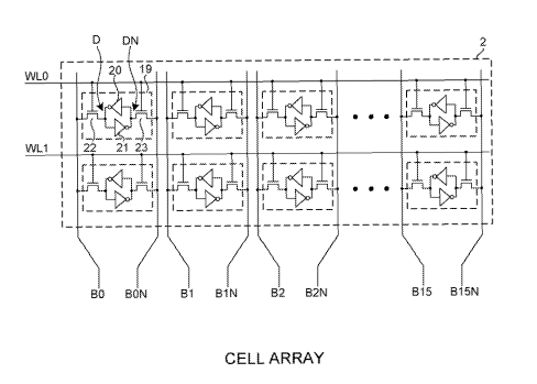
[0016] Figure 2 is a more detailed diagram of memory array 2 of Figure 1.
[0017] Figure 3 is a more detailed diagram of the eight column
multiplexer/demultiplexers 3-10 of Figure 1.
[0018] Figure 4 is a more detailed diagram of the address input latch and
read/write
multiplexer portion of block 11 of Figure 1.
[0019] Figure 5 is a more detailed diagram of the data input latch portion of
block 11 of
Figure 1.
[0020] Figures 6A and 6B are a more detailed diagram of the read clock
generator
circuit 12, the write clock generator circuit 13, the time delayed multiplexer
circuit 14,
the write clock suppressor circuit 16, and the one shot circuit 105 of Figure
1.
[0021] Figure 7 is a waveform diagram that illustrates a first scenario (Case
#1) of an
operation of the pseudo-dual port memory device 1 of Figures 1-6.
[0022] Figure 8 is a waveform diagram that illustrates a second scenario (Case
#2) of an
operation of the pseudo-dual port memory device 1 of Figures 1-6.
[0023] Figure 9 is a waveform diagram that illustrates a second scenario (Case
#3) of an
operation of the pseudo-dual port memory device 1 of Figures 1-6.
CA 02633889 2008-06-10
WO 2007/111709 PCT/US2006/061044
050168
6
[0024] Figure 7A is a simplified waveform diagram of the first scenario (Case
#1).
[0025] Figure 8A is a simplified waveform diagram of the second scenario (Case
#2).
[0026] Figure 9A is a simplified waveform diagram of the third scenario (Case
#3).
[0027] Figure 10 is a simplified waveform diagram of a first example where the
frequency of ACLK is higher than the frequency of BCLK, but BCLK rises at the
same
time that ACLK rises.
[0028] Figure 11 is a simplified waveform diagram of a second example where
BCLK
rises during the time ACLK is low.
[0029] Figure 12 is a simplified waveform diagram of a third example where
BCLK
rises during the time ACLK is high.
DETAILED DESCRIPTION
[0030] Figure 1 is a high-level block diagram of a pseudo-dual port memory
device 1 in
accordance with one embodiment. Memory device 1 includes an array 2 of static
random access memory cells. In the illustrated example, array 2 includes two
rows of
memory cells, where each row includes sixteen memory cells. In addition to
array 2,
memory device 1 includes a set of eight column multiplexer/demultiplexers 3-
10. Only
the first and eighth column multiplexer/demultiplexers 3 and 10 are
illustrated.
Memory device 1 also includes an address input latch, read/write multiplexer,
and data
input latch circuit 11, a read clock generator circuit 12, a write clock
generator circuit
13, a time delayed multiplexer circuit 14, a one shot circuit 15, and a write
clock
suppressor circuit 16. Write clock suppressor circuit 16 includes an
suppressor clock
generator circuit 17 and a suppressor circuit 18. The circuitry in blocks 3-15
is control
circuitry that controls access to array 2.
[0031] Figure 2 is a more detailed diagram of memory array 2. Each of the
memory
cells is a six-transistor memory cell. Reference numeral 19 identifies the
memory cell
in the upper left hand corner of the array. Four of the transistors of memory
cell 19 are
interconnected to form a pair of cross-coupled inverters 20 and 21. A first
data node D
of memory cell 19 is coupled to the output lead of inverter 20 and is coupled
to the input
lead of inverter 21. A second data node DN of memory cell 19 is coupled to the
output
lead of inverter 21 and is coupled to the input lead of inverter 20. A first
access
transistor 22 is provided so that data node D can be selectively coupled to a
vertically
extending bit line BO. A second access transistor 23 is provided so that data
node DN
can be selectively coupled to a vertically extending bit line BON. As
illustrated, pairs of
CA 02633889 2008-06-10
WO 2007/111709 PCT/US2006/061044
050168
7
bit lines BO and BON, B 1 and B IN...B 15 and B 15N extend through the array
in the
vertical dimension. For example, the pair of bit lines BO and BON extends
vertically up
through the leftmost column of memory cells. The "N" suffix in this notation
indicates
"not", or the complement of the signal having the same signal name without the
"N"
suffix. A pair of word lines WLO and WLl extends through the array in the
horizontal
dimension. Word line WLO is coupled to the gates of the access transistors of
the
various memory cells of the upper row of memory cells of the array. Word line
WLl is
coupled to the gates of the access transistors of the various memory cells of
the lower
row of memory cells of the array.
[0032] Figure 3 is a more detailed diagram of the eight column
multiplexer/demultiplexers 3-10 of Figure 1. Each column
multiplexer/demultiplexer
has two pairs of bit line leads. Column multiplexer/demultiplexer 3, for
example, has
leads that are coupled to a first pair of bit lines BO and BON and also has
leads that are
coupled to a second pair of bit lines Bl and BIN. The two pairs of bit lines
are
illustrated extending down from the top into the column
multiplexer/demultiplexer 3 in
Figure 3.
[0033] Each column multiplexer/demultiplexer receives a read column address
RCAO
and its complement RCAON. During a read operation, one of the two pairs of bit
lines
is multiplexed by multiplexer 24 onto a differential pair of input leads of a
sense
amplifier 25. Which one of the two pairs of bit lines is determined by the
values RCAO
and RCAON. Sense amplifier 25 includes a latch that latches the value being
output
onto the data output lead of the column multiplexer/demultiplexer. The latch
is
transparent when an input signal SENS is low and the latch latches on a low-to-
high
transition of the signal SENS. The data output leads DOUT[0:7] of memory
device 1
are the data output leads of the eight column multiplexers/demultiplexers 3-
10,
respectively.
[0034] Each column multiplexer/demultiplexer also receives an internal clock
signal
ICLK. The signal ICLK is a precharge signal that causes the bits lines to be
precharged
when ICLK is low. The ICLK signal is described in further detail below.
[0035] Each column multiplexer/demultiplexer also receives a write column
address
WCAO and its complement WCAON. Each column multiplexer/demultiplexer also
receives a latched data input value and its complement. The first column
multiplexer/demultiplexer 3, for example, receives latched input data value
DIN[0] and
its complement DINN[0]. During a write operation, the input data values DIN[0]
and
CA 02633889 2008-06-10
WO 2007/111709 PCT/US2006/061044
050168
8
DINN[0] are demultiplexed by demultiplexer 26 onto one of the two pairs of bit
lines
that are coupled to the column multiplexer/demultiplexer 3. The particular
pair of bit
lines is determined by the write column address WCAO and its complement WCAON.
Accordingly, during a read operation data passes from a selected pair of the
bit lines,
through multiplexer 24, through the sense amplifier 25, and onto the data
output lead
DOUT[0] of the column multiplexer/demultiplexer 3. During a write operation,
data
passes from the data input leads DIN[0] and DINN[O], through demultiplexer 26,
and
onto a selected pair of the bit lines BO and BON or Bl and BIN.
[0036] Figure 4 is a more detailed diagram of the address input latch and
read/write
multiplexer portion of block 11 of Figure 1. The circuit of Figure 4 latches
an incoming
two-bit read address RADR[1:0] and also latches an incoming two-bit write
address
WADR[1:0]. The circuit of Figure 4 outputs word line values WLl and WLO, read
column address values RCAO and RCAON, and write column address values WCAO and
WCAON.
[0037] Figure 5 is a more detailed diagram of the data input latch portion of
block 11 of
Figure 1. As illustrated, there are eight identical data input latches 27-34
that are
organized in parallel so that they latch an eight-bit input data value
DATAIN[7:0] and
output an eight-bit latched data value DIN[7:0] and its complement DINN[7:0].
A write
clock signal WCLK is used to latch the incoming input data value DATAIN[7:0]
into
the eight data input latches. Each data input latch is transparent when the
write clock
signal WCLK is low, and latches when the write clock signal WCLK transitions
low-to-
high. In data input latch 27, the transistors making up the pass gate 35 and
the cross-
coupled inverters 36 and 37 together form a transparent latch 38. The digital
value
stored in the data input latch as well as the complement of the digital value
stored are
supplied onto the data leads DIN[0] and DINN[0] of the data input latch when
the
read/write decoding clock signal RWDCLK is asserted high. If, on the other
hand, the
signal RWDCLK is low, then both the signals on both the DIN[0] and DINN[0]
output
leads are forced high.
[0038] Figure 6 is a more detailed diagram of the read clock generator circuit
12, the
write clock generator circuit 13, the time delayed multiplexer circuit 14, the
one shot
circuit 15, and the write clock suppressor circuit 16 of Figure 1. The
circuitry of Figure
6 outputs a read clock signal RCLK, a write clock signal WCLK, the internal
clock
signal ICLK, and the read/write decoding clock signal RWDCLK.
CA 02633889 2008-06-10
WO 2007/111709 PCT/US2006/061044
050168
9
[0039] Operation of pseudo-dual port memory device 1 is described below in
connection with the waveforms diagrams of Figures 7-9. Figure 7 is a waveform
diagram of a first scenario (Case #1) in which the rising edges of the input
clock signal
ACLK for the first port and the input clock signal BCLK for the second port
occur
simultaneously. Figure 8 is a waveform diagram of a second scenario (Case #2)
in
which the rising edge of the input clock signal ACLK for the first port
precedes the
rising edge of the input clock signal BCLK for the second port. Figure 9 is a
waveform
diagram of a third scenario (Case #3) in which the rising edge of the input
clock signal
BCLK for the second port precedes the input clock signal ACLK for the first
port.
Signals names preceded in Figures 7-9 with an asterisk are externally supplied
input
signals that are supplied to the pseudo-dual port memory device 1.
[0040] Initially, the clock signal ICLK is low as illustrated in Figure 7.
ICLK is
supplied to the column multiplexer/demultiplexers 3-10 as illustrated in
Figure 3. When
ICLK is low, the P-channel transistors 39-41 and 42-44 in each of the column
multiplexer/demultiplexers are conductive. All the pairs of bit lines are
therefore
precharged to supply voltage VCC. This precharging of the bit lines is an
initial
condition.
[0041] Because a read operation is to be performed, a two-bit read address
RADR[1:0]
is placed on the two read address input leads 45 and 46 of pseudo-dual port
memory 1,
and the read select signal CSAN is asserted on input lead 47 of pseudo-dual
port
memory 1. Because a write operation is also to be performed, a two-bit write
address
WADR[1:0] is placed on the two write address input leads 48 and 49 of pseudo-
dual
port memory 1, and the write select signal CSBN is asserted on input lead 50
of pseudo-
dual port memory 1. The eight-bit data value DATAIN[7:0] that is to be written
during
the write operation is supplied onto the eight data input leads 51-58 of the
pseudo-dual
port memory 1. The read address input leads 45 and 46, a read clock input lead
59, and
the data output leads 60-67 constitute a first port (a read only port) of the
pseudo-dual
port memory device 1. The write address input leads 48 and 49, a write clock
input lead
68, and the data input leads 51-58 constitute a second port (a write only
port) of the
pseudo-dual port memory device 1.
[0042] After the information on input leads 45-58 and 68 has been set up for a
period of
time, the first input clock signal ACLK on input lead 47 and the second input
clock
signal BCLK on input lead 50 transition high simultaneously at time Tl (see
Figure 7).
CA 02633889 2008-06-10
WO 2007/111709 PCT/US2006/061044
050168
When the first input clock signal ACLK transitions high, the value of the read
select
signal CSAN is latched into the latch of the RCLK generator circuit 12 of
Figure 6. If
CSAN is low, then the voltage on latch node 69 is pulled to ground and is
latched by
cross-coupled inverters 70-71. If CSAN is high, then the voltage on node 69
would
have remained in its previously latched state. As the waveform diagram of
Figure 7
shows, CSAN is low in the presently described operational example. A digital
low is
therefore latched onto node 69. A digital high is therefore latched onto node
72. The
digital value on node 72 is the value of the read clock signal RCLK. The read
clock
signal RCLK therefore transitions high as illustrated in Figure 7.
[0043] In a similar fashion, the write clock select signal CSBN is latched
into the latch
of the write clock generator 13 of Figure 6. If CSBN is low, then the voltage
on node
73 is pulled to ground and is latched by cross-coupled inverters 74-75. If
CSBN is high,
then the voltage on node 73 remains in its previously latched state. As the
waveform
diagram of Figure 7 shows, CSBN is low in the presently described operational
example. A digital low is therefore latched onto node 73, and a digital high
is latched
onto node 76. The digital value on node 76 is the value of the write clock
signal
WCLK. The write clock signal WCLK therefore transitions high as illustrated in
Figure
7.
[0044] In the waveform of Figure 7, both ACLK and BCLK were initially digital
lows.
Because ACLK was low, a digital high was present on node 200 in the
suppression
clock generator 17 of Figure 6. P-channel transistor 201 was therefore non-
conductive.
Because BCLK was low, a digital low was present on node 202 in the suppression
clock
generator 17 of Figure 6. N-channel transistor 203 was therefore non-
conductive. Node
204 therefore remained latched to hold it previous digital value. When ACLK
transitions high as illustrated in Figure 7, inverter 205 asserts a digital
low onto node
200, thereby causing P-channel transistor 201 to be conductive and causing N-
channel
transistor 206 to be nonconductive. Node 204 is therefore pulled up to a
digital high.
Cross-coupled inverters 207 and 208 are latched so that the voltage on node
209 is a
digital low. The voltage on node 209 is the suppression clock signal SCLK. As
long as
ACLK is a digital high, the latch of the suppression clock generator 17 is
held in this
state, regardless of the value of BCLK. Note in Figure 7 that the signal SCLK
is a
digital low at time T 1 and remains a digital low thereafter.
CA 02633889 2008-06-10
WO 2007/111709 PCT/US2006/061044
050168
11
[0045] The address input latch of Figure 4 includes a pair of latches 77 and
78 for
latching the two read address bit values RADR[0] and RADR[l], respectively.
Latches
77 and 78 are transparent when signal RCLK is low, and latch on the rising
edge of
RCLK. The value of RADR[0] is therefore latched onto node 79 in latch 77 on
the
rising edge of RCLK. The value of RADR[1] is therefore latched onto node 80 in
latch
78 on the rising edge of RCLK.
[0046] At time Tl in the waveform diagram of Figure 7, RCLK is low and has not
yet
transitioned high. Latch 77 is therefore transparent. RADR[O] is therefore
present on
node 79. Because RCLK is low, NAND gate 81 outputs a digital high. Gating
circuit
82 therefore asserts both RCAO and RCAON high. Because RCAO and RCAON are
high and are driving the P-channel transistors of the write demultiplexers in
the column
multiplexer/demultiplexers of Figure 3, the write demultiplexers are disabled
and the bit
lines are not coupled to the input leads of the sense amplifiers of the column
multiplexer/demultiplexers. The write demultiplexers are disabled because the
operation to be performed next is a read operation.
[0047] At time Tl in the waveform diagram of Figure 7, RCLK is low and latch
78 is
transparent. RADR[1] is therefore present on node 80. Because RWDCLK is a
digital
low as illustrated in Figure 7, the latched value of RADR[ 1] on node 80 (see
Figure 4) is
supplied through multiplexer 83 onto node 84. Because ICLK is low, however,
gating
circuit 85 blocks the signal on node 84 from being output onto the word line
output
leads 86 and 87. Digital low signals are present on the word line output leads
86 and
87. Because the access transistors of the memory cells of Figure 4 are N-
channel
transistors, the low signals on WLO and WLl prevent any of the access
transistors in the
array 2 from being conductive.
[0048] The address input latch of Figure 4 further includes a second pair of
latches 88
and 89 for latching the two write address bit values WADR[0] and WADR[1],
respectively. Latches 88 and 89 are transparent when signal WCLK is low, and
latch on
the rising edge of WCLK. The value of WADR[0] is therefore latched onto node
90 in
latch 88 on the rising edge of WCLK. The value of WADR[1] is therefore latched
onto
node 91 in latch 89 on the rising edge of WCLK.
[0049] At time Tl in the waveform diagram of Figure 7, WCLK is low and has not
yet
transitioned high. Latch 88 is therefore transparent. WADR[0] is therefore
present on
node 90. Because WCLK is low, NAND gate 92 outputs a digital high. Gating
circuit
93 therefore forces both WCAO and WCAON low. Because WCAO and WCAON are
CA 02633889 2008-06-10
WO 2007/111709 PCT/US2006/061044
050168
12
low and are driving the N-channel transistors of the multiplexers in the
column
multiplexer/demultiplexers of Figure 3, the demultiplexers are disabled and
the bit lines
are not coupled to the data input leads DIN[7:0] and DINN[7:0] of the column
multiplexer/demultiplexers.
[0050] At time Tl in the waveform diagram of Figure 7, WCLK is low and latch
89 is
transparent. WADR[1] is therefore present on node 91. Because RWDCLK is a
digital
low as illustrated in Figure 7, the value on node 91 is not supplied through
multiplexer
83 onto node 84.
[0051] At time Tl, ICLK is low. The transistors 39-44 in the column
multiplexer/demultiplexers 3-10 are therefore conductive. The bit lines of
each pair of
bit lines are coupled together, and are coupled to supply voltage VCC. The bit
lines are
therefore said to be precharged.
[0052] Next, the externally supplied first input clock signal ACLK and the
externally
supplied second input clock signal BCLK transition high. The two clock signals
ACLK
and BCLK transition high simultaneously.
[0053] Before the transition of the signal ACLK, the signal ACLK was a digital
low.
CSAN was a digital low as indicated by the waveform of Figure 7. NOR gate 94
of
Figure 6 therefore was supplying a digital high signal onto the gate of N-
channel
transistor 95. When ACLK transitions high, a high signal is present on the
gate of N-
channel transistor 96. Both N-channel transistors 96 and 95 are therefore
conductive for
a short amount of time until the digital high ACLK signal propagates through
inverters
97 and 98 and NOR gate 94 to force the voltage on the gate of N-channel
transistor 95
low. The voltage on node 69 is therefore pulled to ground momentarily through
transistors 96 and 95. The voltage on node 69 is thereby latched to a digital
low and the
voltage on node 72 is latched to a digital high. This is illustrated in the
waveform of
Figure 7 by the low-to-high transition of the signal RCLK.
[0054] A similar event happens in the WCLK generator 13. Before the low-to-
high
transition of the signal BCLK, CSAB was a digital low as indicated by the
waveform of
Figure 7. NOR gate 99 of Figure 6 therefore was supplying a digital high
signal onto
the gate of N-channel transistor 100. When BCLK transitions high, a high
signal is
present on the gate of N-channel transistor 101. Both N-channel transistors
101 and 100
are therefore conductive for a short amount of time until the digital high
BCLK signal
propagates through inverters 102 and 103 and NOR gate 99 to force the voltage
on the
gate of N-channel transistor 100 low. The voltage on node 73 is therefore
pulled to
CA 02633889 2008-06-10
WO 2007/111709 PCT/US2006/061044
050168
13
ground momentarily through transistors 101 and 100. The voltage on node 73 is
thereby latched to a digital low and the voltage on node 76 is latched to a
digital high.
This is illustrated in the waveform of Figure 7 by the low-to-high transition
of the signal
WCLK.
[0055] When RCLK transitions high, latches 77 and 78 of Figure 4 latch the
read
address values RADR[0] and RADR[1] onto nodes 79 and 80, respectively. This is
illustrated in the waveform labeled LATCHED AADR[1:0] in Figure 7 by the
vertical
dashed line. Because RCLK is high and RWDCLK is low, NAND gate 81 outputs a
digital low signal. Gating circuit 82 therefore does not force both RCAO and
RCAON
high as before. The latched RADR[0] value on node 79 is output as RCAO and its
complement is output as RCAON. The read column address values are supplied to
the
column multiplexer/demultiplexers 3-10 in preparation for the upcoming read
operation.
This is represented in Figure 7 by the waveform labeled COLUMN ADR TO COL
MUX. As seen in Figure 3, the read column addresses RCAO and RCAON cause read
multiplexer 24 to select one of the pairs of bit lines and to couple the
selected pair to the
input leads of sense amplifier 25.
[0056] When WCLK transitions high, latches 88 and 89 of Figure 4 latch the
write
address values WADR[0] and WADR[1] onto nodes 90 and 91, respectively. This is
illustrated in the waveform labeled LATCHED BADR[1:0] in Figure 7 by the
vertical
dashed line. Because signal RWDCLK is a digital low, however, NAND gate 92 of
Figure 4 continues to output a digital high, and gating circuit 93 continues
to force both
write column address values WCAO and WCAON low to their inactive states. The
WADR[1] address value that is latched onto node 91 is blocked from being
output onto
the word line WL because RWDCLK is a digital low and is selecting the upper
input
lead of multiplexer 83.
[0057] Returning to Figure 6, the high-to-low transition on node 69 is
supplied onto the
lower input lead of NAND gate 104. NAND gate 104 therefore asserts the
internal
clock signal ICLK high. This is represented in Figure 7 by the low-to-high
transition of
signal ICLK. When ICLK transitions high, the precharging of the bit lines of
array 2 is
stopped. Precharging transistors 39-44 of Figure 3 become nonconductive in
preparation for the upcoming read operation.
[0058] When ICLK transitions high, gating circuit 85 of Figure 4 no longer
forces
digital logic level low signals onto both of the word lines. The latched read
address
value RADR[1] on node 80 is therefore output onto word line WLl output lead
86. The
CA 02633889 2008-06-10
WO 2007/111709 PCT/US2006/061044
050168
14
complement of the read address value is output onto word line WLO output lead
87. A
digital high is therefore present on one of the word lines WLO and WLl. This
is
represented in the waveform of Figure 7 by the low-to-high transitioning of
the
waveform labeled WL (ONE OF WLO and WLl). As seen in Figure 2, the high value
on a word line causes all the access transistors of all the memory cells of
the associated
row of sixteen memory cells to be conductive. One entire sixteen-bit value is
output
from the array 2 to the eight column multiplexer/demultiplexers. The eight
column
multiplexers 3-10 select one eight-bit value to be output onto the data output
leads of
the memory based on the value of the read address values RCAO and RCAON. The
differential voltages on selected pairs of bit lines are coupled through the
multiplexers
of the column multiplexer/demultiplexers, and onto the input leads of the
sense
amplifiers of the column multiplexer/demultiplexers. The resulting eight-bit
value is
output onto the output leads 60-67 of the memory device 1. The outputting of
the eight-
bit data value is illustrated in Figure 7 at time T2 in the waveform labeled
DOUT[7:0](READ).
[0059] Returning to Figure 6, a one shot circuit 105 detects the low-to-high
transition of
the signal ICLK. After a delay, one shot circuit 105 outputs a high pulse of a
RESET
signal. This is illustrated in Figure 7 by the first high pulse in the
waveform labeled
RESET. In Figure 7, the dashed arrow labeled A represents the delay introduced
by one
shot circuit 105.
[0060] RESET pulsing high causes RCLK to transition low because the high value
of
RESET is present on the upper input lead of NAND gate 106 of Figure 6. RDWCLK
is
a digital low, so a digital high is also present on the lower input lead of
NAND gate 106.
NAND gate 106 therefore outputs a digital low signal, thereby causing P-
channel
transistor 107 to be made conductive. Node 69 is pulled high because node 69
is
coupled to VCC through transistor 107. The signal RCLK on node 72 therefore
transitions low. This is illustrated in Figure 7 by the high-to-low transition
of the RCLK
waveform. It is therefore seen that the time delayed multiplexer 14 and the
one shot
circuit 105 operate together to clear the RCLK signal low at the end of the
read
operation.
[0061] A digital high is present on the upper input lead of NAND gate 104 in
Figure 6.
ICLK is therefore low. When the voltage on node 86 transitions high, a digital
high
signal is also present on the lower input lead of NAND gate 104. NAND gate 104
therefore outputs a digital low signal. This is illustrated in Figure 7 by the
high-to-low
CA 02633889 2008-06-10
WO 2007/111709 PCT/US2006/061044
050168
transition of the signal ICLK. The precharging transistors 39-44 in the column
multiplexer/demultiplexers are therefore made conductive again to start a
precharging
operation for the upcoming write operation.
[0062] Before the data being output from the memory device can change due to
the
precharging, a sense signal SENS is supplied to the latched in the sense
amplifiers in the
column multiplexer/demultiplexers. The low-to-high transition of the signal
SENS
causes the latches in the column multiplexer/demultiplexers to latch and hold
the data
values that is being read out on the output leads 60-67 of the memory device
1. A one
shot circuit (not shown) generates the SENS signal and pulses the SENS signal
high
upon the falling edge of the signal ICLK when RWDCLK is low. The latching of
the
output data is considered the end of the read operation.
[0063] RCLK transitioning low when WCLK is a digital high causes a digital low
signal to be present on both input leads of NOR gate 108 in the time delayed
multiplexer 14 of Figure 6. NOR gate 108 therefore outputs a digital high
signal. This
signal propagates through inverters 109 and 110. RWDCLK therefore transitions
high
as illustrated in Figure 7 by the low-to-high transition in the waveform
labeled
RWDCLK.
[0064] Returning to Figure 4, the low-to-high transition in the signal RWDCLK
causes
the write address values to be output from the address input latch of Figure
4.
RWDCLK being high causes a digital low to be present on the upper input lead
of
NAND gate 81. NAND gate 81 therefore outputs a digital high. This causes
gating
circuit 82 to force RCAO and RCAON to digital high values. Forcing both RCAO
and
RCAON high causes the read multiplexer 24 in the column
multiplexer/demultiplexers
of Figure 3 to couple no bit lines to the sense amplifiers.
[0065] Returning to Figure 4, RWDCLK being high causes NAND gate 92 to output
a
digital high signal. Gating circuit 93 therefore no longer blocks the write
address value
WADR[0] latched in latch 88 from being output onto WCAO and WCAON. The write
column address value WADR[0] is therefore communicated through gating circuit
93 to
the write demultiplexer 26 in the column multiplexer/demultiplexer of Figure
3. The
data input values on DIN[7:0] and DINN[7:0] are therefore communicated through
the
write demultiplexers of the column multiplexer/demultiplexers onto a selected
set of
eight pairs of bit lines. Which set of eight pairs is selected is determined
by the values
of WCAO and WCAON. In Figure 3, the data values are communicated through the
CA 02633889 2008-06-10
WO 2007/111709 PCT/US2006/061044
050168
16
write demultiplexer and up into the memory array 2 so that the data values can
be
written into the row of memory cells identified by word line address values
WLO and
WLl.
[0066] Returning to Figure 6, the low-to-high transition of RWDCLK continues
to
propagate through inverters 111 and 112 and onto the upper input lead of NAND
gate
113. Because SCLK has been a digital low, inverter 210 in the suppressor
circuit 18 has
been outputting a digital high onto the lower input lead of NAND gate 211.
Because
WCLK is a digital high, NAND gate 211 outputs a digital low, and inverter 212
asserts
the signal SWCLK high. Accordingly, when SCLK is low, the write clock WCLK is
gated through suppressor circuit 18 and is output as SWCLK.
[0067] Because the digital high signal SWCLK has been present on the lower
input lead
of NAND gate 113 in the time delayed multiplexer 14, the low-to-high
transition on the
upper input lead of NAND gate 113 causes NAND gate 113 to output a digital low
signal, which is inverted by inverter 114. A digital high signal is therefore
asserted onto
the upper input lead of NAND gate 115. A digital high signal was already
present on
the lower input lead of NAND gate 115 due to the low value of the signal RESET
causing NAND gate 116 of the WCLK generator circuit 13 to output a digital
high
signal. NAND gate 115 therefore outputs a digital low signal, thereby causing
NAND
gate 104 to assert ICLK high. This propagation delay from the rising edge of
RWDCLK to the rising edge of ICLK is shown in Figure 7 by the dashed arrow
labeled
B. The rising edge of the signal ICLK terminates the precharge of the write
operation.
[0068] Returning to Figure 4, the rising edge of ICLK is supplied to gating
circuit 85.
Gating circuit 85 therefore no longer forces both WLO and WLl to be low, but
rather
allows the write address value WADR[1] on node 84 to be output onto word line
WLl
output lead 86. The write address value that was latched into node 91 is
multiplexed
onto node 84 due to the value of RWDCLK being a digital high during the write
operation. The result is that the write address value WADR[1] is output onto
WLl
output lead 86 and its complement is output onto WLO output lead 87. This is
illustrated in Figure 7 by the transitioning in the waveform labeled WL (ONE
OF WLO
AND WLl).
[0069] The write address values WADR[0] and WADR[1] are therefore used to
address
memory array 2 during the write operation. This is represented in Figure 7 by
the label
WCA that appears in the waveform labeled COLUMN ADR TO COL MUX. Data in
the eight addressed memory cells may switch at time T3 as illustrated in
Figure 7.
CA 02633889 2008-06-10
WO 2007/111709 PCT/US2006/061044
050168
17
[0070] Returning to Figure 6, the low-to-high transitioning of ICLK is again
detected
by one shot circuit 105. After a delay represented in Figure 7 by the dashed
arrow
labeled C, one shot circuit 105 outputs a high pulse of the signal RESET. The
high
pulse of the signal RESET is asserted onto the upper input lead of NAND gate
116.
Because RWDCLK is now high, there are digital high signals on both input leads
of
NAND gate 116. NAND gate 116 drives a digital low signal onto the gate of P-
channel
transistor 117, thereby latching a digital high signal onto node 73 in the
WCLK
generator circuit 13. Signal WCLK on node 76 therefore transitions low. This
is
illustrated in Figure 7 by the high-to-low transition of the waveform WCLK.
The time
delayed multiplexer 14 and one shot circuit 105 therefore together cause the
resetting of
the signal WCLK low at the end of the write operation.
[0071] WCLK transitioning low causes NAND gate 211 in suppressor circuit 18 to
output a digital high. Inverter 212 therefore forces SWCLK low. WCLK is
therefore
gated through suppressor circuit 18 because the suppression signal SCLK is
low.
[0072] SWCLK transitioning low causes NAND gate 113 in time delayed
multiplexer
14 to output a digital high. Inverter 114 outputs a digital low thereby
causing NAND
gate 115 to output a digital high. Because RCLK is a digital low, the voltage
on node
69 in the RCLK generator circuit 12 is a digital high. There are digital high
signals on
both input leads of NAND gate 104, thereby causing NAND gate 104 to assert
ICLK
low. This is illustrated in Figure 7 by the second high-to-low transition of
the signal
ICLK.
[0073] SWCLK transitioning low also causes a digital high signal to be present
on the
lower input lead of NOR gate 108 of Figure 6. NOR gate 108 outputs a digital
low
signal that propagates through inverters 109 and 110, thereby causing RWDCLK
to
transition low at the end of the write operation. This is illustrated in
Figure 7 by the
high-to-low transition in the waveform labeled RWDCLK. At this point,
precharging of
the bit lines of memory array 2 is initiated in preparation for a subsequent
memory
access operation.
[0074] It is therefore recognized that pseudo-dual port memory device 1
performs a
read operation followed by a write operation. The end of the read operation
and the
beginning of the write operation are not dependent on the falling edge of an
input clock
signal. Rather, asynchronous propagation delays through logic circuitry and a
one shot
circuit are used to time the control signals necessary to carry out the first
read operation,
to precharge the bit lines of the memory for a second operation, and to carry
out the
CA 02633889 2008-06-10
WO 2007/111709 PCT/US2006/061044
050168
18
second write operation. The amounts of time of delay A, delay B, and delay C
can be
increased or decreased during the design of a memory device in order to change
the
relative amount of time that is allotted for the read operation versus the
write operation.
[0075] Figure 7A is a simplified waveform diagram for case #1. The rising
edges of
ACLK and BCLK coincide. SCLK remains low and never transitions high. The
suppressor circuit 18 of Figure 6 therefore always passes the value of WCLK
through to
be the value of SWCLK. The signal SWCLK is supplied to the time delayed
multiplexer 14 in the place of WCLK. The time delayed multiplexer 14 therefore
receives RCLK and SWCLK (which has the same timing as WCLK), and generates the
time delayed signal RWDCLK so as to perform the read operation followed by the
write
operation.
[0076] In the above-described scenario, there is both a read operation and a
write
operation to be performed. In a scenario in which only a read operation is to
be
performed, then RCLK would be latched high, RWDCLK would be forced low for the
read operation, one shot circuit 105 would then clear RCLK low, but WCLK would
not
have been latched high. Consequently, RWDCLK would not be forced high at the
end
of the read operation, and there would be no second write operation.
[0077] Similarly, in a scenario in which only a write operation is to be
performed, then
WCLK would be latched high but RCLK would not be latched high. RWDCLK would
therefore be forced high for a write operation, one shot circuit 105 would
then reset
WCLK low at the end of the read operation, but there would be no second memory
operation.
[0078] Consider a situation in which WCLK were latched high when RCLK had not
yet
been latched high. Time delayed multiplexer 14 would assert RWDCLK high for a
write operation and the write operation would be initiated as described above
in a
condition wherein a write operation is to be performed but no read operation
is to be
performed. If RCLK were then latched high (as in case #3) due to an attempted
read
from the first port, then NOR gate 108 in time delayed multiplexer 14 would
output a
digital low, the low signal would propagate through inverters 109 and 110, and
RWDCLK would be asserted low. Asserting RWDCLK low before completion of the
write operation, however, may cause a malfunction of the pseudo-dual port
memory.
The suppression clock generator 17 and the suppressor circuit 18 prevent such
a
situation by suppressing assertion of WCLK high as it is presented to time
delayed
multiplexer 14 (WCLK is presented to time delayed multiplexer 14 as SWCLK)
until
CA 02633889 2008-06-10
WO 2007/111709 PCT/US2006/061044
050168
19
the RCLK signal has transitioned high. Suppression of WCLK in this manner
prevents
the malfunction that would otherwise have occurred if RCLK were asserted
shortly after
a write operation had been initiated.
[0079] Figure 8 is a waveform diagram that illustrates an operation of pseudo-
dual port
memory 1 in case #2. In case #2, the first input clock signal ACLK that is
supplied to
the first port of the memory is asserted high first at time TIA. The values of
CSAN and
AADR[1:0] are therefore latched into the memory shortly after time TIA. The
second
input clock signal BCLK that is supplied to the second port of the memory is
asserted
some time later at time TIB. The values of CSBN and BADR[1:0] and DATAIN[7:0]
are therefore latched into the memory shortly after time T I B.
[0080] Because the read operation is to occur before the write operation, the
earlier
rising ACLK causes RCLK to be asserted. RCLK in turn initiates the read
operation
before the rising edge of BCLK. When the read operation is completed as
determined
by propagation delay A and the subsequent falling edge of RCLK, the time
delayed
multiplexer 14 of Figure 6 asserts RWDCLK to initiate the write operation. The
write
clock signal WCLK, which at that time has been asserted, is gated through
suppressor
circuit 18 and is supplied to time delayed multiplexer 14 in the form of
SWCLK. When
the read operation is completed, the time delayed multiplexer 14 is therefore
able to
initiate the write operation.
[0081] Figure 8A is a simplified waveform diagram for case #2. The rising edge
of
ACLK precedes the rising edge of BCLK. SCLK remains low and never transitions
high. The suppressor circuit 18 of Figure 6 therefore never suppresses WCLK.
WCLK
is gated through suppressor circuit 18 and is supplied to time delayed
multiplexer 14 as
SWCLK. Because the write signal SWCLK is present at the time delayed
multiplexer
14 at the time when the read operation is completed, time delayed multiplexer
14 is able
to initiate the write operation in the same way as in case #1.
[0082] Figure 9 is a waveform diagram that illustrates an operation of pseudo-
dual port
memory 1 in case #3. In case #3, the second input clock signal BCLK that is
supplied
to the second port of the memory is asserted first at time TIB. The values of
CSBN and
BADR[1:0] and DATAIN[7:0] for the write operation are therefore latched into
the
memory shortly after time TIB. The first input clock signal ACLK that is
supplied to
the first port of the memory is asserted some time later at time TIA. The
values of
CA 02633889 2008-06-10
WO 2007/111709 PCT/US2006/061044
050168
CSAN and AADR[1:0] for the read operation are therefore latched into the
memory
shortly after time T I A.
[0083] Because the write operation is to occur after the read operation, the
earlier rising
BCLK cannot be allowed to assert SWCLK high so that the write operation is
initiated.
The suppression clock SCLK is therefore asserted high during an initial period
(roughly
between time TIB and time TIA) until the read clock ACLK transitions high.
During
this initial period, SCLK suppresses the write clock that is being supplied to
the time
delayed multiplexer 14 (the write clock WCLK is supplied to time delayed
multiplexer
14 as SWCLK). Suppressing SWCLK during this initial period prevents the time
delayed multiplexer 14 from initiating the write operation before the read
operation.
[0084] Generation of the suppression clock SCLK is explained in connection
with
Figure 6. ACLK at this time is low. Inverter 205 therefore outputs a digital
high onto
node 200. P-channel transistor 201 is therefore non-conductive and N-channel
transistor 206 is conductive. BCLK is initially low, and then transitions
high. Inverters
213-215 therefore initially output a digital high onto the gate of N-channel
transistor
216. Transistor 216 is therefore initially conductive but node 204 is not
coupled to
ground because N-channel transistor 203 is nonconductive. When BCLK
transitions
high, the voltage on node 202 transitions high thereby making N-channel
transistor 203
conductive. It takes time, however, for the high signal on node 202 to
propagate
through inverters 213-215 to force the gate of N-channel transistor 216 low
and turn
transistor 216 off. Therefore, for a short period of time after the rising
edge of BCLK,
all three N-channel pulldown transistors 203, 216 and 206 are conductive and
node 204
is momentarily coupled to ground potential. The momentary coupling to ground
potential latches a digital low onto node 204. The suppression clock SCLK on
node 209
is therefore asserted high. This illustrated in Figure 9 by the rising edge of
the
waveform labeled SCLK.
[0085] Even through WCLK rises shortly after time TIB, the high value of
suppression
clock SCLK suppresses the write clock signal SWCLK supplied to the time
delayed
multiplexer 14. This condition persists until the input clock signal ACLK for
the read
port transitions high. When ACLK transitions high, inverter 205 outputs a
digital low
onto node 200. P-channel pullup transistor 201 is made conductive, and node
204 is
latched and held high. SCLK is therefore latched and held low, thereby ending
the
initial period of time that the suppression clock SCLK is asserted. The rising
edges of
CA 02633889 2008-06-10
WO 2007/111709 PCT/US2006/061044
050168
21
RCLK and SWCLK are therefore presented to time delayed multiplexer 14 at
substantially the same time.
[0086] Figure 9A is a simplified waveform diagram for case #3. The rising edge
of
BCLK precedes the rising edge of ACLK. The rising edge of BCLK when ACLK is
low causes the latch in the suppression clock generator 17 of Figure 6 to
latch a digital
low onto node 204, thereby latching suppression clock signal SCLK high. The
suppressor circuit 18 of Figure 6 therefore suppresses SWCLK and keeps SWCLK
low
during the time SCLK is high. When ACLK transitions high, a digital high is
latched
onto node 204 in the suppression clock generator 17, thereby latching SCLK
low.
SWCLK is therefore no longer held low by suppressor circuit 18. The value of
the
write clock WCLK is the value of SWCLK for the remainder of the read and write
operations. The time delayed multiplexer 14 and one shot 105 initiate the read
operation and then the write operation as in cases #1 and #2.
[0087] Figure 10 is a simplified waveform diagram illustrating an operation of
pseudo-
dual port memory 1 in a situation in which ACLK has a higher frequency than
BCLK.
The first rising edge of ACLK occurs at the same time as the first rising edge
of BCLK.
This is the situation of Figure 7. The first write operation follows the first
read
operation. In the scenario of Figure 10, there is no rising edge of BCLK
around the
time of the second rising edge of ACLK. The second rising edge of BCLK in
Figure 10
therefore gives rise to a second read operation. In the example, the third
rising edge of
ACLK occurs at the same time as the second rising edge of BCLK. This is the
condition of Figure 7. The second write operation therefore follows the third
read
operation.
[0088] Figure 11 is a simplified waveform diagram illustrating an operation of
pseudo-
dual port memory 1 in a situation in which a rising edge of BCLK occurs at an
earlier
time during the low portion of ACLK. The rising edge of BCLK causes SCLK to be
asserted, thereby suppressing SWCLK until the third rising edge of ACLK. The
write
operation is therefore delayed until after the third read operation.
[0089] Figure 12 is a simplified waveform diagram illustrating an operation of
pseudo-
dual port memory 1 in a situation in which a rising edge of BCLK occurs more
than
three gate delays before the falling edge of ACLK. BCLK therefore rises during
the
time ACLK is high. In this situation, ACLK is high and is holding node 204
pulled up
to VCC when the rising edge of BCLK attempts to momentarily pull node 204 to
CA 02633889 2008-06-10
WO 2007/111709 PCT/US2006/061044
050168
22
ground. Because N-channel transistor 206 is nonconductive, node 204 is not
pulled to
ground and SCLK is not latched high. SWCLK is therefore not suppressed during
an
initial period. SWCLK is therefore illustrated going high shortly after BCLK
transitions
high. This causes a write operation to occur immediately following the second
read
operation. The second read operation in the waveform of Figure 12 is the read
operation due to the second rising edge of ACLK.
[0090] The amounts of time of delay A, delay B, and delay C can be increased
or
decreased during the design of a memory device in order to change the relative
proportion of time that is allotted for the read operation versus the write
operation. The
end of the read operation can overlap the beginning of the write operation in
time. In
some implementations of a memory device, the read operation may be allotted
more
time than the write operation. In other implementations, the write operation
may be
allotted more time than the read operation. Problems associated with
initiating the write
operation using the falling edge of an external clock signal where the falling
edge has an
undesirably large amount of jitter are avoided because the falling edge of an
externally
supplied clock signal is not used to terminate the first read operation and/or
to initiate
the second write operation.
[0091] Although certain specific embodiments are described above for
instructional
purposes, the present invention is not limited thereto. The control circuitry
of the
pseudo-dual port memory can be used in embodiments where the first memory
access
operation is a write operation and the second memory access operation is a
read
operation, where the first memory access operation is a write operation and
the second
memory access operation is a write operation, and where the first memory
access
operation is a read operation and the second memory access operation is a read
operation. Accordingly, various modifications, adaptations, and combinations
of the
various features of the described specific embodiments can be practiced
without
departing from the scope of the invention as set forth in the claims.