Note: Descriptions are shown in the official language in which they were submitted.
CA 02634027 2008-06-12
WO 2007/075444 PCT/US2006/047959
SUB-MICRON SURFACE PLASMON
RESONANCE SENSOR SYSTEMS
CROSS-REFERENCE TO RELATED APPPLICATION
This application claims priority to co-pending provisional application No.
60/750,872, filed on December 16, 2005, entitled "Sub-micron Cavity Surface
Plasmon Sensors and Their Micro-fluidic Applications", the entire disclosure
of
which is incorporated by reference herein.
GOVERNMENTAL INTEREST
Part of the work during the development of this invention was made with
government support from the National Science Foundation under grant number
IBM-0083653 and from NASA under grant number NAG2-1619. Pursuant to
these grants, the U.S. Government has certain rights in the invention
disclosed
herein.
BACKGROUND
A significant trend in medicine is the introduction of point of care (POC)
devices for rapid, bedside diagnosis. These devices enable rapid diagnosis by
first responders or medical staff for time-critical diagnoses, such as for
indicating whether patients are presenting with cardiac symptoms. Tests have
been developed for other indications, such as infectious diseases, drugs of
abuse, cerebrovascular disease, that are intended to circumvent the lengthy
processing hours and high costs accompanying conventional in-house
laboratory assays. Current POC devices are single use only. While this is
suitable for many applications, there is an unmet need for continuous
monitoring devices.
An initial clinical need is a device that can monitor and detect the
presence of infections in intensive care patients. Currently, many intensive
care patients develop infections that are not detected quickly, often leading
to
1
CA 02634027 2008-06-12
WO 2007/075444 PCT/US2006/047959
sepsis or shock and resulting in a large mortality rate. There is a
significant
need for a device that can continuously track the concentration of specific
protein markers in a patient's bloodstream that are indicative of an
infection, for
instance.
Devices that are capable of detecting the presence of selected
chemicals or biological substances include biosensors that interact directly
with
a sample molecule to provide a signal identifying the test molecule.
Biosensors
are often functionalized chemically to make them selective. The readout can
be electrochemical, as is often the case for small molecules (e.g. glucose),
or
can utilize fluorescence or other optical techniques for molecuies such as
proteins or DNA. Typical biosensors can often operate in a continuous reading
mode or can be used multiple times, which differs from conventional laboratory
assays requiring bulk reagent handling, usually yielding only a one-time test
result.
The miniaturization possibilities afforded by biosensors compared to
conventional laboratory assays suggests that point of care (POC) tests could
provide dramatically enhanced diagnostic capabilities. The benefits of POC
testing include: rapid turnaround which aids therapeutic decisions; quick
dissemination of test results to patients, thereby reducing physician workload
and increasing patient satisfaction; reduced paper work and simplified sample
tracking; and reduced need for sp'ecialized technicians. POC tests
administered as panels provide further significant benefits. For example,
screening for several cardiac markers simultaneously saves time and provides
useful additional data. Screens for various types of influenza would aid
diagnosis compared to more limited tests on only single strains.
Emerging applications of biosensors include food and water testing,
drugs of abuse, bio-defense and "white powder" detection, and veterinary
testing, to name a few. Some of these applications have unique needs such
as the need for ultra-fast response time in conjunction with bio-defense
measures, or high sensitivity necessary in food or water testing to detect a
very
low number of E. Coli colony-forming units. Typical water testing products use
reagents that must be incubated in flasks for 18 - 24 hours or longer,
changing
CA 02634027 2008-06-12
WO 2007/075444 PCT/US2006/047959
color to indicate pathogen presence. While these products are very effective,
the lengthy, 24 hour incubation time can be problematic. When the
contaminated water is in a public drinking supply, the water may be in use for
extended periods before a pathogen problem is detected. A product that
continuously monitors water quality can provide a warning within minutes of
actual contamination.
Bio-defense presents unique issues as governmental and military
agencies search for ways to rapidly and interactively detect anthrax,
botulism,
malaria, Ebola virus, ricin, and other potential terrorist agents. Expensive
test
kits are currently used by the US Postal Service that incorporate real-time
PCR
to amplify and analyze crude samples obtained from air or suspicious "white
powder" on packages and envelopes.
A new breed of biosensors utilizes a phenomenon arising from the
interaction of light with a metal surface. This phenomenon is called "surFace
plasmon resonance" and embodies a charge-density (electron cloud) oscillation
that may exist at the interFace of two media with different dielectric
constants or
dielectric constants of opposite signs. This condition is usually met at the
interface between a dielectric (glass) and a metal (typically gold or silver).
The
charge density wave (the electron cloud) is associated with an electromagnetic
wave (the incoming photons), and this coupling reaches a maxima at the
interface and decays exponentially into both media. This coupling is, in
effect,
a surface bound plasma wave (SPW).
This coupling cannot be excited directly by incident optical photons at a
planar metal-dielectric interface because the propagation constant of an SPW
is always higher than that of the wave propagating in the dielectric.
Therefore
to enhance this coupling, attenuated total reflection (ATR), prism couplers
and
optical waveguides, or diffraction at the surface of diffraction gratings is
used.
As the excitation of SPWs by optical photons results in resonant transfer of
energy into the SPW, surface plasmon resonance (SPR) manifests itself by
resonant absorption of the energy of the optical photons_ Owing to the strong
concentration of the electromagnetic field in the dielectric (an order of
magnitude higher than that in typical evanescent field sensors using
dielectric
~
CA 02634027 2008-06-12
WO 2007/075444 PCT/US2006/047959
waveguides) the propagation constant of the SPW, and consequently the SPR
formation, is very sensitive to variations in the optical properties of the
dielectric
adjacent to the metal layer supporting SPW, namely the refractive index of the
dielectric media which may be determined by optically interrogating the SPR.
The thickness of the region of sensitivity varies with the wavelength off the
applied energy, but is typically about 500 nm for wavelengths in the visible
light
range. The refractive index is modified by the presence of materials or
impurities at the surface. This is the fundamental effect that can be used to
identify the materials or impurities with great precision.
Metals are materials that can provide the negative sign dielectric
constant. They have a resonant mode at which the constituent electrons
resonate when excited by electromagnetic radiation having the right
wavelength. Gold, in particular, has a spectrum with a resonance at visible
wavelengths around 510 nm. In the case of the attenuated total reflection in
prism couplers, the evanescent wave is sensitive to the metal surface in
contact with the media within approximately 200 - 400 nm of the surface,
enhanced by the presence of a surface plasmon wave. Such material
effectively modifies the index of refraction and thus the precise angle of
critical
attenuated total reflection. Interactions between a bound substrate and a
sample can thus be probed, measuring small variations in the reflection angle
at maximum SPR production.
This effect can be harnessed to study binding between molecules, such
as between proteins, RNA and/or DNA, or between proteins and viruses or
bacteria. For example, a surface functionalized with a specific antibody will
probe for only one antigen (e.g. antigen A) and discriminate specific binding
from non-specific binding. That is, antigen A will be detected but weaker
interactions between the funct'ionafized protein bound to the surface and
another antigen, say antigen B, can be distinguished. Typically, angular
resolution of a few millidegrees is required to discriminate between selective
and non-selective binding. Thus the detection of protein A in solution as
dilute
as 1pg/mi may be achieved. In addition, the reaction kinetics of the binding
between the surface protein and antigen A can be elucidated.
4
CA 02634027 2008-06-12
WO 2007/075444 PCT/US2006/047959
Most commercial SPR instruments comprise a sample introduction
device or sensor that includes a semispherical dielectric prism coated with a
thin layer (50 nm) of a noble metal such as Au or Ag. This metal coating in
turn
is coated with molecules that will specifically bind a tarqet analyte. These
commercial devices further comprise a light source on a goniometric mount, an
array detector, and various collimation and filtering optics, as depicted
generally in FIG. 1.
Using a semispherical prism, the angle of incidence at the dielectric/air
interface is the same as at the first air/dielectric interface where the ray
from
the light source enters the prism. At the precise incidence angle at which
light
couples to a non-radiative evanescent wave (surface plasmon) in the metal
film, the reflectivity of the film decreases roughly 90% creating an
evanescent
plasmon field which is localized at the metal surface away from the glass. The
evanescent wave's properties depend on the properties of the medium (e.g.,
biomolecules) in contact with the free metal surface of the sensor. Subtle
changes in the refractive index of the medium, such as those associated with
molecular absorption onto the surface, induce detectable changes in the
surface plasmon resonance angle (D. The SPR instrument then adjusts the
detector position to find this new angle and thus measures the change in SPR
angle.
These types of SPR devices have a number of inherent limitations
involving sensitivity, sample size, complexity, and cost. Existing commercial
instruments require large, complex, and delicate moving parts in order to
optimize the incident beam and detector positions_ For instance, the
goniometric mount for the light source is relatively big and heavy, but
delicate.
Moreover, the light source itself must provide polarized light. Typical
sensitivity
limits are on the order of 10-6 refractive index units which is usually
sufficient to
detect targets with a concentration of 1 pg/mmZ of adsorbed molecule and a
size of at least 200 Da, but is not sensitive enough to provide useful
detection
for bio-terrorism agents in concentrations of 0.01 parts per billion as
required by
certain government standards. The typical planar sensor footprint is in the
range of a few mm2 (1/16Ih mmz in the Biacore Flexichip and 2.2 mm2 in the
CA 02634027 2008-06-12
WO 2007/075444 PCT/US2006/047959
Biacore 3000) which creates a technical constraint on the ability to
miniaturize
these sensors. A larger sensor area means that more test fluid must be
provided to flow over the planar sensor. Moreover, the constraints on accuracy
also require more test fluid to provide sufficient molecules or microparticles
to
be detected. Because of an SPR sensor's macroscopic size, arrays of sensing
elements for multiplexed analysis require sample volumes too large for most
technologies used for analytical integration. All of these limitations of
conventional planar sensors reduce the throughput capability of the sensors.
Additionally, most current SPR sensors require p-polarized light (i.e., the
electric vector component is parallel to the plane of incidence) and precise
alignment of their optical parts, which are comparable in complexity to those
of
a tabletop spectrometer. This results in high cost, typically on the order of
several hundred thousand dollars.
6
CA 02634027 2008-06-12
WO 2007/075444 PCT/US2006/047959
DESCRIPTION OF THE FIGURES
FIG. 1 is a schematic representation of the operation of a flat-substrate
SPR sensor of the prior art.
FIG. 2 is an enlarged schematic representation of an SPR sensor in
accordance with one embodiment of the present invention,
FIG. 3 is an electron-microscopic image of an SPR bead sensor
fabricated according to the present invention.
FIG. 4 is a schematic view of a micro-fluidic chip utilizing the SPR
sensor according to the present invention.
FIG. 5 is a schematic representation of an experimental set-up for
evaluating the performance of an SPR sensor according to the present
invention.
FIGS. 6a and 6b are graphs of the spectral performance of the SPR
sensor in the experimental set-up shown in FIG. 5.
FIGS. 7a and 7b are graphs of the spectral performance of the SPR
sensor of the present invention under further experimental conditions.
FIG. 8 is a schematic representation of a micro-fluidic SPR sensor
according to a further embodiment of the invention.
FIG. 9 is a diagram of the sulfo-DSP reaction with the gold layer of the
SPR sensors of the present invention for functionalization of the SPR sensors.
FIGS. 10a and 10b are diagrams of the functionalization reactions using
Carbodiimide coupling reagents.
FIG. 11 is a diagram of micro-fluidic components mounted on a micro-
fluidic SPR sensor of the present invention.
FIG. 12 is a diagram of a micro.-fiuidic SPR sensor of the present
invention with micro-fluidic filtering and pre-concentration modules.
FIG. 13 is a diagram of a micro-fluidic SPR sensor of the present
invention with mapped functionalization for detecting multiple molecules,
ligands or analytes.
7
CA 02634027 2008-06-12
WO 2007/075444 PCT/US2006/047959
FIG. 14 is a diagram of the components of a micro-fluidics SPR sensor
system in accordance with the present invention.
FIG. 15 is a schematic representation of a sensor according to the
present invention that is capable of simultaneously evaluating multiple
chemicals.
8
CA 02634027 2008-06-12
WO 2007/075444 PCT/US2006/047959
SUMMARY OF THE INVENTION
Evanescent-wave sensors using SPR techniques for biomolecular
interaction analysis, for instance, provide several advantages, including non-
intrusiveness, real-time monitoring of the binding of target analytes, ligands
or
molecules and label-free conditions. A mechanism to increase the sensitivity
of
SPR sensors while reducing the size of the sensor would be very desirable,
especially in the fields of medical diagnostics, drug screening, biomedical
research, and bioanalysis. Another desirable goal is to eliminate the often
fragile mechanical and optical components that add bulk to the sensor,
increase response time and decrease sensitivity. In accordance with one
aspect of the present invention, the propagating plasmon wave is replaced with
a stationary wave or, in other words, the sensitivity of the SPR sensor is
enhanced by adding shape resonance. Such a stationary wave will travel
across the active surface a number of times proportional to the quality factor
of
the resonance, thus increasing the probability of interaction between the wave
and the binding agent.
The circulation of light within highly symmetric microscopic structures
often involves such shape resonances. For dielectric spheres 10-100pm in
size, a particular class of resonances occurs known as whispering gallery
modes. The term stems from similarities with the phenomenon of
circumferential guiding of faint sounds along the walls of the gallery of St.
Paul's Cathedral in London. Bioanalytical and spectroGcopic applications can
take advantage of the characteristic of strong surface localization and high
quality factors of whispering gallery modes in dielectric microspheres and
liquid
droplets. However, the whispering gallery modes gradually lose their surface
localization properties as the microsphere size decreases, generally rendering
whispering gallery modes ineffective in a microsphere environment.
For submicron sizes (i.e., less than 1 pm in diameter), one way to
maintain light confinement is to coat the sphere with a surface plasmon (SP)
supporting metal film. One characteristic of such a microsphere coated with a
metal film is that at certain diameters the total internal reflection angles
associated with cavity modes may coincide with the SPR Angle for the metal
9
CA 02634027 2008-06-12
WO 2007/075444 PCT/US2006/047959
film, thus resulting in a more efficient form of SP excitation on
geometrically
symmetric surfaces. This feature eliminates the need for the polarized light
source, optical alignment and mechanical scanning found in prior sensors, and
allows relaxation of the stringent geometric conditions i;nposed on planar
sensors.
The present invention comprises a novel sensor that may be optimally
used in combination with micro-fluidic systems. Measurements of
(bio)chemical concentrations and kinetics of reactions inside a confined space
such as a micro-fluidic device are very difficuit. The present invention
contemplates a submicron dielectric bead covered with a metal which supports
surface plasmons, e.g. Au, Ag, Cu. This SPR shows a strong enhancement in
transmission of certain wavelengths due to the periodic boundary conditions
created by the geometry of the sensor element coupled with surface plasmons
induced in the metal shell. This inventive sensor is sersitive to small
changes
of the refractive index of the material at the very surface of the sensor
(i.e.,
within about 300 nm) and is much more sensitive than prior far-field sensors
and detection techniques.
Thus, the present invention contemplates a micro-cavity device that
utilizes surface plasmon resonance enhanced by geometric or shape
resonances. For the purposes of the present disclosure, this device will be
referred to herein as a Micro-cavity Surface Plasmon Resonance (MSPR)
sensor. In the following description, a spherical cavity resonator has been
selected, but it is understood that other symmetric geometric shapes may be
used that are capable of sustaining boundary conditiors for the stationary
plasmon resonance wave to travel across the active surface.
Thus, in one aspect of the invention, the MSPR replaces the propagating
plasmon wave associated with traditional SPR sensors with a stationary wave
that travels across the active surface of the sensor element. In order to
achieve this near-field coupling the dielectric cavity resonator is coated
with an
SPR-supporting metal of a particular thickness. This metal layer, together
with
the refractive index of the cavity resonator material, establishes a resonant
frequency (or frequencies) for the cavity resonator sensor element. The
CA 02634027 2008-06-12
WO 2007/075444 PCT/US2006/047959
dimension of the sensor element is then determined in relation to this
resonant
frequency. In particular, in one aspect, the sensor element is sized at about
the
wavelength of the resonant frequency.
In accordance with the invention, the sensor element or bead is mounted
on a light transmissive substrate, such as glass. The substrate and the bead
are coated with an SPR-supporting material, such as gold. In a further feature
of the invention, a pinhole is defined at the interface between the bead and
the
substrate which is free of the coating material. The size of this pinhole is
also
calibrated to the resonant wavelength for the sensor, so that the pinhole
diameter is less than that wavelength. The MSPR sensor further includes a
light source directed at the sensor bead that is operable to induce the SPR
response. Thus, the light source provides light at the resonant wavelength for
the sensor, and may be preferably be monochromatic at the desired
wavelength. The light may be directed at the coated surface of the bead or at
the pinhole, with a detector positioned to receive light transmitted through
the
MSPR sensor bead.
Due to its small size the MSPR sensors of the present invention can be
incorporated into micro-fluidic devices in order to get information about the
(bio)chemistry occurring inside the micro-fluidic channel. These devices will
allow manufacture of compact, disposable sensors which can rapidly detect
and quantify multiple (bio)chemicals, viruses and bacteria, as well as their
concentrations, using small sample volumes. Thus, the MSPR sensor of the
present invention will have important applications in medical diagnostics and
therapeutics (especially the diagnosis and treatment of sepsis), in faboratory
instrumentation for monitoring chemical reactions and in detection of
biochemical and biological hazards (e.g. bioterrorism ur pollution).
In general the MSPR sensor of the present invention can be applied to
applications in which interaction with (bio)chemicals changes the refractive
index of the bulk media in contact with the surface of the sensor. In the case
of a functionalized detector, the present invention can be used in
applications in
which the chemical interaction causes changes in thickness or compactness of
the self-assembled monolayer that covers the surface of the sensor bead and
11
CA 02634027 2008-06-12
WO 2007/075444 PCT/US2006/047959
can chemically interact with the analytes or ligands. Some general (not
limiting) applications of the MSPR sensor of the present invention include:
1. A method to functionalize the detectors inside micro-fluidics
devices.
2. Applications detecting molecular species interactions inside micro-
fluidic channels.
3. Applications detecting small molecular species.
4. Determination of specific binding between molecules.
5. Measurements of affinity constants and dissociation constants of
specific molecular pairs, e.g., ligand-receptor pairs, ligand-antibody
pairs.
6. Determination of chemical concentrations of analytes inside a
micro-fluidic device.
7. Determination of diffusion coefficients of chemicals in restricted
geometries.
8. Detection and quantization of molecular species in bodily fluids,
such as blood plasma and urine, in real time.
9. Detection and quantization of (bio)chemical or biological hazards in
air and water in real time.
10. Detection of molecular species to control release of therapeutic
agents in real time, for instance to control disease states.
11. Detection of hazardous waste or industrial chemicals in air or water
in real time.
12. Real time detection of viruses in blood plasma and other body
fluids.
13. Determination of blood chemistry in human and veterinary
applications.
14. Detection of explosives or explosives/firearms residue.
15. Detection of DNA and/or RNA, or detect binding or DNA/RNA with
certain proteins on the order of single cells or at most a few cells.
16. Process analysis and/or control for chemical or biochemical
industrial processes.
12
CA 02634027 2008-06-12
WO 2007/075444 PCT/US2006/047959
One benefit of the present invention is the elimination of the complicated
optics required for conventional planar sensors. For instance, the MSPR
sensor of the present invention can use diffuse light from a low-cost light
source. The light need not be polarized, filtered or directed. The present
invention eliminates the need for fragile, yet bulky, optical alignment
components, such as the goniometric mounts in the prior systems.
A further benefit of the MSPR sensor of this invention resides in its
capability to be integrated into a small package, or chip. The inventive MSPR
sensor allows the light source and the light detector to be positioned very
near
the sensor bead array, thereby significantly reducing the profile of the
present
MSPR sensor over prior planar sensors.
It is one object of the invention to provide a micro-sensor that is capable
of detecting the presence of target analytes, ligands or molecules in a fluid.
A
further object is to enhance the sensitivity and speed of detection of the
micro-
sensor.
Yet another object of the present invention is to provide a sensor that
may provide high throughput detection in micro-environments. Other objects
and benefits of the invention will become apparent frorii the following
description,
13
CA 02634027 2008-06-12
WO 2007/075444 PCT/US2006/047959
DESCRIPTION OF THE PREFERRED EMBODIMENTS
For the purposes of promoting an understanding of the principles of the
invention, reference will now be made to the embodiments illustrated in the
drawings and described in the following written specification. It is
understood
that no limitation to the scope of the invention is thereby intended. It is
further
understood that the present invention includes any alterations and
modifications to the illustrated embodiments and includes further applications
of
the principles of the invention as would normally occur to one skilled in the
art
to which this invention pertains.
In accordance with one embodiment of the invention, a resonant
microcavity sensor (MSPR) comprises a spherical dielectric microparticle 10
supported on a substrate 12, as depicted in FIG. 2. The microparticle is
coated
with a layer 14 of SPR-supporting material, such as gold, that is excited
through a near-field pinhole 16 defined between the microparticle and the
substrate.' The light scattered from the coated microparticle exhibits strong
spectral resonances associated with the coupling of surface-plasmon modes.
These resonancescan be used for sensing purposes, like the surface-plasmon
resonances used for studies of molecular binding on planar surface-plasmon
sensors, but with the advantages of a submicron footprint and the high quality
factors of microspherical resonators, yielding a 100-fold improvement over
prior
sensors that require optical alignment.
These significant improvements over prior planar sensors are
accomplished, in part, because the sensor of the present invention relies upon
light transmission rather than reflection. It is known that reflected light in
nano-
contexts yields near-field evanescent-wave light on the far side of the
surface
of the reflective substrate. The pinhole 16 at the interface between the
microparticle 10 and the substrate 12 has a diameter less than the wavelength
of the light directed to the surface of the substrate, so only near-field
evanescent-wave light will pass through the pinhole. However, the light
passing through the pinhole is, by itself, insufficient for a sensor to
function.
Thus, in accordance with the present invention, the addition of the spherical
resonant cavity above the pinhole converts this near-field light to far-field
light
14
CA 02634027 2008-06-12
WO 2007/075444 PCT/US2006/047959
that can be readily sensed or observed. The symmetrically shaped
microparticle over the pinhole allows the transmission of light through the
pinhole into the resonant cavity to produce easily observed light transmission
above the microparticle. In a specific embodiment, a laser diode provides
light
at a wavelength of 590nm, so the pinhole 16 has a diameter less than the
wavelength, and more preferably a diameter of less than 300nm. In certain
examples described herein, the pinhole diameter established at the contact
between the SPR bead and the glass substrate is in the range of 150-200nm
for a dielectric micro-particle with a diameter of 771 nm. It is contemplated
that
smaller pinhole diameters will be generated for smaller dielectric micro-
particle
diameters.
As expressed above, the MSPR sensor of the present invention does
not require the complicated optics associated with prior SPR devices that rely
upon surface plasmon waves propagating along a flat substrate surface. In
particular, the MSPR sensor shown in FIG. 2 does not require a light source on
a goniometric mount or collimation and filtering optics for evaluating changes
in
the SPR angle associated with prior art devices like the device depicted in
FIG.
1. Instead, the MSPR sensor of the present invention may be illuminated by
light transmitted substantially perpendicular to the substrate 12 into the
MSPR
sensor beads. Moreover, contrary to the prior art devices of FIG. 1, the light
source may be situated on either side of the substrate, as explained in more
detail herein.
Furthermore, this freedom from the optical constraints of the prior
devices allows the MSPR sensor of the present invention to utilize a wide
range
of light sources at a wide range of frequencies. For the purposes of the
present
disclosure, reference to "light" is not limited to visible light wavelengths.
Thus,
the light source (or more broadly the energy source) may provide light in the
ultraviolet, visible and infrared spectral ranges. Although wavelengths
outside
the UV and IR ranges are not presently known to be used in surface plasmon
sensors, the invention does not exclude any later discovered energy
wavelengths that observe the plasmon resonance characteristics of the present
invention.
CA 02634027 2008-06-12
WO 2007/075444 PCT/US2006/047959
Example 1: Fabrication of an MSPR Bead Sensor
The following is a description of one method for laboratory fabrication of
the MSPR sensor shown in FIG. 2. It is understood that other fabrication
techniques are possible for specific applications. It is further understood
that
the immediately following description is principally for a sensor adapted for
research use, rather than for commercial application, although the same
principles may be applied to produce a commercially viable sensor.
Microscope cover glasses No.1, 30x24 mm, 156pm thick, are scored
with a diamond and broken into four equal pieces. Also, microscope slides,
25mm x 75mm are scored and broken into two equal pieces. The slides and
cover glasses (items 12, 62 and 64, respectively, in FIGS. 2 and 4) are
cleaned
using a modified version of the well-known RCA cleaning protocol (H202: H20:
NH47H-2: 1: 2, warmed to 70 C) followed by rinsing in DI water and drying with
N2. The cleaned cover glasses are placed in a dry atmosphere in a bell jar
that
can be connected to a mechanical pump in order to create low vacuum inside.
Diluted solutions of polystyrene microspheres, about 104 beads/pL with
diameters 360nm, 480nm and 770nm, are prepared in advance and 50 pl of
each solution is dispensed on each piece of cover glass. Due to the cleaning
solution, the surface of the glass turns hydrophilic. After 2-3 hours of
exposure
to the vacuum in the bell jar (-1 torr) the liquid dries out and the beads
remain
fixed on the cover glass, forming a random, mono-dispersed layer of beads.
The concentration is chosen so the average distance between neighboring
beads is sufficiently large (at least 20-50 pm) to avoid optical cross talk.
These
samples are sputter coated with a 150 nm layer of gold by exposing them for
eight minutes to argon plasma.
An electron-microscope image of a 771 nm polystyrene bead, sputter
coated with 150nm gold on a glass substrate is shown in FIG. 3.. It is
understood that the sputter coating is capable of producing the pinhole
interface between the bead 10 and the glass substrate 12 - in other words, the
pinhole is substantially free of the coating material_ The light emitted by
the
MSPR sensors of the present invention when illuminated with white light from
16
CA 02634027 2008-06-12
WO 2007/075444 PCT/US2006/047959
underneath the bead sensors is about 100 times more intense than the light
transmitted through a flat gold layer of the same thickness.
Example 2: Fabrication of a Micro-fluidics Chip with MSPR sensors
According to another embodiment of the invention, a process is provided
for the fabrication of the sensors of the present inventiQn in a micro-fluidic
chip,
such as the chip 50 shown in FIG. 4. Variations of the same protocol will
allow
fabrication of more complex sensors. In this process, the MSPR sensors are
mounted within a housing, which in the preferred embodiments is in the form of
a micro-chip. The micro-chip format for the MSPR sensor allows the sensor to
be readily integrated into micro-systems, such as a micro-fluidics chip
described herein.
In accordance with this embodiment, the fluidics chip is made using
photolithographic technology and chip replica molding in polydimethylsiloxane
(PDMS). The fluidics devices are fabricated using the negative-tone
photoresist SU-8 as a master to cast PDMS channel structures. The master
substrates are 50 mm x 50 mm glass slides. The substrates are cleaned in
HCI:HNO3 (3:1), rinsed with de-ionized water, dried with N2, sonicated in
methanol and acetone (2:1), and again dried with N2. The master is made with
one SU-8 2070 photoresist layer about 100pm thick. The photoresist is spin
coated on the glass substrate at 3000 rpm for 30 sec and ramped at 120
rpm/sec. After pre-baking on a hot plate for 15 minutes at 65 C and 90 minutes
at 95 C, the photoresist is then exposed to UV light of 365nm wavelength. The
UV exposure system is equipped with a high pressure Hg arc lamp filtered to
pass 360 45nm, and the exposure dose is 300mJ/cm2. The exposed
photoresist is post-baked on the same hot plate for ten minutes at 65 C and 30
minutes at 95 C and cooled to room temperature_ The master is then
developed for ten minutes, rinsed with 2-propanol, and dried with N2.
The fluidic pattern is transferred to the photoresist through a photomask
drawn using AutoCAD2004 LT and printed on a transparency. The fluidic
pattern in the illustrated embodiment represents a rectangular fluidic chamber
17
CA 02634027 2008-06-12
WO 2007/075444 PCT/US2006/047959
54 (15mm x 10 mm) having two identical channels, an input channel 56 and an
output channel 58 (5mm wide and 10mm long). The fluidic chamber depth is
limited by the depth-of-field of the 60X immersion oil microscope objective
used
to analyze the sensors. The fluidic chamber has to accommodate the substrate
12 (156pm thick in the present example) holding the beads 10 covered with the
gold layer 14 shown in FIG. 2. To provide a fluidic chamber having a depth of
about 300pm, the fluidic chamber part of the master is modified by binding a
piece of glass substrate 62 identical to that holding the beads. Preferably,
the
substrates 12 and 62 have substantially the same optiral properties and
thickness.
The silicon elastomer kit contains a polymer base and curing agent that
are mixed in a 10:1 ratio for five minutes. A tape barrier is placed around
the
mold to hold the elastomer mixture, and the elastomer is poured onto the
master. The PDMS in the mold is placed under low vacuum (-1 torr) for one
hour to enhance fluidic pattern replication and cured by heating at 120 C for
twenty minutes. The PDMS substrate is then separated from the master, and
access holes for fluid connections to the channels are punched through the
elastomer with a 16G needle.
At the bottom of the fluidic chamber of the PDMS chip 50 the substrate
12 holding the beads covered with gold is attached to the ceiling of the
fluidic
chamber 54 of the PDMS chip 50 with a drop (50pL) of PDMS. The substrate
is placed with the sensors facing away from the PDMS mold and exposed to
the inside of the fluidics chamber. The binding is final after ten minutes
baking
at 90 C.
The fabricated PDMS substrate and a 25mm x 50mm No. 1 cover glass
62 are then permanently joined after being exposed to air plasma for 40
seconds prior to contact. To increase the rigidity of the chip 50 and to
eliminate
mechanical perturbations in the flow, a half microscope slide 64 (25mm x
38mm) is permanently bound on top of the chip using :he same air plasma
technique. In this example, the depth of the fiuidic chamber is estimated to
be
less then 50pm in one specific embodiment so that the sensors can be brought
18
CA 02634027 2008-06-12
WO 2007/075444 PCT/US2006/047959
into the focus of a 60X oil immersion objective with a vworking distance of
200pm.
Example 3: Operation of the Micro-fluidics MSPR Sensor Chip
In one method of using the micro-fluidics chip 50 (FIG. 4), fluid
connections from the fluidics chip to fluid reservoirs, such as a syringe or a
fluid
pump, are made using 1.6 mm OD polypropylene tubing. The flows are
controlled by adjusting the height of the reservoir connected to the input
channel 56 relative to the height of the reservoirs connected to the output
channel 58, or controlled by the fluid pump, so that a stable flow of about
1NL/s
is achieved. After the chip is connected to the reservoirs it is placed on a
piezo-driven stage capable of motion in all three directions (3D) that can
position the sensor chip in space with a precision of 10 nm. The whole
ensemble is placed under an inverted microscope and microscope objectives of
40X and 60X are used to collect and analyze the signal coming from a single
sensor.
The functionality and sensitivity of the MSPR sensor*50 may be
evaluated using an experimental set-up shown in FIG. 5. In one experiment,
the sensitivity of the sensor to vapors is tested. The substrate holding
sensors
is placed on a 3D-piezo-driven stage that can position the sensor in space
with
a precision of 10 nm. The whole assembly is placed on the stage of an
inverted microscope and microscope objectives of 40X are used to collect and
analyze the signal coming from a single sensor. The light coming from the
sensor is fed through a parallel port into a monochromator driven by a data
acquisition interface unit. Spectra in the visible range from 400nm to 800nm
may be recorded on a PC with a resolution of 2nm and 1 sec detector
integration time.
In accordance with one embodiment, the experimental set-up includes a
tube connected to a bubbler placed in the proximity of the sensor and N2 is
purged through a solution of water: 200 proof ethanol (2: 1). The vapors are
periodically turned on and off in order to check the sensor's response to the
19
CA 02634027 2008-06-12
WO 2007/075444 PCT/US2006/047959
stimulus. Spectra of the light emitted by the dry sensor and the wet sensor
are
recorded, as shown in FIG. 6a. The peak most sensitive to vapor
concentrations is preferably chosen for recording the time-series of the
transmitted light, as shown in FIG. 6b. (The abscissa in both graphs
corresponds to the ratio of light intensity between the SPR bead and the flat
film surrounding the bead). The graph in FIG. 6a shows the spectral shifts in
the light transmitted through a 771 nm Au-coated bead due to water (the
continuous line corresponding to 50% humidity at ambient atmosphere) and
ethanol vapor adsorption (the dotted line corresponding to 75-80% humidity
with the vapor access open). The graph in FIG. 6b shows the measured
sensor response (wavelength = 715 nm) to cyclic humidity changes between
50% and 80%. The arrows represent the instant when the vapor access was
opened (down) or closed (up).
To further verify that the sensor is indeed sensitive to surface
modifications, alkanethiol adsorption from ethanol may be employed as a
probe. Formation of a single monolayer is known to occur in - 100 minutes at
mM concentrations. A comparison of the spectra is provided in FIG. 7a
together with the spectral transmission of the flat gold film for the same
conditions. The shift of the spectral transmission through a flat film is less
than
the signal that spherical cavity SPR sensor is expected to record. The
spherical cavity sensor of the present invention is thus more sensitive than
the
flat film sensors of the prior art. The spectral shifts in FIG. 7a persist
after the
dodecanethiol solution is flushed with pure ethanol, indicating that
irreversible
adsorption of alkanethiol has occurred. The shifts are thus due to the
formation
of a monolayer at the gold surface. Upon measurement of adsorption kinetics
and fitting with a first order exponential decay (FIG. 7b), a time constant is
found for the film formation of 382 7 s at a 100 mM dodecanethiol
concentration. Note that while the signal in FIG. 7b corresponds to a single
monotayer about 1.5nm thick, the signal-to-noise ratio is good enough to
detect
binding of fractions of a monolayer.
Example 4 - Alternative MSPR Sensor Configuration
?0
CA 02634027 2008-06-12
WO 2007/075444 PCT/US2006/047959
In Example 1 described above, the sensor responds to excitation
through the pinhole 16 (FIG. 2). In an alternative embodiment, the sensor is
configured for excitation through the head of the sensor array, as depicted in
FIG. 8. In this embodiment, cover glasses No. 1, 24mm x 50mm and 160prn
thick are used as a substrate. NIST standard polystyrene 780 5nm diameter
beads were prepared in concentrations of about 104 beads/pl in methanol.
(Methanol was chosen in this example because it has a very low superficial
tension coefficient relative to water and therefore produces a suitable
randomly
mono-dispersed array of beads). In the example, 70p1 of beads solution was
dispensed on each cover glass, providing a bead density of about 5000
beads/mm2. After being dried at 1 torr vacuum for an hour, the substrates were
sputter coated with a 140-150 nm layer of gold in a masked region of about
10mm long and 3 mm wide. The substrates were burnt in air plasma for about
3 minutes to ensure that the sensor was clean. Both substrates and PDMS
molds were exposed for 45 seconds to air plasma prior to contact.
In this embodiment, the MSPR sensor is positioned within a micro-
fluidics structure that permits fluid flow across the random array of beads,
as
reflected in FIG. 8. The structure may be configured as a T-shape with two
micro-fluidics channels that are 50pm wide and 20Nm deep connected to a
common channel 100pm wide and 20pm deep. The MSPR sensors are
disposed within the common channel. This micro-fluidics structure is molded
into the PDMS elastomer and holes are formed in the elastomer to access the
two flow channels. The flow channels are connected to two corresponding
reservoirs placed at different heights. In this example, flow through the
channels is thus accomplished simply by hydrostatic pressure and is on the
order of 100pm/sec. Of course, in other embodiments or commercial versions,
fluid flow through the micro-fluidics structure may be accomplished in any
manner, such as by a fluid pump.
In this example, a number of MSPR sensors are mounted on the floor of
the common channel of the micro-fluidics device, again as shown in FIG. 8.
Rather than illuminate the sensors through the pinholes (as in the previous
example), the sensors are illuminated through the head of the device - i.e.,
21
CA 02634027 2008-06-12
WO 2007/075444 PCT/US2006/047959
through the spherical surface of the beads. It was found that the sensor of
this
example exhibited a resonant response similar to that in the example depicted
in FIG. 2, except that the embodiment of FIG. 8 experienced a greater signal-
to-noise ratio.
One benefit of the embodiment of FIG. 8 is that enclosure of the micro-
fluidics chip is facilitated. In order to enclose the micro-fluidics chips of
the
present invention, both the glass substrate and the PDMS mold are exposed to
air plasma which modifies the chemical structure to bond the two media. Since
the MSPR sensors are very small and the spacing between the beads.is in the
range of 10-100pm, applying the gold layer, such as by sputter coating, is
problematic. In particular, it is difficult to apply the gold layer to the
beads only
and not to the glass substrate. On the other hand, gold does not bond well to
the glass substrate. The embodiment of the present example allows a
continuous compact layer of gold to be coated onto the sensor beads and the
bottom glass substrate of the sensor. A layer of a material having an affinity
for
both glass and gold may be added to the glass substrate. In a specific
embodiment, the material may be chromium applied at a thickness of about 1-5
nm. Alternatively, the substrate may be subject to a chemical treatment to .
improve the adherence between the gold and the substrate. The PDMS may
then be applied and flows well through the microchannels between the sensors.
Post-baking the PDMS molds at 80-100 C overnight cures the polymer and
eliminates any volatiles or loose polymer chains that might infiltrate the
gold
layer sputtered on the glass substrate.
Example 5 - Functionalization of MSPR Sensors
Covalent functionalization on the gold surface of the sensor shown in
FIGS. 2 and 8 allows the sensor to be covered with different target analytes,
ligands or molecules, particularly biomolecules of high interest. For the
purposes of the following disclosure, the term "target" or "targets" shall be
used
to generically refer to the'target analytes, ligands or molecules that are
intended to be detected by the sensor. It is understood that these "targets"
may include biomolecules, such as proteins, RNS, DNA and enzymes, as well
'32
CA 02634027 2008-06-12
WO 2007/075444 PCT/US2006/047959
as elements other than biomolecules, such as viruses, bacteria, non-biological
chemicals, etc. However, it is understood that these "targets" have the
ability
to bind with other molecules provided on the MSPR sensors of the present
invention and do so in a way that affects the resonant characteristics of the
sensors.
In accordance with certain embodiments of the invention,
functionalization of the gold layer is accomplished in this example by two
different chemistries in the form of a respective monolayer covalently
reactive
to proteins. The first chemistry is Dithiobis(N-succinimidyl propionate) (DSP,
DTSP), also known as Lomant's reagent, which is a homobifunctional thiol-
cleavable cross-linker that adsorbs onto gold surfaces through the disulfide
group. DPS is a highly hydrophobic compound that is soluble in
dimethylsulfoxide (DMSO) or dimethylformamide.(DMF). A water soluble
cross-linker sulfo-DPS (DTSSP) is used to avoid interaction between the
DMSO or DMF and the gold surface. The functionalization reaction is
illustrated in FIG. 9. In particular, the disulfide bond breaks and reacts
with the
gold surface.
DTSSP is a semi-stable amine-reactive NHS-escer that is protein
reactive. In this example, the reaction is evaluated using two different
working
buffers - phosphate buffer pH 5.8 and DI water. The reaction kinetics results
in
a monolayer molecule of 281.52 Da and about 0.6 nm thick at a time constant
of 105 8 sec. and a signal-to-noise ration of 5.5
The second chemistry used for the MSPR sensor's functionalization
includes Carbodiimide coupling reagents. The reaction involved with this
chemistry occurs in three steps. The first step is a reaction of a zero cross-
linker with the gold surface, as shown in FIG. 10a. In this first step, the
cross-
linker is 3,3'-Dithiodipropionic acid (DTDPA) that has a disulfide bond that
easily breaks in the presence of gold. This cross-linke,- ends in a carboxyl
group that permits carbodiimide coupling. The DTDPA reaction kinetics yields
a molecule of only 104 Da and a 0.5nm monolayer at the surface of the
sensors. A carbodiimide mediator 1-Ethyl-3-(3-dimethylaminopropyl)-
carbodiimide (EDC) is employed to readily react with nucleophiles. The EDC
23
CA 02634027 2008-06-12
WO 2007/075444 PCT/US2006/047959
solution is prepared in ethanol because the EDC can hydrolyze very quickly.
The same solution also contains an amine-reactive ester, such as N-
Hydroxysuccinimide ester (NHS). In the complex reaction illustrated in FIG.
10b the EDC and NHS promote a carbodiimide coupling reaction -that converts
the carboxylic acid into a reactive intermediate that is susceptible to attack
by
amines. Thus, the final product is amine reactive and ready to bind proteins
to
the surface of the MSPR sensor.
The reaction kinetics of this second chemistry was found to form a
monolayer of 98.1 Da and about 0.5 nm thick on top of the zero cross-linker
with an estimated time constant of 28.5 0.9 sec. at a signal-to-noise ratio of
16.2.
Example 6 - Protein Binding to a Functionalized SPR Sensor
One significant application of the sensors of the present invention is as a
bio-sensor. Thus, a sensor functionalized in the manner described in Example
may be used to detect certain protein molecules that are capable of binding
to the functionalized chemistries. Two important bio-molecules are glucose
oxidase (Gox) and glucose (Glu).
Gox is a very large molecule made of two identical subunits having a
total MW of 160,000 Da. Thus, Gox provides a good test to assess the ability
of the MSPR sensor and micro-fluidics device to respond to binding of large
molecules. Gox is know to bind to gold in a particular orientation and to an
EDC/NHS activated gold surface in a different orientation. In this example
once the gold surface of the MSPR sensor is activated with the amine-reactive
NHS-ester groups, as described above, reaction to proteins is simple but the
reaction time constants will depend upon the size of the protein. For a DTSSP
functionalized sensor, the reaction time constant was found to be 562 35 sec
with a signal to noise ratio of 3.85. This reaction covered the sensor surface
with a monolayer of about 10nm thickness. In this reaction it was determined
that the MSPR sensors of the present invention exhibited a sensitivity of 42
zepto-moles/SPR sensor, or expressed as Gox mass covering the sensor a
24
CA 02634027 2008-06-12
WO 2007/075444 PCT/US2006/047959
detectability of 6.7 femtograms/MSPR sensor. Variations of this procedure
were implemented to monitor the Gox activity under the influence of a flow of
{3-
D+Glucose 100mM in PBS 1 X, or a flow of Glu 1 mM in PBS 1 X (to simulate
normal glucose concentration in human blood), or a flow of L-Glucose, or a
flow
of 2-Deoxy-D-Glucose (2-DxGlu). The device in the present example was able
to detect the enzymatic activity of Gox in the presence of (3-D+Glucose 100mM
and 1 mM (except that for the latter case the response was much slower), but
no enzymatic activity response was recorded for Gox exposed to L-Glucose or
2-DxGlu.
The above examples demonstrate the efficacy of the MSPR sensor and
micro-fluidics features of the present invention in detecting large and small
targets, including bio-molecules such as important proteins. In particular,
the
MSPR sensors of the present invention can be configured to a footprint of less
than 1 pm and are still capable of detecting specific binding of zeptomoles of
unlabeled targets. In accordance with the present invention, the light source
in
the optic setup may be a laser diode. In the examples, the selected laser
diodes resonated at a wavelength of 590nm; however, it is contemplated that
other small laser diodes may be used at other wavelengths. It is believed that
a laser diode resonance at a wavelength of 632.8 nm may help optimize
performance of the SPR sensors of the present invention.
It is contemplated that light sources other than the above-described
laser diode may be used. For instance, in certain alternative embodiments, a
light source may incorporate an optical filter operable to limit the
transmitted
light to a desired wavelength(s). The optical filter may be tuned at the time
of
installation of the MSPR sensor to a specific resonant frequency.
Alternatively,
the optical filter may be positioned at the detector side of the sensor.
The selection of optical detectors can enhance functionality and
efficiency of the MSPR sensors of the present invention. In one specific
embodiment, the detector may be a low dark current silicon avalanche
photodiode (APD) photon counting detectors. Alternatively, for detecting
multiple targets in parallel, a CCD camera or other pixel oriented device may
be
used. The detectors and associated electronics can determine a baseline
CA 02634027 2008-06-12
WO 2007/075444 PCT/US2006/047959
resonant peak for the MSPR sensors to calibrate the sensor. In use, the
detectors may determine whether the resonant peak has shifted (red or blue),
which is a direct indication that the target has bound to the resonant surface
of
the MSPR sensors.
The invention contemplates detectors that are qualitative - i.e., that
simply detect the presence of a particular target - or quantitative - i.e.,
that
detect the level or change in level of the target. In the latter case, a
quantitative
analysis can be particularly valuable to measure the change in analyte
concentration over time. For instance, changes in certain toxins in a
patient's
blood may be monitored, rather than simply discrete instantaneous level,
thereby facilitating early diagnosis of a harmful medical condition. The
example
herein regarding detection of sepsis may benefit from this quantitative
approach. Similarly, at home quantitative monitoring of blood sugar levels may
be used for earlier detection of diabetic conditions.
In the embodiments described above, the gold layer is sputter coated
onto the MSPR beads and the glass substrate. Since adhesion between gold
and glass is poor, the manufacturing process may include sputtering a thin
layer of chromium onto the glass before adding the gold layer, since chromium
binds well to glass and gold binds well to chromium. For high throughput
manufacturing, both layers may be applied by a twin head sputter coater to
avoid the need to break the vacuum around.the substrate.
In the above examples, fluid flow through the micro-fluidics device was
accomplished by hydrostatic pressure only. Alternatively, the micro-fluidics
sensor chip may incorporate micro-valves and peristaltic pumps to control
fluid
flow and sample delivery. The use of thi5 micro-fluidics technology will also
allow the micro-fluidics sensors of the present invention to process small
sample volumes, on the order of 2pi. Thus, a micro-fluidics MSPR sensor in
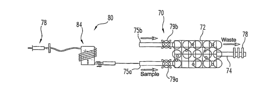
one embodiment of the invention may be configured as shown in FIG. 11. The
sensor 70 includes a MSPR substrate 72 with a T-shaped micro-fluidics
structure 74 mounted thereon. The T-shaped structure 74 operates in the
manner described above to direct fluid from the channels 75a, 75b of the
structure to the common channel 76 over the MSPR sensors. A second level
26
CA 02634027 2008-06-12
WO 2007/075444 PCT/US2006/047959
of the micro-sensor 70 includes the fluid control components. In particular, a
micro-fluidic pump 78 is provided at the discharge end of the common channel
76. In specific embodiments, the pump may be peristaltic, thermal, or piezo-
actuated. Each channel 75a, 75b is provided with a corresponding micro-
valve 79a, 79b to control fluid flow through the respective channel into the
common channel 76. In a single analyte detection sensor, such as the micro-
sensor 70 shown in FIG. 11, one channel 75a and valve 79a controls flow of
the sample into the common channel, while the other channel 75b and valve
79b controls flow of the functionalization solution.
It is contemplated that the micro-fluidics components may be
electronically controlled to operate in a pre-determined sequence for
functionalizing the MSPR sensor array and analyzing a fluid sample. In
particular, valve 79a may be closed and valve 79b opened to permit
introduction through channel 75b of functionalization solutions, such as the
functionalization composition as described above. Once the SPR sensors are
functionalized, a buffering solution may be introduced through the channel
75b.
The valve 79b may then be closed and valve 79a opened to accept the sample
fluid through channel 75a to contact the fully functionalized SPR sensor
array.
Of course, it is contemplated that the functionalization step may occur remote
from the sample analysis - i.e., in the preparation of a pre-packaged
biological
micro-sensor.
In addition, the pump and micro-valves may be controlled as necessary
to ensure sufficient formation of the monolayer of the target on the
functionalized MSPR sensor. For instance, in the Gox example above, the
formation of a 160,000 Da monolayer about 10nm thic: was detected with a
time constant of about 562 seconds. Thus, the flow of test fluid through the
micro-fluidics chamber must be adequate to ensure the formation of a
significant and detectable monolayer of the target.
Another aspect of the fluidics element of the inventive sensors is
dependent upon the nature of the fluid sample being evaluated. In particular,
a
complex sample requires cleaning and pre-concentration before analysis to
ensure accurate detection results. Such complex samples include human
2 7
CA 02634027 2008-06-12
WO 2007/075444 PCT/US2006/047959
blood, which may be evaluated for certain proteins as described in the
functionalization examples above, and natural water, such as water from a
river
being evaluated for the presence of dangerous pathogens. Pre-cleaning and
pre-concentrating a biological sample may occur prior to introduction into the
MSPR sensor system. For instance, centrifugation may be used to clean a
fluid sample, but centrifuge machines are not adapted for a micro-fEuidics
environment. Large-scale sample testing, such as a drinking water purity
monitor, may be amenable to this scale of pre-cleaning and pre-concentrating.
However, one feature of the present invention is that is very well suited for
micro-fluidics applications in which the entire sensor and associated sample
fluidics are present on a single small chip.
Thus, the present invention contemplates the addition of micro-fluidic
filtration and pre-concentration modules that are integrated onto the MSPR
sensor chip. Thus, a system 80 shown in FIG. 12 may incorporate a micro-
fluidic filter module 82 and a pre-concentration module 84 upstream of the
MSPR sensor chip, such as the chip 70 illustrated in FIG. 11. In this
embodiment, the upstream modules are connected to -Lne fluid sample channel
75a and valve 79a.
The micro-fluidic filter 82 in a specific embodiment includes a porous
membrane sandwiched between opposing PDMS molds. The flow area of the
filter depends upon the fluid sample being tested. For instance, a filter area
of
about 2.5 cm2 is sufficient for low volume filtering, such as up to 1 ml of
blood.
Larger filter areas may be required for higher volume, or higher flow rate
sampling.
In general, filtration removes some of the targets that are desired to be
detected. For instance, many proteins will non-specifically bind to filter
membranes. Thus, in some cases a pre-concentration module 84 may be
interposed between the filter module 82 and the sample channel 75a of the
micro-fluidics sensor chip. A variety of pre-concentration approaches may be
acceptable, such as electrophoresis, capillary separation, functionalized
magnetic bead, isotachophoresis, column separation or photo-activated
polycarbonate (PPC) micro-fluidics chips.
28
CA 02634027 2008-06-12
WO 2007/075444 PCT/US2006/047959
The small size and the accuracy of the MSPR sensor chip of the present
invention allows the fabrication of sensors with throughput and massively
parallel processing capabilities that greatly exceed the capabilities of
current
sensors and biosensors. In particular, the MSPR sensors of the present
invention can be configured to detect thousands and even millions of targets,
all on a single small sensor chip. As shown in FIG. 13 the sensor chip
includes
a plurality of MSPR beads on a single chip that may be arranged in randomly
mono-dispersed arrays or in regular arrays. The arrays of MSPR sensors may
be produced using photolithography and/or holographic optical tweezing, or any
other suitable technique for placing microscopically small objects onto a
glass
substrate. However, one feature of the present invention is that millions of
the
micro-sized MSPR beads may be completely randomly dispersed on the
substrate using currently available technology. As explained below, in spite
of
this random dispersion of MSPR beads, sensors made according to this
embodiment of the invention may be fully functionalized to detect a vast
number of targets.
In order to accommodate the need to detect multiple target, current
planar SPR sensor technology requires uniformly distributed SPR elements to
ensure adequate detection capabilities for multiple targets. The relatively
low
sensitivity of these current sensors dictates that a sufficient number of SPR
elements be associated with predetermined "spots" in which all elements are
functionalized to a particular target. However, the ability to accurately
place
uniformly distributed SPR elements is very limited, generally not exceeding a
100 by 100 grid of elements. This limitation, coupled with the accuracy
limitations of the current planar sensors, uitimately limits the number of
discrete
targets that can be detected to less than about 1000, which ultimately
severely
limits the range of applications for these sensors. For i.nstance, gene
therapy
and human genome mapping projects yield millions of targets for detection.
Using the current planar technology, hundreds of the bulky sensors would be
necessary for projects of this nature.
On the other hand, the capability exists to randomly disperse the micro-
beads utilized in the sensor of the present invention. However, until the
?9
CA 02634027 2008-06-12
WO 2007/075444 PCT/US2006/047959
present invention, there has been no way to capitalize on this ability to
populate
a sensor substrate with millions of SPR elements, each capable of being
functionalized individually or in groups of spots. In accordance with the
present
invention, one method of achieving this discrete functionalization is to
operate
on groups of sensors by flowing reagents over specific bands of the sensor
chip using micro-fluidics. In other words, as seen in FIG. 13 the chip 72 may
be divided into multiple bands, such as the four lengthwise bands 86a-d. A
micro-fluidics system may then flow a specific reagent along each band to
commonly functionalize each MSPR sensor along the band. This approach
limits the degree of functionalization to the number of bands on the chip over
which the various reagents may accurately flow. In one specific embodiment,
the MSPR chip may be divided into about twenty bands, each with different
functionalization so that a like number of targets may be earmarked for
detection.
-In another approach, individual MSPR sensors may be precisely
selected for specific functionalization. One manner of achieving this
individual
functionalization may be by use of a photo-activation bound cross-linker, such
as photo-biotin. However, this method is inherently slow since only a few SPR
sensors maybe functionalized at a time. Another more versatile approach is to
use a micro-spotter for making micro-arrays of SPR bead sensors, in a manner
similar to prior ink jet printers. Some micro-spotter printers are capable of
placing ink drops to a resolution of 600x600 dpi, with dot sizes in the range
of
30pm at 45pm spacing and a volume of only 10 p!. Even more accurate ink jet
printers are capable of resolutions of 4800x4800 dpi with each ink dot having
a
diameter of only 5pm. This printing technique may be adapted to functionalize
selected MSPR sensors or groups of sensors, resulting in functionalized spots,
such as the spots 88 shown in FIG. 13. Each spot may pertain to a different
target.
In yet another approach, discrete multiple target functionalization may be
achieved using a multi-pin spotter. This multi-pin spotter may precisely apply
the cross-linker or reagent directly to and only on the MSPR beads. The
CA 02634027 2008-06-12
WO 2007/075444 PCT/US2006/047959
specifically functionalized beads may be in clusters or randomly dispersed
throughout the entire field of MSPR beads.
In a further approach to functionalization that is well suited to massively
parallel processing, the MSPR beads may be functionalized using a mask. The
mask limits the application of the cross-linker or reagent to the MSPR beads
disposed within spots 88 on the substrate. It is contemplated that the
functionalized spots will encompass random numbers of the randomly
dispersed MSPR beads on the array over an area that is significantly larger
than the beads themselves. Thus, in a specific embodiment, the functionalized
spots may occupy an area about 30pm in diameter, whereas the MSPR beads
have a diameter of about 770 nm. A micro-spotter capable of dispensing
reagents in quantities as low as 10 pl may be used to functionalize the beads
in
each spot. The sensor chip may include a bar code 86 or some other readable
signature identifying the various functionalizations as well as spots
corresponding to each functionalization. As described below, the bar code 86
may also contain calibration information corresponding to the responsive
signals generated by the detector 90 (FIG. 14).
With the sensor construction as thus far described, a plurality of
randomly dispersed MSPR beads populate the substrate, with collections of
beads commonly functionalized to form spots 88. In the specific example
shown in FIG. 13, eighteen such spots are depicted; however, it is
contemplated that hundreds, thousands and even millions of such spots may
be defined on a given sensor chip. An operational sensor chip requires a light
source and some form of detector to sense the resonant response at each
spot. Thus, in accordance with one embodiment of the invention, a stack
forming the micro-sensor may appear as shown in FIG. 14 with the MSPR
sensor chip 72 sandwiched between a detector 90, which may be a CCD array,
and a light source 96, which may be an LED. It is understood that various
optical conditioning elements may be integrated with the light source and/or
detector, such as an optical filter to improve signal/noise ratio. The optical
conditioning element may also include a wavelength filter or different
discrete
wavelength filters corresponding to specific spots 88 or individual MSPR
beads.
3I
CA 02634027 2008-06-12
WO 2007/075444 PCT/US2006/047959
In accordance with one feature, the detector or CCD array may be
mapped into a grid 92, with each pixel 93 of grid containing a CCD capable of
sensing light transmission through the MSPR sensor chip 72 and configured to
generate a signal indicative of that light transmission for subsequent
processing. This mapped grid 92 overlays the sensor chip, as shown in FIG.
14, or alternatively the spots 88 may be regarded as projected onto the
mapped grid, as illustrated in FIG. 13. Optimally, the detector grid is fine
enough so that each spot 88 may be projected onto multiple pixels 93 of the
grid. It is expected that each pixel may overlay several MSPR beads, although
the number of beads corresponding to each pixel will vary due to the random
distribution of the beads on the substrate.
Calibration of the detector proceeds first by identifying an optimum pixel
or pixels reading transmission data from each spot 88. Thus, in a specific
example, a particular spot may fully encompass four pixels 93 and partially
encompass five additional pixels. The MSPR chip is illuminated by the light
source 96 and the measured intensity at each of the pixels corresponding to
the spot is evaluated. The pixel registering the greatest response is selected
as the pixel corresponding to the specific spot, which in turn corresponds to
a
specific functionalization. That selected pixel will likely map onto the
largest
number of MSPR beads relative to the other pixels, hence its greater response
relative to the other pixels. The output from the CCD within this selected
pixel
may then be calibrated in relation to the intensity and/or wavelength of the
light
source 96. This same process is repeated for all of the other functionalized
spots 88. Thus, in the specific example, for the eightepn functionalized spots
(FIG. 13), eighteen pixels 93 on the mapped grid 92 of the detector 90 may be
identified so that the calibrated output of each pixel will be evaluated. This
calibrated output may be written onto an on-board memory or transmitted to a
peripheral memory device and/or processor. A calibration table with the
calibration data for each of the mapped pixels may be maintained in a memory
and accessed by the peripheral processor. The bar code 86 may thus provide
an identifier for extracting the proper calibration table from multiple tables
stored in memory. The calibration table may identify which pixels to read from
the detector and how to interpret the output signal from each pixel. The
32
CA 02634027 2008-06-12
WO 2007/075444 PCT/US2006/047959
peripheral device applying the calibration data may be configured to obtain
the
necessary data from a global database, such as through an Internet link.
It is contemplated that additional pixels may also be associated with a
particular spot, with appropriate modifications to the calibration of the *
corresponding output responses. It should be appreciated that in some cases
the output response for a given pixel may result from light transmission
through
only one MSPR bead present within a given spot and aligned with a given pixel,
while for another pixel the light transmission may be measured through several
MSPR beads. The random distribution of beads means that the number of
MSPR beads used to generate an output signal corresponding to each
functionalized spot is also random. However, the calibration step described
above can ensure that the targets can be quickly and accurately detected. The
high sensitivity of each MSPR bead in the MSPR sensor of the present
invention means that even a single MSPR bead may be sufficient for a
particular functionalized spot and detector array pixel.
It can be appreciated that the device illustrated in FIG. 14 may open
realms of target detection unavailable with prior sensor devices. As explained
above, a single MSPR sensor chip may be functionalized to thousands of
targets in a small package. The small size of the sensors of the present
invention allows the formation of massively parallel arrays of sensors for
DNA,
RNA and protein detection. The use of micro-fluidics with the sensor chip
allows for a continuous flow of test fluid across the sensor chip 70. This
micro-
fluidics feature facilitates the massively parallel sensor arrays and provides
an
avenue for real-time accurate sensing of chemical and biochemical conditions.
A particularly beneficial usage is in real-time detection of targets in the
blood stream. One important application of the multi-channel embodiments of
the present invention is in the detection of sepsis. Sepsis is a major source
of
mortality in post-surgery recovery and in trauma victims. Treatment of sepsis
is
largely limited to antibiotics and palliative measures to support heart, lung
and
kidney function. According to data collected in 2001, sepsis syndrome affects
an estimated 751,000 patients in the United States each year, of whom
383,000 (51.1 %) received intensive care. Mortality has been estimated at
CA 02634027 2008-06-12
WO 2007/075444 PCT/US2006/047959
215,000 deaths nationwide, increasing with age from 10% in children to 38.4%
in those 85 years and older. The cost per case averages about $22,000, which
means almost $17 billion annually. Early detection of sepsis and rapid
intervention (within two to four hours of onset) greatly reduces mortality and
debilitation in survivors. However, no current method exists to monitor
patients
for the onset of sepsis. In many cases the medication produced for sepsis
treatment failed due to the lack of instrumentation capable to continuously
monitor cytokines levels in patients' blood.
Sepsis syndrome is the body's systemic inflammatory response to
infectious stimuli. Endotoxins - such as lipopolysaccharide (LPS) from Gram-
negative bacteria, peptidoglycans and flagellan from Gram-negative and Gram-
positive bacteria, lipotechoic acid from Gram-positive bacteria, mannan from
fungi, and other antigens from infectious agents - stimulate macrophages and
monocytes to release tumor necrosis factor alpha (TNF-a), foilowed by a
cascade of cytokine release. During the first period of sepsis (especially the
first eight hours), excessive inflammatory response can cause massive organ
damage, especially to kidneys and heart, but also reaching the liver, lungs
and
brain, requiring artificial support of blood pressure and ventilation. This
organ
damage often causes debility or mortality months or years after the acute
phase of sepsis.
The release of pro-inflammatory mediators was originally thought to be
largely uncontrolled. However, subsequent investigations have demonstrated
that TNF-a also stimulates leukocytes to release anti-inflammatory cytokines,
including IL-10, IL-1 and transforming growth factor-beta (TGF- P), which
inhibit
the synthesis of pro-inflammatory cytokines and exert direct anti-inflammatory
effects on monocytes, macrophages, and endothelial cells. This compensatory
anti-inflammatory response syndrome (CARS) is intended to localize what
would otherwise be an uncontrolled pro-inflammatory response to the infection
throughout the body. Unfortunately, the anti-inflammatory response often
surpasses the pro-inflammatory response in the later phases of sepsis,
resulting in immunoparalysis - i.e., the inability to mount an effective
immune
response to additional infectious insults.
34
CA 02634027 2008-06-12
WO 2007/075444 PCT/US2006/047959
Thus, a minimally-invasive device, which could be attached to all
postoperative and post-trauma patients which could monitor the onset and
progress of sepsis, allowing for much earlier and more directed intervention,
and ultimately reducing both mortality and debility in survivors. In
accordance
with a particular embodiment, a micro-fluidics device 100, shown in FIG. 15,
is
provided that can be used to simultaneously analyze a set of six chemicals
that
play an important role in sepsis. (However, the micro-fluidic structure can be
modified to accommodate the analysis of more or fewer chemicals at the same
time, or may be modified for different driven flows, flow velocities or
analysis
set-ups). One manner of diagnosis of the onset of sepsis and its progress
involves monitoring the chemicals, TNF-a, IL-1, IL-6, IL-10, IL-13 and TGF-P,
at
the same time and in real time. Thus, as shown in FIG. 15, the micro-fluidics
sensor 100 includes a set of six channels 102-107 (each 50 pm wide, 100 pm
apart and 11 mm long in a specific embodiment) that come together into a
micro-fluidic chamber 110 (2 mm long and 600 pm wide), with each channel
corresponding to a particular monitored chemical. The spacing is chosen so
that diffusion of molecules of about 20kDa will not interfere with molecules
in
the neighboring channels. These six channels are used to functionalize the
sensor array 120 with specific anti-bodies for the above-mentioned chemicals.
The flow of different antibodies through the micro-fluidic chamber will create
a
series of six parallel antibody stripes 112, functionalizing the chip. The
chip
100 in this specific embodiment is designed for a flow of the antibody at a
minimum 400pm/s. This treatment and specific calibration can be done prior to
usage of this chip to evaluate a sample.
A transverse channel 116 of 200pm wide intersects the micro-fluidic
chamber 110. This channel is wider to permit more viscous and faster
coagulating fluids, like blood plasma, to pass though. The region of
intersection covers an area of 200pm x 600pm. The transverse channel 116
includes an inlet 117 through which the blood is introduced, and a waste
outlet
118. Similarly, the micro-fluidic chamber 110 includes a waste outlet 111.
This sensor array 120 is preferably oriented at the intersection of the
chamber 110 with the transverse channel 116 and preferably aligned with the
CA 02634027 2008-06-12
WO 2007/075444 PCT/US2006/047959
channel. In one specific embodiment, the sensor 120 may include a linear
array of six SPR bead sensors 124 or sensor spots, with each individual sensor
or sensor spot corresponding to a particular functionalization and aligned
with
the corresponding antibody strip 112.
The micro-fluidic device 100 depicted in FIG. 14 may be fabricated using
a poly-dimethylsiloxane (PDMS) substrate and a cover glass in the manner set
forth below. The devices are fabricated using negative-tone photoresist SU-8
as a master to cast PDMS channel structures. The master substrates are 50
mm x 50 mm glass slides. The substrates are cleeaned in HCI:HNO3 (3:1),
rinsed with nanopure water, dried with nitrogen, sonicated in methanol and
acetone (1:1), and dried with nitrogen again. The master is created with two
SU-8 photoresist layers. A first under-layer (an 18-20pm thick layer of SU-8
2010) is used to promote adhesion of the channel structure to the substrate
and a second thicker layer (60-80pm thick layer of SU-8 2070) of photoresist
is
used to create the channel structure. Both layers are processed identically
except that the first layer is exposed without a photomask. The photoresist is
spin coated on the substrate at 1000 rpm for 30 seconds and ramped at 40
rpm/second. After prebaking on a hot plate for one minute at 65 C and two
minutes at 95 C, the photoresist is then exposed to UV light. The proposed
channel design is transferred to the photoresist through a photomask drawn
using AutoCAD 2004 LT and printed on a transparency using a high resolution
laser printer at 8000 dpi. The UV exposure system is equipped with a high-
pressure Hg arc lamp filtered to pass 360 23 nm, and the exposure dose is
300mJ/cm2. The exposed photoresist is postbaked on the same hot plate for
one minute at 65 C and three minutes at 95 C. The master is then developed
for five minutes, rinsed with 2-propanol, and dried with nitrogen.
The silicone elastomer kit contains a polymer base and curing agent that
are mixed in a 10:1 ratio for five minutes. A tape barrier is placed around
the
mold to hold the elastomer mixture, and the elastomer is poured onto the
master. The PDMS on the mold is placed under low vacuum (-1 torr) for one
hour to enhance channel replication and cured by heat:ng at 120 C for twenty
minutes. The PDMS substrate is then separated from the master, and access
36
CA 02634027 2008-06-12
WO 2007/075444 PCT/US2006/047959
holes for fluid connections to the channels are punched through the elastomer
with a 16 G needle.
At the bottom of the PDMS mold, across the micro-fluidic chamber 110
at the intersection with transversal channel 116, the linear array of MSPR
beads 120 may be produced using photolithography and/or holographic optical
tweezing, or any other suitable technique for placing microscopically small
objects onto a glass substrate like using a micromanipulator and a laser
tweezers system. The micromanipulator is loaded with a solution of 103 - 102
beads/pL, precision-size-standard beads. This concentration is chosen so that
the MSPR beads of the array 120 are dispensed having a spacing of about 50-
100pm. An optical laser tweezers can be used to hold the bead in place until
the liquid dries and the next bead will be dispensed with the micromanipulator
and held with the tweezers until the liquid dries and so on and so forth. Once
the beads 124 are placed, the PDMS substrate is sputter coated through a
window of 1 mm x 1 mm placed above the intersection. The beads are covered
with 150nm of gold. The PDMS substrate and glass cover glass are then
permanently joined after being exposed to air plasma for 40 seconds prior to
contacting.
In one embodiment, a sepsis detector device may include a
catheterization tube connected intravenously to the patient and to a pumping
system to periodically draw a small volume of blood into the sensor device
100.
The blood passes through a disposable filter to extract the plasma and the
plasma is supplied to the disposable sensor 100 through a channel 116. The
output from the sensor provides a reading of the cytokine concentrations in
the
plasma. The waste blood passes through channel 118 to be collected in a
disposable biohazard-labeled discard tube. The small size of the MSPR sensor
and sensor chip of the present invention allows the sensor device 100 and
catheterization tube to be in place as long as the patient is under medical
care.
Control of the peristaltic pump to draw blood into the sensor chip may be
electronically controlled to occur at pre-determined intervals or in response
to
some other medical condition sensor. The detector of the sensor may be
37
CA 02634027 2008-06-12
WO 2007/075444 PCT/US2006/047959
coupled to the same controller to generate an alarm if the particular agents
are
detected.
Elevated levels of IL-10, IL-13 and TGF-P indicate incipient sepsis, while
elevated levels of IL-10, IL-13 and TGF-(3 indicate immunoparalysis. If the
sensing time for each of the sensors is too large, a single channel may not be
able to detect the cytokine levels in real time. In that case an array of
channel
detectors may be fabricated on a single disposable chip and the blood supply
switched between channels at five minute intervals. A controllable microvalve
may be used to alternately supply blood and clean sterile medium to the
sensors to reset them for the next measurement.
Classes of agonist and antagonist drugs have been developed to control
the various cytokines involved in sepsis. However, none of these drugs are
widely used because physicians have no way to monitor their effects, which
vary greatly from patient to patient and over time. The result is that the
current
treatment of choice includes inflammatory suppressors and enhancers that are
given in either insufficient or excessive doses, both of which may be lethal
to
the patient. The MSPR sensors of the present invention would allow
physicians to supply a tailored cocktail of agonists and antagonists which
would
suppress immune response early in infection and enhance it in late infection,
while maintaining the cytokines at optimal levels at all times.
The same principles for detecting sepsis conditions may be applied to
the interactive detection of other medical conditions, as well as an interface
to
collateral therapeutic devices. With appropriate functionalization, a single
or
multiple-sensor device may be used to monitor patient status during extended
treatments. For instance, a MSPR sensor chip and micro-fluidics system in
accordance with the embodiments described herein may be incorporated into a
dialysis system, or other device that continuously draws blood or other fluids
from a patient for treatment. The MSPR sensor chip may be integrated into a
continuous blood monitoring system to detect targets in real-time that are
indicative of oncoming problems, such as heart attack, stroke, kidney failure
and the like.
38
CA 02634027 2008-06-12
WO 2007/075444 PCT/US2006/047959
A second embodiment of the multiple sensor array devices may be
provided that comprises of a set of syringe tubes containing cytokine
regulatory
drugs and controlled by the output of the cytokine detector prescribed above.
This device would ultimately supply a controlled dosage of multiple cytokine
regulators to the patent via an intravenous (IV) drip, continuously changing
the
supply of agonists and antagonists to keep the patient's cytokines at optimum
levels. In the above blood monitoring example, the real-time detection of
targets indicative of the onset of a heart attack, for instance, may be used
to
provide immediate real-time dosing in response to the onset of that condition.
This same interventional treatment may be employed to stave off sepsis
when detected as described above. In this instance, certain anti-sepsis
treatments rely upon the action of a particular protein to inhibit the
creation of
certain target molecules. However, the treatment itself may be immune-
suppressant, so the treatment must be carefully administered. Real-time
detection of target levels by the MSPR and micro-fluidic sensors of the
present
invention allow prompt and accurate administration of the anti-sepsis
treatment.
A similar approach may be implemented to reduce the toxicity of chemo-
therapy or HIV treatments, or for other treatments that create target blood-
borne markers indicative of the onset or presence of unwanted side effects
The disposable MSPR sensor devices described above are suitable for
many other applications. For instance, the present invention may be adapted
for public and private drinking water testing. The MSPR sensors may be
functionalized to detect various organic and inorganic contaminants, toxins,
cellular organisms and viruses. The sensors may be positioned within the
water supply to continuously monitor the water flow for the selected targets.
Since the devices of the present invention rely upon light detection devices,
such as the CCD array 90 described above, an electrical signal is generated
that may be evaluated and used to initiate a predetermined response, such as
a sensible alert.
Devices based on these sensors can be developed for detection of
biohazards, noxious chemicals, neurotoxins, explosives, or HIV or other
viruses
or bacteria in blood, plasma or other body fluids. The present invention
allows
39
CA 02634027 2008-06-12
WO 2007/075444 PCT/US2006/047959
the sensors to be small enough to be portable and easily disposable. !n the
illustrated embodiments, the sensor chip fits within a 50mm x 50mm area.
Specific apparatus can be adapted for airport or homeland security use or for
use in water treatment plants or factories. Depending on the use, automated
systems for connecting to the input reservoirs of the chip can be included and
additional chemicals can be analyzed at the same time and on the same chip.
The 'MSPR sensors and micro-fluidics of the present invention may also
be adapted to monitor chemical reactions or bioreactions. The micro-chips of
the present invention may be integrated into fluid flow lines or directly
within
chemical reactors or bioreactors to detect certain target products of the
reactions or to detect the chemical conditions within the reactors that may
impact the reaction. The MSPR sensors may be used to optimize the reaction
conditions or determine when the reaction is complete. This specific
embodiment may have beneficial application as part of process control for drug
or chemical fabrication, especially to control the purity of the resultant
product.
Micro-fluidics devices endowed with the sub-micron cavity surface-
plasmon biosensors of the present invention overcome several deficiencies in
prior sensing techniques and devices. Combining the properties of the micro-
fluidics devices with the sensitivity of the MSPR bead sensor extends the
boundaries of the lab-on-a-chip ideal by increasing detection abilities inside
the
micro-fluidics chip or confined spaces.
Current devices monitor molecular interactions and molecular kinetics
using planar SPR or the older ELIZA kits. In order to excite surface plasmons
on a planar metal surface certain restrictions must be obeyed. In particular,
the
source of light must be p-polarized and a precise critical angle of incidence
must be obtained in order to produce a maximum coupling between incoming
photons and surface polaritons. The sensor of the present invention combines
the sensitivity of surface plasmons with the resonant properties of a
spherical
sensor. Besides a boost in sensitivity, the invention relaxes constraints on
the
geometry and polarization of the light source. Moreover, the sensor has a
footprint of a square micron or less, which makes it well-suited for
miniaturization (having an active area of about one thousand times smaller
than
CA 02634027 2008-06-12
WO 2007/075444 PCT/US2006/047959
the present state-of-the-art SPR planar sensors) while increasing sensitivity
and improving the ability to integrate into micro-fluidic structures.
Furthermore,
the MSPR sensors of the present invention work in transmission compared with
the prior SPR sensors that work in reflection. D-u-e to this difference, a
sensing
micro-fluidics chip incorporating the MSPR sensor of this invention can be
placed very close between the light source and th-e sensing window of the
detector, resulting in a very compact, robust an-d inexpensive handheld
device.
Micro-fluidics devices are currently the M-ust so,phisticated technology for
dealin,g with small quantities of analyte (ranging from picoliters to
microliters),
and for very precise control of flows and gradieftts. They are appropriate for
multiple replica molding and new configurations of cha-nnels and set ups can
be
produced at very low cost, making them suitable for single-use devices. This
property makes them convenient in many areas of research, especially for
medical applications. They are suitable for m-a-ssively parallel processing of
chemicals, which can save a huge amount of time, especially in analyzing very
complex samples, for example, but not limited to, blood plasma, body fluids,
toxic waste, foods, etc. The only time constra,in't is the reaction time
between
the specific molecular species in the sample and t'he receptors bound to the
surface of the functionalized MSPR detector.
The MSPR sensor of the present invention takes advantage of th=ese
proprerties of micro-fluidics devices. It has b=etter sensitivity than prior
devices
due to the coupling of the surface-plasmon with the geom=etry of the sensor.
While current SPR sensors can only detect la-rg-e molecules, the SPR sensors
of the present invention can detect large and small mole-cules with good
sensitivity. The smallness of the sensors allows control, detection and
analysis
to be achieved on a single chip and to take advantage of the ability of micro-
fluidics devices to conduct multiple parallel analyses, wfiiich can shorten
the
analysis time. Moreover, these device-s can be disposab~l'e and can be
pro-duced cheaply.
In the illustrated embodiments, the microspheres are coated with gold. It
is contemplated that the spheres may be coated with other metals, such as
silver, copper, or gold alloys. However, current exp-erimentation suggests
th,at
41
CA 02634027 2008-06-12
WO 2007/075444 PCT/US2006/047959
spectral resonances in the transmitted light occur only for gold-coated
spheres
or beads, which is believed to be due to the surface plasmon coupling. The
film thickness of the gold coating may be adjusted depending upon the
application of the particular MSPR sensor. However, it has been found that
increasing film thickness causes blue-shifting of the observed resonances, at
least for the symmetric (low frequency) mode. Conversely, it has also been
found that the frequency for the high frequency anti-symmetric mode is red-
shifted with increases in film thickness. Moreover, the spherical geometry
implemented in the present invention preferentially excites the symmetric SP
modes, thereby minimizing red-shift effects. Experimentation further suggests
that some peaks, such as the peak at 623 nm for a 770 nm bead coated with a
150 nm gold layer, exhibits much less sensitivity to the metal film thickness
than other peaks.
While the invention has been illustrated and described in detail in the
drawings and foregoing description, the same should be considered as
illustrative and not restrictive in character. It is understood that only the
preferred embodiments have been presented and that all changes,
modifications and further applications that come within the spirit of the
invention
are desired to be protected.
In the illustrated embodiments, the micro-particles forming the MSPR
sensor are spherical in shape to form a spherical resonant cavity. However,
other symmetric geometric shapes may be utilized for the bead shape. For
example, the bead may have an elliptical shape or be multi-faceted like a
dodecahedron, provided that the shape can sustain periodic boundary
conditions for the stationary plasmon wave to travel across the surface of the
bead.
The various materials and dimensions set forth for the illustrated
examples may also be modified while still maintaining the functionality
achieved
by the MSPR sensor and micro-fluidics systems of the present invention.
Modifications to the materials and dimensions of the MSPR sensor must still
fulfill the primary object of the MSPR sensors of the present invention,
namely
to detect targets Moreover, the modifications must not interfere with the
shape
42
CA 02634027 2008-06-12
WO 2007/075444 PCT/US2006/047959
or geometric resonant characteristics that are used to enhance the SPR
resonance features of the micro-cavity sensor. The detection capability of the
MSPR sensors of the invention relies upon binding the target to a coupling
reagent layer that it itself bound to the SPR-suppoi-ting coating, and
ultimately
upon the change in optical response.
It is believed that for most targets and coupling reagents the wavelength
of the applied light is not critical. On the other hand, the SPR-supporting
layer
is, by definition, wavelength dependent since the surface plasmon resonance
occurs in that layer. Thus, it is believed that modifications to the materials
and
dimensions of the MSPR sensor are centered on the selection of the SPR-
supporting layer material and its characteristic wavelength. In the
illustrated
embodiments, that material is gold which has a wavelength of 510nm. In
accordance with certain aspect of the invention, this wavelength determines
the
diameter of the micro-particles or beads 10 and the pinhole 16. The bead
diameter is also a function of the refractive index of the dielectric
material.
In alternative configurations, the SPR-supporting coating material may
be silver, copper, or other non-gold SPR-supporting material, with appropriate
changes in coating thickness. Since silver and copper each have a different
SPR characteristic wavelength, the selection of either metal as the material
for
coating 14 will result in a change in diameter for the micro-particle 10 and
the
pinhole 16. In accordance with certain embodiments of the invention, the
micro-particle diameter would be sized to about the characteristic wavelength
of the silver or copper coating, while the pinhole diameter would be fixed at
less
than that wavelength. Similarly, the coating thickness may be modified with a
commensurate change in the micro-particle and pinhole diameters.
To the extent that the MSPR sensor dictates the characteristic
wavelength, the light source and transmitted light detector (such as the
source
96 and detector 90 in FIG. 14) may be selected accordingly. In certain
embodiments, white light may be acceptable, while in other embodiments it
may be desirable to select a monochromatic light source centered at the
characteristic wavelength of the MSPR sensor. Preferably the light detector is
calibrated to the characteristic wavelength.
43
CA 02634027 2008-06-12
WO 2007/075444 PCT/US2006/047959
With respect to material selection for the MSPR sensors and micro-
fluidics chips of the present invention, the materials in the above examples
and
embodiments are illustrative. While the MSPR beads are described as formed
of polystyrene, other light transmissive materials may be used, such as glass
or
aluminum oxide. The selected material is most preferably dielectric and has an
index of refraction similar to polystyrene. Of course, as indicated above the
index of refraction of the bead material affects the optical response and
resonant mode of the MSPR, along with the SPR-supporting coating.
Likewise, the material forming the housing or chip around the MSPR
beads and substrate may be different from the PDMS material identified in the
illustrated examples and embodiments. Preferably, the material is
substantially
light transparent and exerts only a minimal influence on the optical and
resonance characteristics of the MSPR sensor.
With respect to applications or uses of the MSPR sensors and micro-
fluidic sensors of the present invention, the foregoing examples and
embodiments are not intended to be limiting. It should be appreciated that the
present invention permits the rapid and accurate detection of a wide range of
targets, whether in small sample volumes or in continuous flow systems. The
present invention also permits simultaneous detection of hundred, thousands
and even millions of targets in a single micro-sensor or in a massively
parallel
array of sensors. Thus, even as the present invention may greatly enhance
current detection techniques, it will likely lead to new techniques and
analyses
not yet contemplated.
44