Note: Descriptions are shown in the official language in which they were submitted.
CA 02634406 2008-06-19
WO 2007/087201 PCT/US2007/001165
Polarization light modulator
Technical field
[01] The invention relates generally to visual display devices and light
modulator systems. In particular it relates to differential, interferometric
light
modulator systems containing optical polarization-sensitive devices.
Background
[02] Display devices such as television sets and movie projectors often
incorporate a modulator for the purpose of distributing light into a two-
dimensional pattern or image. For example, the frames of a movie reel
modulate white light from a projector lamp into shapes and colors that form an
image on a movie screen. In modern displays light modulators are used to
turn on and off individual pixels in an image in response to electronic
signals
that control the modulator.
[03] Texas Instruments introduced a microelectromechanical light
modulator called a digital mirror device which includes millions of tiny
mirrors
on its surface. Each mirror corresponds to a pixel in an image and electronic
signals in the chip cause the mirrors to move and reflect light in different
directions to form bright or dark pixels. See, for example, U S Patent Number
4,710,732 incorporated herein by reference. Stanford University and Silicon
Light Machines developed a microelectromechanical chip called a grating light
modulator in which diffraction gratings can be turned on and off to diffract
light
into bright or dark pixels. See, for example, U S Patent Number 5,311,360
incorporated herein by reference.
[04] Both of these reflective and diffractive light modulation schemes for
displays involve two-dimensional arrays of light modulator elements.
However, it is also possible to make a display in which light is incident on a
linear array of high speed light modulators. With appropriate magnifying
optics and scanning mirrors, a linear array can be made to appear two-
Page 1 of 19
CA 02634406 2008-06-19
WO 2007/087201 PCT/US2007/001165
dimensional to an observer. Through the scanning action of a vibrating mirror
a single row of light modulators can be made to do the work of as many rows
of modulators as would be necessary to provide a real two-dimensional
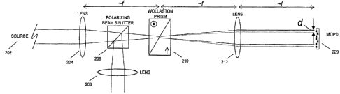
display of the same resolution. See, for example, U S Patent Number
5,982,553 incorporated herein by reference.
[05] Manhart introduced a display apparatus including a grating light-valve
array and interferometric optical system. See US Patent Number 6,088,102
incorporated herein by reference. In Manhart a display system employs a
planar grating light-valve (GLV) array as a spatial light modulator for
representing an image to be displayed. The system relies for image
representation on the position of moveable reflective elements of the GLV
array, which move through planes parallel to the plane of the array. The
moveable elements provide, from an incident phase-contrast wavefront, a
reflected phase-modulated wavefront representing the image to be displayed.
The displayed image is provided by interferometrically combining the phase-
modulated wavefront with a reference wave-front also formed, directly or
indirectly, from the incident phase-contrast wavefront.
[06] Many microelectromechanical light modulators are compatible with
digital imaging techniques. Digital information may be sent electronically to
the modulator. For example, gray scale images may be achieved by turning
pixels on only part time. A pixel that is switched from bright to dark with a
50% duty cycle will appear to an observer to have a constant intensity half
way between bright and dark. However, the pixel must be switched between
bright or dark states faster than the human eye's critical flicker frequency
of
roughly 30 Hz or else it will appear to flicker. Therefore two-dimensional
digital light modulators for displays must switch between states quickly to
display a range of light levels between bright and dark.
[07] A one-dimensional digital light modulator array, scanned by a vibrating
mirror to make it appear two-dimensional, must incorporate modulators with
fast switching speeds. Each modulator element must switch on and off
quickly to provide the impression of gray scale and this action must be
repeated for each pixel in a line within the scanning period of the mirror.
Grating light modulator devices in particular exhibit high switching speeds
Page 2 of 19
CA 02634406 2008-06-19
WO 2007/087201 PCT/US2007/001165
because their mechanical elements move only very short distances. The
grating light modulator incorporates parallel ribbon structures in which
alternating ribbons are deflected electrostatically to form diffraction
gratings.
The ribbons need only move a distance of one quarter wavelength of light to
switch a grating on or off. It is also possible (and desirable in many
instances)
to operate one- or two-dimensional light modulators in analog, rather than
digital, modes.
[08] Gudeman proposed an interferometric light modulator based on a
mechanical structure very similar to the grating light modulator; see U S
Patent Number 6,466,354 incorporated herein by reference. Gudeman's light
modulator is a form of Fabry-Perot interferometer based on a ribbon structure.
[09] Microelectromechanical light modulators typified by the Texas
Instruments' digital mirror device and Stanford / Silicon Light Machines
grating
light modulator devices mentioned above have already enjoyed wide
commercial success and have spawned other related designs. See, for
example, U S Patent Number 6,724,515 incorporated herein by reference.
[010] The digital mirror device is comparatively slow and therefore is usually
supplied as a two-dimensional mirror array. Usually two dimensional
modulator arrays are more expensive to make than one-dimensional arrays
and require a sophisticated addressing scheme for the mirrors. A two-
dimensional array requires defect-free manufacturing of N x N pixels over a
large chip area while a one-dimensional array with the same image resolution
requires only N working pixels on a chip in a single line.
[011] Grating light modulator devices, while very fast, have limitations due
to
diffraction. A grating light modulator has a reflective state or configuration
and
a diffractive state. In the diffractive state incoming light is diffracted
into the
+1 and -1 diffraction orders of an optical grating. However, only about 80% of
the light is collected in these two orders.
[012] An interferometric light modulator that has many desirable features was
disclosed in "Differential interferometric light modulator and image display
device," US 10/904,766 filed on November 26, 2004, incorporated herein by
reference. That device features high speed and high contrast. The
Page 3 of 19
CA 02634406 2008-06-19
WO 2007/087201 PCT/US2007/001165
interferometric design means that light is not lost in higher diffractive
orders
(as can be a problem in diffractive devices), nor does it require
discriminating
diffracted from undiffracted light.
[013] In US 10/904,766 a novel light modulator incorporates a polarizing
prism to split light beams into components of orthogonal polarization. These
polarization components are made to travel unequal distances in the
modulator and are then recombined in the prism. When one polarization
component is phase shifted with respect to the other, the overall polarization
of the recombined beam is transformed. The polarization of the recombined
beam is then analyzed by a polarizing beam splitter. Light intensity output
from the polarizing beam splitter depends on the polarization state of the
incident light beam which in, turn depends on the relative phase shift of the
polarization components.
[014] A phase shift is imparted to the orthogonal polarization components in
the modulator by focusing them on, and causing them to reflect from, an
engineered, uneven surface. This phase shift surface has regions of slightly
different displacement which cause the light beams to travel slightly
different
distances upon reflection. A novel microelectromechanical system (MEMS)
ribbon array device is provided that is used to modulate the phase shift of
light
beams reflected from the surface of its ribbons.
[015] Generalized and improved interferometric light modulators were
disclosed in "Differential interferometric light modulator and image display
system," US 11/161,452 filed on August 3, 2005, incorporated herein by
reference. Optical polarization displacement devices, designs for MEMS
optical phase shift devices and compensation schemes to improve field of
view were described.
[016] In US 11/161,452 a differential interferometric light modulator and
image display system comprises a polarizing beam splitter, a polarization
displacement device and a MEMS optical phase shifting device. A linear
array of MEMS optical phase shifting devices serves to modulate a line of
pixels in the display. The polarizing beam spiitter acts as both the polarizer
and the analyzer in an interferometer. The polarization displacement device
Page 4 of 19
CA 02634406 2008-06-19
WO 2007/087201 PCT/US2007/001165
divides polarized light from a polarizer into orthogonal polarization
components which propagate parallel to one another. The MEMS optical
phase shifting device, or array of such devices, imparts a relative phase
shift
onto the polarization components and returns them to the polarization
displacement device where they are recombined and sent to the analyzer.
The MEMS optical phase shifting devices are electronically controlled and
convert electronic image data (light modulation instructions) into actual
light
modulation.
[017] Further development is always possible, however. It would be
desirable to have a polarization light modulator design that is as compact as
possible. Brightness and high contrast are important features of displays and
are in need of continual improvement. For some applications, such as head-
mounted displays, a viewer designed to be placed close to an observer's eye
is needed.
Brief description of the drawings
[018] The drawings are heuristic for clarity.
[019] Figs. 1A - 1 D show schematically various polarization separating
optical elements.
[020] Figs. 2A & 2B show a design for a polarization light modulator.
[021] Figs. 3A & 3B show a design for a compact polarization light
modulator.
[022] Figs. 4A & 4B show a design for a polarization light modulator for
close-up viewing.
[023] Figs. 5A - 5C show schematically a MEMS optical phase shifting
device.
[024] Figs. 6A & 6B show schematically cross-sections of the device
illustrated in Fig. 5A.
[025] Figs. 7A & 7B show schematically a MEMS optical phase shifting
device with an aperture.
Page 5 of 19
CA 02634406 2008-06-19
WO 2007/087201 PCT/US2007/001165
[026] Fig. 8 shows schematically a MEMS optical phase shifting device with
an aperture wider than that illustrated in Fig. 7A.
Detailed description
[027] Display systems manipulate light to form images of text, graphics and
other visual scenes. Light propagation involves a complex variety of
phenomena including wave properties and polarization. In related
applications, US 10/904,766 and US 11/161,452, a new class of display
systems was introduced that comprise polarization interferometers combined
with MEMS devices that shift the phase of optical waves.
[028] In these new systems a linear array of MEMS optical phase shifting
devices serves to modulate a line of pixels in a displayed image. A polarizing
beam splitter acts as both the polarizer and the analyzer in an interferometer
while a polarization displacement device divides polarized light from the
polarizer into orthogonal polarization components. The MEMS optical phase
shifting device array imparts a relative phase shift onto the polarization
components and returns them to the polarization displacement device where
they are recombined and sent to the analyzer. The MEMS optical phase
shifting devices are electronically controlled and convert electronic image
data
(light modulation instructions) into actual light modulation.
[029] In the interferometric light modulators disclosed in US 10/904,766 and
US 11/161,452, the direction of polarization displacement is parallel to the
ribbons or cantilevers in the MEMS optical phase shift device. This means
that the light forming a particular pixel comes from light that was reflected
from different parts of a single ribbon or cantilever.
[030] In this application a different optical arrangement is disclosed in
which
orthogonal polarizations are displaced perpendicular to ribbons in a MEMS
optical phase shift device. Accordingly, light forming a displayed pixel comes
from light reflected from more than one ribbon or cantilever. Also disclosed
herein are optical designs for compact polarization light modulators and
displays for close up viewing. Designs for MEMS optical phase shift devices
are presented including optimizations for high power handling.
Page 6 of 19
CA 02634406 2008-06-19
WO 2007/087201 PCT/US2007/001165
[031] A polarization light modulator display relies on interferometry to
modulate pixels in a displayed image. Interferometry in turn depends on
manipulating the phase of light to produce constructive or destructive
interference. An important part of a polarization light modulator is a device
that separates polarization components of light so that the relative phase
between them can be changed.
[032] Figs. 1A - 1 D show schematically various polarization separating
optical elements. Elements shown in Figs. 1A - 1 D were introduced in related
applications US 10/904,766 and US 11/161,452; however, additional features
are described here.
[033] In Figure IA a Wollaston prism is shown. Figure 1 B shows a
Wollaston prism in combination with a lens placed one focal distance away.
Figure 1 C shows a Savart plate. Figure 1 D shows a generalized polarization
displacement device.
[034] The Wollaston prism shown in Figure IA splits incoming light beam
102 into orthogonally polarized components 112 and 114. Light beams 112
and 114 propagate away from each other indefinitely since they exit the prism
at different angles. The Wollaston prism is composed of two pieces of
material 104 and 106 with optic axes oriented as shown by arrows 108 and
110.
[035] Dashed arrow 116 indicates that translation of the Wollaston prism
perpendicuiar to incoming, light beam 102 varies the properties of light beams
112 and 114. Translation varies the phase difference between the beams and
therefore can be used to adjust the set point of an interferometer.
Additionally, the prism can be tilted in the plane of the paper (i.e. about an
axis perpendicular to the plane of the paper). Tilt can be used to make small
adjustments in the separation angle, e. This degree of freedom is helpful
when matching polarization displacement to the distance from one ribbon to
an adjacent ribbon in a MEMS optical phase shift device.
[036] Figure 1 B shows a lens 160 placed one focal length away from a
Wollaston prism. This situation is similar to that shown in Figure 1A except
that the orthogonally polarized light beams 156 and 158 exiting the system
Page 7 of 19
CA 02634406 2008-06-19
WO 2007/087201 PCT/US2007/001165
are parallel to one another. It is desirable that polarization displacement
devices have this property, namely that light beams leave them parallel to one
another. That way the beams retrace their path upon reflection from a MEMS
optical phase shifting device. The separation, d, is related to the focal
length,
f, and the separation angle, 6, according to d = f- 9 when is a small angle.
[037] It is normally advantageous to replace two optical components with one
whenever possible. Such a replacement is accomplished by the Savart plate
illustrated in Figure 1 C. A Savart plate is an example of a walkoff crystal
which imparts lateral displacement on polarization components of light
incident upon it. (A Wollaston prism is an example of a birefringent prism
which imparts angular separation on polarization components.) In Figure 1C
input light beam 122 is divided into orthogonally polarized components 132
and 134. The Savart plate is composed of two pieces of material 124 and 126
with optic axes oriented as shown by arrows 128 and 130. Arrow 130 is
dashed to indicate that it does not lie in the plane of the page; in fact, it
forms
a 45 degree angle with the plane of the page.
[038] Distances LT and L2 indicate that thicknesses in the Savart plate vary
the properties of light beams 132 and 134. These thicknesses can be
designed to specify the set point of an interferometer. Additionally, the
plate
can be tilted in the plane of the paper (i.e. about an axis perpendicular to
the
plane of the paper). Tilt can be used to make small adjustments in the
separation distance, d. This degree of freedom is helpful when matching
polarization displacement to the distance from one ribbon to an adjacent
ribbon in a MEMS optical phase shift device.
[039J In general any device can be used as a polarization displacement
device as long as it has the effect shown in Figure 1 D. An incoming light
beam 162 is separated into two parallel light beams 164 and 166 which are
polarized orthogonal to one another. Equivalently, if polarized light beams
164 and 166 are considered the input, then the device combines them into
one beam 162. The polarization of beam 162 is then determined by the
relative phase of the polarization components of beams 164 and 166.
Page 8 of 19
CA 02634406 2008-06-19
WO 2007/087201 PCT/US2007/001165
[040] As described here and in US 10/904,766 and US 11/161,452, a
polarization displacement device may be made from a Wollaston, Rochon or
Senarmont prism in combination with a lens, a Savart plate or a modification
thereof, or any other optical components which have the same effect.
[041] Figs. 2A & 2B show a design for a polarization light modulator. Figs.
2A and 2B are views of the same design from perpendicular perspectives.
For convenience Fig. 2A may be referred to as a "top" view while Fig. 2B may
be referred to as a "side" view.
[042] In both views, light from source 202 propagates through various optical
elements before reflecting from MEMS optical phase shift device (MOPD)
220. On the return trip from MOPD 220 toward source 202 part of the light is
deflected toward lens 208 by polarizing beam splitter 206. This is illustrated
in
Fig. 2B only; in Fig. 2A lens 208 is hidden behind polarizing beam splitter
206.
[043] Light from source 202 is focused at different places in different
planes.
For example in Fig. 2A the light is diverging from source 202 toward lens 204.
In fact the source is placed approximately one focal length away from the lens
so that light is collimated between lenses 204 and 212. MOPD 220 is placed
approximately one focal length away from lens 212 such that the lens focuses
light on it. Viewed from the perpendicular direction in Fig. 2B, however,
light
from source 202 is approximately collimated. Therefore, after the light passes
through lens 204, travels a distance approximately equal to the combined
focal lengths of lenses 204 and 212, and passes through lens 212, it is
approximately collimated when it reaches MOPD 220.
[044] An equivalent description is that light at MOPD 220 is focused in a
narrow, slit-shaped cross section. At MOPD 220 the light is elongated
perpendicular to the plane of the paper in Fig. 2A and in the plane of the
paper in Fig. 2B. As described below this elongated illumination of the ribbon
array in MOPD 220 is advantageous for efficient use of light and
corresponding high brightness in a display.
[045] Wollaston prism 210 and lens 212 form a polarization displacement
device as described in US 10/904,766 and US 11/161,452. Accordingly
. Page 9 of 19
CA 02634406 2008-06-19
WO 2007/087201 PCT/US2007/001165
different polarization displacement devices may be substituted for them
without altering the principle of operation of the polarization light
modulator.
[046] The spatial relationship between the elongated focusing direction and
the polarization displacement direction of the light in Figs. 2A and 2B
differs
from that of previous designs described in US 10/904,766 and US
11/161,452. In previous designs the polarization displacement device
separated light into slit-shaped beams that were offset in a direction
perpendicular to the long axis of the slit-shaped cross section. Here the
polarization displacement device (i.e. Wollaston prism 210 and lens 212)
separates light into slit-shaped beams that are offset in a direction parallel
to
the long axis of the slit-shaped cross section. This is indicated by dotted
lines
in Fig. 2B which show part of the light in the system displaced by a distance,
d, at MOPD 220. The displacement is not visible in Fig. 2A because it is
perpendicular to the plane of the paper.
[047] Polarization components of light arriving at MOPD 220 are offset
perpendicular to the ribbons in the MOPD. This is also illustrated in Fig. 7A,
for example, where region 734 (bounded by a heavy dashed line)
encompasses orthogonal polarizations of light that are offset by the width of
ribbon 506 or 508 in a direction perpendicular to the ribbons and in the plane
of the paper.
[048] In Figs. 2A and 2B it is helpful if source 202 is a line source;
however, if
it is not, its shape can be modified by beam shaping optics (not shown).
Polarizing beam splitter 206 acts as both the polarizer and the analyzer in
the
interferometer that it forms with the polarization displacement device
(Wollaston prism 210 and lens 212) and the MOPD 220. Two arms of the
interferometer are formed by orthogonal polarizations of light which travel
slightiy different paths to and from the MOPD.
[049] In Figs 2A and 2B source 202 is in line with lens 204, polarizing beam
splitter 206, Wollaston prism 210, lens 212 and MEMS device 220. Light
reflected by polarizing beam splitter 206 toward lens 208 forms a line image
which may be scanned to create a two dimensional image. It is entirely
possible however to place the light source in a position where lens 208 would
Page 10 of 19
CA 02634406 2008-06-19
WO 2007/087201 PCT/US2007/001165
focus its light into the optical system and to form a line image where source
202 is shown. The choice between these two equivalent arrangements
depends on practicalities such as contrast achieved by the polarizing beam
splitter in transmission versus reflection, and the shape of the light source
used.
[050] Figs. 3A & 3B show a design for a compact polarization light
modulator. Figs. 3A and 3B are views of the same design from perpendicular
perspectives. For convenience Fig. 3A may be referred to as a "top" view
while Fig. 3B may be referred to as a "side" view. In the figures source 302
provides light that converges to a waist near MOPD 320 when viewed from
the perspective of Fig. 3A but is collimated when viewed from the
perpendicular perspective of Fig. 3B. Examples of suitable sources include
line sources or point sources shaped by cylinder lenses (not shown).
[051] PDD 311 is a "polarization displacement device" as that term is defined
in US 11/161,452. Its function is to offset orthogonally polarized components
in an incoming light beam into two parallel beams of light. An example of a
polarization displacement device is a polarizing prism, such as a Wollaston or
Rochon prism, in combination with a lens. MOPD 320 is a "MEMS optical
phase shift device" as that term is defined in US 11/161,452. Its function is
to
impart an electronically controllable phase shift upon incident light. Many
types of MOPD were discussed in US 11/161,452. Details of one MOPD are
discussed here in connection with Figs. 5 - 8.
[052] In Fig. 3B lens 308 is placed approximately one focal length away from
MOPD 320. The lens is not shown in Fig. 3A because it is hidden behind
polarizing beam splitter 306 in that view. Also drawn in Fig. 3B is a graph
330
of light intensity, /, versus position, x, in the focal plane of lens 308. In
other
words the dotted x-axis of graph 330 and MOPD 320 are both approximately
one focal length away from lens 308, albeit in opposite directions. Two
intensity plots 332 and 336 are drawn on graph 330. Item 340 is a double-slit
aperture or stop.
[053] The dotted x-axis of graph 330 lies in the Fourier plane for MOPD 320.
Thus when MOPD is modulated, for example, in a square wave pattern where
Page 11 of 19
CA 02634406 2008-06-19
WO 2007/087201 PCT/US2007/001165
every other ribbon is deflected, the light intensity at the Fourier plane will
be
approximately that shown by plot 332. When the MOPD is unmodulated, i.e.
when no ribbons are deflected, the light intensity at the Fourier plane will
be
approximately that shown by plot 336.
[054] The available contrast between dark -and light states in the
polarization
light modulators described so far is determined mainly by the ability of the
polarizing beam splitter to discriminate between polarizations. In an ideal
case all light of one polarization is transmitted by the polarizing beam
splitter
while all light of the orthogonal polarization is reflected. In practice,
however,
some light in the "wrong" polarization leaks through or is reflected
unintentionally.
[055] Double-slit aperture or stop 340 may be used to increase contrast in a
polarization light moduiator. If aperture 340 is placed at the Fourier plane
of
lens 308 it blocks light when MOPD 320 is unmodulated but passes light
when the MOPD is modulated. This increases the contrast that is provided by
the polarization discrimination of polarizing beam splitter 306.
[056] The dotted x-axis of graph 330 lies in the Fourier plane of the MOPD
as a whole; however, it is not the image plane for pixels in the line image
that
are modulated at the MOPD. When lens 308 is placed one focal length from
MOPD 320, the line image is formed at infinity. The image can be brought
closer to the lens by moving the lens away from the MOPD in accordance with
the lens-maker's formula 1/dy + 1Id2 = 11f where di and d2 are distances to
the image and the MOPD measured from the lens. Alternatively the image
may be viewed with additional optics (not shown).
[057] Figs. 4A & 4B show a design for a polarization light modulator for
close-up viewing. Such a design is appropriate for head-mounted displays .
where the observer's eye is close to the device.
[058] Figs. 4A and 4B are views of the same design from perpendicular
perspectives. For convenience Fig. 4A may be referred to as a "top" view
while Fig. 4B may be referred to as a "side" view. In the figures, source 402
provides light that is collimated when viewed from the perspective of Fig. 4A,
but is diverging toward lens 404 when viewed from the perpendicular
Page 12 of 19
CA 02634406 2008-06-19
WO 2007/087201 PCT/US2007/001165
perspective of Fig. 4B. In Fig. 4B the source diverges from a location such
that lens 404 collimates the light; i.e. the source is approximately one focal
length away from lens 404. Examples of suitable sources include line sources
or point sources shaped by cylinder Ienses (not shown).
[059] Item 406 in the figures is athin polarizingbeam splitter that also acts
as a scanning mirror. It can be rotated about an axis (not shown)
perpendicular to the paper in Fig. 4B. The curved arrow near the thin
polarizing beam splitter 406 in Fig. 4B indicates the approximate scanning
motion. Lens 407 is located approximately one focal length away from MOPD
420; item 411 is a polarization displacement device.
[060] Viewed from the perspective of Fig. 4A light is focused to a waist
between lenses 404 and 407 while it remains collimated between those two
lenses in the perpendicular perspective of Fig. 4B. The focus need not
coincide with the position of thin polarizing beam splitter 406.
[061] The eye of an observer is drawn schematically in Fig. 4B as item 424;
the tens of the eye is item 426. When lens 407 is placed one focal length
from MOPD 420 the image of the MOPD appears at infinity. However, the
lens 426 in the eye 424 of an observer forms the image on the retina in the
back of the eye for easy viewing. The image is a line image that originates
from a thin sheet of light modulated by a linear array of electronically
controlled phase shifting surfaces in the MOPD. When thin polarizing beam
splitter 406 rotates, the line image moves across the retina in an observer's
eye. This scanning motion is used to create a two dimensional image from
the line image.
[062] Figs. 5A - 5C show schematically a MEMS optical phase shifting
device. Figs. 5B and 5C are cross sections of Fig. 5A along the lines
indicated. In Figs. 5A - 5C item 502 is a substrate or support base; 504 is an
end support; 510 is an intermediate support. Items 506 and 508 are ribbon
structures; 506 is a ribbon supported by intermediate supports while 508 is a
ribbon without intermediate supports. In Figs. 5A - 5C only eight ribbons are
shown while an actual device may contain hundreds or thousands of ribbons.
The figure is schematic only.
Page 13 of 19
CA 02634406 2008-06-19
WO 2007/087201 PCT/US2007/001165
[063] Fig. 5B shows that at the cross section marked "5B" in Fig. 5A there
are no supports between the substrate and the ribbons. Conversely Fig. 5C
shows that at the cross sections marked "5C" in Fig. 5A there are supports for
every other ribbon. In Fig. 5A cross sections "5C" are marked approximately
1/3 of the way from the ends of the ribbons and this is a preferred
arrangement; however, other designs are possible. It is only important that
every other ribbon is stiffened, by supports or other means, and that the
center portion where light is reflected by the ribbons is free of supports.
[064] Devices of the type shown in Figs. 5A - 5C may be constructed using
any standard MEMS fabrication processes such as those outlined in US
10/904,766. Although the drawings are not to scale one may appreciate the
size of a typical device by noting that the ribbons are normally between about
one and one hundred microns long; they flex toward the substrate by roughly
0.05 to 0.5 microns.
[065] Figs. 6A & 6B show schematically cross-sections of the device
illustrated in Fig. 5A at the sections marked "6A" and "6B" respectively. All
of
the numbered items in Figs. 6A and 6B correspond to the like-numbered
items in Figs. 5A - 5C. Voltage signal or source 610 was not illustrated in
Figs. 5.
[066] When a voltage is applied to a ribbon that is only supported at its
ends,
as exemplified by ribbon 508, the ribbon flexes toward the substrate. The
distance, D, that the ribbon is deflected is approximately one quarter
wavelength of light in normal operation of an MOPD in the polarization light
modulators of Figs. 2- 4. Conversely when a voltage is applied to a ribbon
that is supported by intermediate supports, as exemplified by ribbon 506, the
ribbon flexes far less than in the unsupported case. Ribbon 506 in Fig. 6B is
drawn as not flexing at all; in practice it may flex slightly. The deflection
is a
nonlinear function of the distance between supports, however, so it can be
significantly different for the supported and unsupported ribbons.
[067] An advantage of using supports to stiffen alternating ribbons is that
each ribbon can be the same thickness and made from the same material.
However alternate methods besides supports may be used if the end result
Page 14 of 19
CA 02634406 2008-06-19
WO 2007/087201 PCT/US2007/001165
remains the same: alternating ribbons are deflected different amounts under
the influence of an applied voltage.
[068] Figs. 7A & 7B show schematically a MEMS optical phase shifting
device with an aperture. Fig. 7A shows a view of an MOPD similar to the view
shown in Fig. 5A while Fig. 7B shows a view similar to that in Fig. 6A. In
Figs.
7 however, an aperture 722 has been placed over the ribbon structure.
[069] In Figs. 7 items 502 - 610 are the same as like-numbered items in
Figs. 5 and 6. Item 710 is a spacer. Items 720 and 722 form an aperture
structure from a clear sheet 720 with an opaque coating 722. In Fig. 7A
aperture structure 720 / 722 is shown in a cutaway view. The hatched area
and dotted line represented by 730 show the approximate extent of an
elongated light beam incident upon the MOPD. Rays 731 also represent the
light beam as viewed from a direction perpendicular to the direction of
propagation.
[070] Bounded region 732 represents the transverse extent of light that has
passed through aperture structure 720 / 722 and is incident on the ribbons of
the MOPD. Within bounded region 732, area 734, which is delineated by a
heavy dashed border, shows the portion of the MOPD from which reflected
light makes up a single pixel in the line image output from a polarization
light
modulator such as any of the modulators illustrated in Figs. 2- 4.
[071] Aperture structure 720 / 722 prevents stray light that would not
contribute to a line image from being reflected by the MOPD ribbons.
Preferably the aperture does not affect the polarization of light reflecting
from
it. In Figs. 7 the aperture is shown as a being formed by a patterned, opaque
coating on a clear substrate such as glass; however, an aperture formed in
another way but performing the same function is also acceptable. The
aperture is separated from the ribbons of the MOPD by spacer 710. To keep
the aperture in the near field, the spacer thickness should be less than -
w2/A,
where w is the size of the aperture and A is the wavelength of light.
[072] Area 734 represents the area of the ribbon device from which reflected
light forms a single pixel in a line image. Area 734 is shown as being
approximately square in the figure, but it may be rectangular in practice. The
Page 15 of 19
CA 02634406 2008-06-19
WO 2007/087201 PCT/US2007/001165
length of one side of the area is set by the width of the open slot in
aperture
720 / 722. The length of a perpendicular side of the area is equal to the
width
of two ribbons in the MOPD. Recall that the PDD in the polarization light
modulators of Figs. 2- 4 provides an offset for one polarization of light
incident upon an MOPD. The magnitude of the offset is shown by "d" in Figs.
1 B - 1 D, 2B, and by dotted lines in Figs. 3B and 4A.
[073] The polarization light modulator is designed so that the offset matches
the width of a ribbon in the MOPD. That way the interferometer in the
polarization light modulator compares the phase of light-reflected by adjacent
ribbons in the MOPD. As one of the ribbons in an adjacent pair moves while
the other remains stationary, the phase of light reflected by the ribbons
varies
by 4rrDIA where D is the displacement of the moving ribbon and A is the
wavelength of the light.
[074] Fig. 8 shows schematically a MEMS optical phase shifting device with
an aperture wider than that illustrated in Fig. 7A. !n Fig. 8 bounded region
832 is drawn approximately twice as wide as corresponding bounded region
732 in Fig. 7; area 834 is similarly represented as a rectangle instead of
square 734. The figure does not purport to illustrate the precise aspect
ratios
of these areas; but the possibility of using different aspect ratios is
important.
Light beam cross section 830 has a less elongated shape than corresponding
beam 730.
[075] All other things being equal the light incident upon the MOPD in Fig. 8
is spread over a wider area than that in Fig. 7A. Therefore if a material
limitation makes it necessary to restrict the intensity (power per unit area)
of
light failing on the MOPD then more power can be applied to the MOPD in
Fig. 8 compared to that of Fig. 7A. Fig. 8 represents a design with more
power handling capacity and therefore one that can lead to a brighter
displayed image than the one in Fig. 7A. An incoming light beam can be
expanded for operation with a wider aperture slot as in Fig. 8 through the use
of cylinder optics.
[076] Polarization light modulators described herein focus light in an
elongated beam cross section on a linear array MOPD. Orthogonal
Page 16 of 19
CA 02634406 2008-06-19
WO 2007/087201 PCT/US2007/001165
polarizations are displaced parallel to the long axis of the elongated beam
cross section. Compact modulator designs optimized for high brightness and
contrast were described.
[077] As one skilled in the art will readily appreciate from the disclosure of
the embodiments herein, processes, machines, manufacture, means,
methods, or steps, presently existing or later to be developed that perform
substantially the same function or achieve substantially the same result as
the
corresponding embodiments described herein may be utilized according to
the present invention. Accordingly, the appended claims are intended to
include within their scope such processes, machines, manufacture, means,
methods, or steps.
[078] The above description of illustrated embodiments of the systems and
methods is not intended to be exhaustive or to limit the systems and methods
to the precise form disclosed. While specific embodiments of, and examples
for, the systems and methods are described herein for illustrative purposes,
various equivalent modifications are possible within the scope of the systems
and methods, as those skilled in the relevant art will recognize. The
teachings
of the systems and methods provided herein can be applied to other systems
and methods, not only for the systems and methods described above.
[079] In general, in the following claims, the terms used should not be
construed to limit the systems and methods to the specific embodiments
disclosed in the specification and the claims, but should be construed to
include all systems that operate under the claims. Accordingly, the systems
and methods are not limited by the disclosure, but instead the scope of the
systems and methods are to be determined entirely by the claims.
Page 17 of 19