Note: Descriptions are shown in the official language in which they were submitted.
CA 02635303 2008-06-26
WO 2007/073600 PCT/CA2006/002132
ENGINEERED STRUCTURE FOR SOLID-STATE LIGHT EMITTERS
CROSS-REFERENCE TO RELATED APPLICATIONS
[01] The present invention claims priority from United States Patent
Application No.
60/754,185 filed December 28, 2005, and 60/786,730 filed March 29, 2006, which
is
incorporated herein by reference.
TECHNICAL FIELD
[02] The invention relates to solid-state lighting devices, and in particular
to engineered
structures of semiconductor films including luminescent centers for use in
solid-state light
emitters.
BACKGROUND OF THE INVENTION
[03] The next generation of solid-state lighting is seeking to provide
advances in
brightness, efficiency, color, purity, packaging, scalability, reliability and
reduced costs. The
creation of light emitting devices from silicon based materials, upon which
the modem electronic
industry is built, has been the subject of intensive research and development
around the world.
The main obstacle has been the indirect energy gap of bulk silicon, which
limits the efficiency to
an extremely low level. However, one particular technology, based on silicon
nano-particles,
e.g. nanocrystals, formed through various techniques, has been able to
overcome this difficulty.
[04] Prior art light emitting devices, such as those disclosed in United
States Patents Nos.
7,081,664, entitled: "Doped Semiconductor Powder and Preparation Thereof',
issued July 25,
2006 in the name of Hill; and 7,122,842, entitled Solid State White Light
Emitter and Display
Using Same, issued October 17,m 2006 to Hill; and United States Published
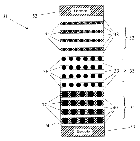
Patent Applications
Nos. 2004/151461, entitled: "Broadband Optical Pump Source for Optical
Amplifiers, Planar
Optical Amplifiers, Planar Optical Circuits and Planar Optical Lasers
Fabricated Using Group IV
Semiconductor Nanocrystals", published August 5, 2004 in the name of Hill;
2004/214,362,
entitled: "Doped Semiconductor Nanocrystal Layers and Preparation Thereof ',
published
October 28, 2004 in the name of Hill et al; and 2004/252,738, entitled: "Light
Emitting Diodes
and Planar Optical Lasers Using IV Semiconductor Nanocrystals", published
December 16, 2004
in the name of Hill, which are incorporated herein by reference, have
demonstrated that using
1
CA 02635303 2008-06-26
WO 2007/073600 PCT/CA2006/002132
[05] silicon-rich silicon oxide (SRSO), which consists of silicon nano-
particles embedded
in a silicon dioxide (Si02 or glass) matrix, reduces many of the problems
associated with bulk
silicon, and when doped with erbium, or other rare earth material, can exhibit
efficient room
temperature rare earth luminescence, because of the high efficiency of the
energy transfer
process from excited nanocrystals to rare earth ions. Accordingly, the SRSO
provides an
alternative to thin film electroluminescent material. The silicon nano-
particles act as classical
sensitizer atoms that absorb incident photons or electrons and then transfer
the energy to the rare
earth ions, which then fluoresce in the infrared or visible wavelength ranges
with several
advantages compared to the direct fluorescence of the rare earth. First, the
absorption cross-
section of the silicon nano-particles is larger than that of the rare earth
ions by more than three
orders of magnitude. Second, as excitation occurs via an Auger-type
interaction or via a F6rster
transfer process between carriers in the silicon nanoparticles and rare earth
ions, incident photons
need not be in resonance with one of the narrow absorption bands of the rare
earth.
Unfortunately, existing approaches to developing such silicon nano-particle
materials have only
been successful at producing very low concentrations of the rare earth
element, which is not
sufficient for many practical applications.
[06] Observations have shown that silicon nano-particles formed by such
techniques
generally have a relatively narrow distribution of photo-luminescent (PL)
wavelength or energy
despite the broad size distribution, i.e. the observed energies are not as
high as expected from the
quantum confinement of the nanocrystals. The reduced nano-particle excitation
energy affects
the efficiency of energy transfer from conducting electrons when these
structures are electrically
powered, thereby severely limiting the efficiency of light generation from
such films.
[07] In general, the manufacture of type IV semiconductor nano-particles doped
with a
rare earth element is done by ion implantation of silicon ions into a silicon
oxide layer, followed
by high temperature annealing to grow the silicon nano-particles and to reduce
the ion
implantation damage. The implantation of silicon ions is followed by an ion
implantation of the
rare earth ions into the annealed silicon nano-particle oxide layer. The
resulting layer is again
annealed to reduce the ion implant damage and to optically activate the rare
earth ion.
[08] There are several problems with this method:
2
CA 02635303 2008-06-26
WO 2007/073600 PCT/CA2006/002132
[09] i) it results in a decreased layer surface uniformity due to the ion
implantation;
[10] ii) it requires an expensive ion implantation step;
[11] iii) it fails to achieve a uniform distribution of group IV semiconductor
nano-
particles and rare earth ions unless many implantation steps are carried out;
[12] iv) it requires a balance between reducing the ion implant damage by
thermal
annealing while trying to maximize the optically active rare earth; and
[13] v) the thickness of the film is limited because implanted ions do not
penetrate deeply
into the film for practical implant energies.
[14] To diminish the above drawbacks, plasma enhanced chemical vapor
deposition
(PECVD) has been utilized to make group IV semiconductor nano-particle layers.
The prepared
layers are subjected to a rare earth ion implantation step, and a subsequent
annealing cycle to
form the group IV semiconductor nano-particles and to optically activate the
rare earth ions that
are doped in the nano-particle region. Unfortunately, the layers prepared with
this method are
still subjected to an implantation step, which results in poor surface
uniformity, non-uniform
distribution of rare earth elements, and limited film thickness.
[15] Another deposition method that has been used to obtain a doped group IV
semiconductor nano-particle layer consists of co-sputtering the group IV
semiconductor and rare
earth metal, typically in an oxygen plasma. In this method, the group IV
semiconductor and the
rare earth metal were placed on a target substrate, which was then placed into
a vacuum chamber
and exposed to an argon ion beam. The argon ion beam sputtered off the group
IV
semiconductor and the rare earth metal, both of which were deposited onto a
receiving silicon
wafer. The newly formed film on the silicon wafer was then annealed to grow
the nano-particles
and to optically activate the rare earth ions. The doped group IV
semiconductor nano-particle
layers made through this method have the drawbacks that: i) the layer does not
have a very
uniform distribution of nano-particles and rare earth ions; ii) the layer
suffers from up conversion
efficiency losses due to rare earth clustering in the film; and iii) the
concentration of rare earth
film in the film is limited to little more than 0.1%.
3
CA 02635303 2008-06-26
WO 2007/073600 PCT/CA2006/002132
[16] The concentration of the one or more rare earth elements in the
semiconductor nano-
particle layers is preferably as high as possible, as the level of response of
the film to external
stimuli, such as optical stimulation for photoluminescence, is proportional to
the concentration.
One problem encountered, when a high concentration of rare earth element is
present within the
semiconductor layer, is that when two rare earth metals come into close
proximity with one
another, a quenching relaxation interaction occurs that reduces the level of
optical response
observed. The concentration of the rare earth elements within a semiconductor
film is thus
balanced to be as high as possible to offer the most fluorescence, but low
enough to limit the
quenching interactions.
[17] Silicon nano-particles formed by such techniques generally have a
relatively wide
distribution of size, and a similarly wide spatial distribution, i.e. the
separation distance between
nano-particles, which affects the efficiency of energy transfer from
conducting electrons when
these structures are electrically powered. The average distance between nano-
particles in the
direction of electrical conduction must be large enough so that an electron
picks up enough
energy from the electric field between nano-particles to excite the light
emitting object and
produce a photon of the correct colour. However, because the spatial
distribution is isotropic, the
overall density of nano-particles in these films must be fairly low (-5x1O'$
cm Z). Unfortunately,
with such a low nano-particles density, and with a distribution of nano-
particle size and
separation, severe limitations are set on the efficiency of light generating
capability from such
films with embedded nano-particles.
[18] When rare earth ions are introduced in the film, it is desirable to
locate the rare earth
ions in the vicinity of the nano-particles to facilitate efficient energy
transfer from the excited
nano-particles to the rare earth ions. However, the ion implantation or in
situ deposition
techniques incorporate a random distribution of rare earth ions. In
particular, the generation of
white light requires multiple species of rare earths to be incorporated into
the films, since each
different species provides a different colour. It is impossible to ensure that
the correct rare earth
ion is located near the appropriate size of nano-particle so that the energy
of the excited nano-
particle is matched to the emissive wavelength of the rare earth ion. In other
words, it is highly
likely that the nearest rare earth ion radiates with too short a wavelength,
i.e. it cannot be excited
by the nano-particle, or too long a wavelength, i.e. energy is wasted in the
excitation process.
4
CA 02635303 2008-06-26
WO 2007/073600 PCT/CA2006/002132
Even if a high enough concentration of rare earths is used to avoid (at least
partially) such
mismatches of excited nano-particle energy to the radiative emission
wavelength of the rare earth
ion, losses still arise from interactions between rare earth ions when they
are closely spaced.
[19] In the films in which the nano-particles are formed with significant
variations in size
and separation distance, excess silicon atoms and dopants, such as rare earth
ions, are
incorporated uniformly throughout the films, but non-uniformly from a local
viewpoint.
Therefore, there is a chance that some of the excess silicon atoms may be
located far from any
nucleation site and may not precipitate into the nano-particles, but instead
will remain distributed
in the silicon dioxide host matrix. In addition, some rare earth ions may also
not be located close
enough to the nano-particles. Finally, if significant carbon content must be
incorporated into the
nano-particles to raise their excitation energy, the carbon atoms need to be
located close to the
nano-particles. It has been observed in general that without carbon
incorporation, silicon
nanocrystals with 2 nm diameter should have exciton energy of the order of 2.3
eV from the
quantum confinement effect, but it is observed that they only radiate in the
range of 1.4-1.8 eV.
If impurities, such as excess silicon atoms, rare earth ions, and carbon
atoms, remain in the oxide
matrix, they could severely impact the physical properties of the oxide,
particularly the
breakdown field and hence device reliability and lifetime.
[20] An object of the present invention is to overcome the shortcomings of the
prior art by
providing a multi-layered engineered structure in which wide bandgap
semiconductor or
dielectric buffer layers are disposed adjacent very thin active luminescent
layers designed to emit
light at a specific wavelength. The buffer layers provide the exact distance
in the direction of
electrical conduction so that an electron picks up enough energy from the
electric field when
passing through the buffer layers to excite luminescent centers in the active
layers to produce a
photon of the correct color via impact ionization or impact excitation.
SUMMARY OF THE INVENTION
[21] Accordingly, the present invention relates to a light emitting structure
comprising:
[22] a first active layer including a concentration of luminescent centers for
emitting light
at a first wavelength;
CA 02635303 2008-06-26
WO 2007/073600 PCT/CA2006/002132
[23] a first buffer layer comprising a wide bandgap or dielectric material
adjacent the first
active layer; and
[24] a set of electrodes for applying an electric field to the first active
and first dielectric
layers;
[25] wherein the first buffer layer has a thickness whereby electrons gains
sufficient
energy from the electric field when passing through the first buffer layer to
excite the
luminescent centers in the first active layer via impact ionization or impact
excitation at a
sufficient excitation energy to emit light at the first wavelength.
BRIEF DESCRIPTION OF THE DRAWINGS
[26] The invention will be described in greater detail with reference to the
accompanying
drawings which represent preferred embodiments thereof, wherein:
[27] Figure 1 is a cross-sectional view of an electroluminescent solid-state
device in
accordance with an embodiment of the present invention;
[28] Figure 2 is a cross-sectional view of a super-lattice semiconductor
structure in
accordance with the device of Fig. 1;
[29] Figure 3 is a cross-sectional view of an alternative super-lattice
semiconductor
structure in accordance with the device of Fig. 1; and
[30] Figure 4 is a cross-sectional view of an alternative super-lattice
semiconductor
structure in accordance with the device of Fig. 1.
DETAILED DESCRIPTION
[31] Witll reference to Figure 1, an embodiment of the present invention
provides an
electroluminescent solid-state device 1, which incorporates a conductive
substrate 11, such as an
N-type or a P-type silicon wafer. A light-emitting film structure 20,
including one or more
relatively thin active layers with luminescent centers, e.g. semiconductor
nano-particles in a wide
6
CA 02635303 2008-06-26
WO 2007/073600 PCT/CA2006/002132
bandgap semiconductor dielectric matrix or other semiconductor materials, is
deposited onto the
top of the conductive substrate 11. The film structure 20 can be deposited by
one of many
suitable methods, such as plasma enhanced chemical vapor deposition (PECVD),
molecular
beam epitaxy, pulsed laser deposition, sputtering, and sol-gel processes. An
upper optically-
transparent, current-injection (electrode) layer 21, e.g. indium tin oxide
(ITO), is mounted on the
film structure 20, which, along with a back electrical contact 25, enables AC
or DC power to be
applied thereto. Preferably, the transparent current injection layer 21 has a
thickness of from 150
to 500 nm. Preferably, the chemical composition and the thickness of the
transparent current-
injection layer 21 are such that the light emitting structure 20 has a
resistivity of less than 70
ohm-cm. A buffer electrical contact 22, e.g. TiN, is positioned between the
transparent current-
injection layer 21 and an upper electrical contact 23, e.g. a metal such as
aluminum. The buffer
electrical contact 22 provides an ohmic contact point between the front
transparent current-
injection layer 21 and the upper electrical contact 23, while the upper
electrical contact 23
provides a suitable surface for wire bonding contact. Other suitable materials
for transparent
current-injection layer 21 and buffer electrical contact 22 might
alternatively be employed. A
back reflector 24 can be provided between the film structure 20 and the
substrate 11 to reflect
light, which is internally emitted towards the substrate 11, back towards the
emitting surface, i.e.
the transparent current-injection layer 21.
[32] The substrate 11, on which the film structure 20 is formed, is selected
so that it is
capable of withstanding high temperatures in the order of 1000 C or more.
Examples of
suitable substrates include silicon wafers or poly silicon layers, either of
which can be n-doped or
p-doped, e.g. with 1x10²⁰ to 5x10²¹ of dopants per cm3, fused silica, zinc
oxide layers, quartz,
sapphire silicon carbide, or metal substrates. The substrate 11 can optionally
have a thermally
grown oxide layer, which oxide layer can be of up to about 2000 nm in
thickness, a thickness of
1 nm to 20 nm being preferred. The substrate 11 can optionally have a
deposited electrically
conducting layer, which can have a thickness of between 50 and 2000 nm, but
preferably
between 100 and 500 nm. The thickness of the substrate is not critical, as
long as thermal and
mechanical stability is retained.
[33] The film structure 20 can be comprised of a single or of multiple active
layers, each
layer having an independently selected composition and thickness, for example:
semiconductor
7
CA 02635303 2008-06-26
WO 2007/073600 PCT/CA2006/002132
nano-particles, such as a group IV semiconductor (e.g. Si, Ge, Sn and PB) in a
wide bandgap
semiconductor or dielectric matrix, such as a group IV (e.g. Si, Ge, Sn and
Pb) Oxide or Nitride
matrix with or without rare earth doping elements and with or without carbon
doping, as will
hereinafter described. Alternatively, the active layers can be comprised of
rare earth oxides or
other semiconductor material with luminescent centers activated by impact
ionization or impact
excitation. By using active layers having different compositions, a multi-
color structure can be
prepared. For example, combining erbium, thulium and europium doped
semiconductor nano-
particles layers in a single structure provides a structure that can fluoresce
at green (terbium),
blue (cerium), and red (europium) or colour combinations thereof, e.g. white.
The layers can be
either stacked or constructed side by side as separately controllable circuit
elements.
[34] One type of preferred multi-layer structure 20 provided by an embodiment
of the
present invention is a super-lattice structure, shown by way of example in
Figure 2, which
structure comprises multiple active layers 12 and 14, e.g. semiconductor nano-
particle, with wide
bandgap semiconductor or dielectric buffer layers 13 on a substrate 11. Each
of the active layers
12 and 14 has a thickness of from 1 nm to 10 nm, and is deposited on the
substrate 11. Each of
the active layers 12 and 14 can comprise the same or different material, e.g.
rare earth doping
elements, for generating the same or different wavelength of light, e.g. all
of the active layers 12
emit one wavelength and all of the active layers 14 emit a second wavelength.
The two
wavelengths of light generated by the two sets of active layers 12 and 14 are
combined together
or with additional layers (not shown) to generate a desired color, e.g. white.
The active layers
12 and 14 are separated by buffer layers 13, such as silicon dioxide layers.
The transparent
current injection layer 21 is deposited on top of the multi-layer structure 20
of the super-lattice
structure. There is no maximum thickness for the super-lattice structure,
although a thickness of
from 50 nm to 2000 nm is preferred and a thickness of from 150 nm to 750 nm is
more preferred
depending upon the available amount of voltage.
[35] The structures shown in Figure 2 and the figures that follow show
adjacent layers in
contact with each other without intervening layers; however, additional layers
can be utilized to
the extent they do not interfere with the recited layers. Therefore, the terms
coating and in
contact do not exclude the possibility of additional intervening but non-
interfering layers.
8
CA 02635303 2008-06-26
WO 2007/073600 PCT/CA2006/002132
[36] By embedding small semiconductor nano-particles in a semiconductor
nitride matrix,
e.g. a group IV semiconductor, such as silicon, nano-particles in a group IV
semiconductor, such
as silicon, nitride matrix, the radiative lifetime of the semiconductor nano-
particles can approach
the nanosecond and/or sub-nanosecond regime due to the effect of surface
passivation of the
nano-particles by nitrogen atoms, and the effect of strong coupling of
electron and hole wave
functions of the excitons. However, uniformly deposited SiNX films, in which
semiconductor
nano-particles are formed therein, generally have a relatively wide range of
size, and a random
spatial distribution, specifically the separation distances between nano-
particles. In addition,
semiconductor nano-particles formed in semiconductor nitride films may form
connected small
clusters when subjected to higher temperature, which would affect light
emitting efficiency,
thereby severely limiting device processing flexibility after film deposition.
A combination of
variations of nano-particles size and separation distance could result in
significant impact on the
electroluminescence efficiency of semiconductor nano-particles structures
formed in such films.
[37] In the films in which semiconductor nano-particles are embedded in a
semiconductor
nitride matrix, current conduction in the films might be significantly
affected by the high trap
density of the semiconductor nitride host and hence impose detrimental effects
on the
effectiveness of injected charge carriers to gain energy from the electrical
field to create excitons
in the semiconductor nano-particles. However, the engineered structure
according to the present
invention eliminates all of the aforementioned problems by providing buffer
layers in between
active layers of semiconductor nitride, thereby ensuring the proper distance
between nano-
particles. Moreover, providing thin active layers, i.e. nano-particle, size,
the size of the nano-
particles can be more closely controlled.
[38] With particular reference to Figure 3, an engineered film structure 31,
according to
another embodiment of the present invention, is formed by a plurality of
different stacks 32, 33
and 34 of organized layers, in which the active layers 35, 36 and 37 are
separated by buffer
layers 38, 39 and 40, respectively, comprised of a pure wide bandgap
semiconductor or dielectric
material.
[39] For engineered film structures 31 driven by AC voltage, a pair of
electrodes 52 and
53 are positioned on opposite sides of the stack of layers 35 to 40. Buffer
layers 38 and 40 are
9
CA 02635303 2008-06-26
WO 2007/073600 PCT/CA2006/002132
disposed next to the electrodes 44 and 45, respectively, as the current will
flow in both directions
as the voltage oscillates. Ideally one of the electrodes, e.g. electrode 52,
is transparent, e.g. ITO,
and a reflective layer or coating 50 is added between one of the electrodes,
e.g. electrode 53, and
the remaining stack of layers 35 to 40 to reflect any light back through the
transparent electrode
52.
[40] The size of the nano-particles, e.g. nanocrystals, is approximately equal
to the
thickness of the active layer 35, 36 and 37 (or 12 and 14 above) in which they
reside (+10%).
The size of the nano-particles in each active layer 35, 36 and 37, i.e. the
thickness of the active
layer 35, 36 and 37, is designed for a specific excitation energy to produce a
desired colored light
emission. A theoretical relationship between nano-particle diameter d (in
nanometers) and
excitation energy E (in electron-volts) for silicon nano-particles in a
silicon dioxide matrix host
doped with rare earth is given by:
[41] E = 1.143 + 5.845/(d2 +1.274d + 0.905) - 6.234/(d2 + 3.391d+ 1.412);
[42] For example, -1.9 eV for red photons (d = 2.9 nm), -2.3 eV for green
photons (d =
2.1 nm), or -2.8 eV for blue photons (d = 1.6 nm). The rare earth ion species
placed within
or next to a nano-particles layer is selected to radiate at a wavelength
matched to the
excitation energy of the nano-particles within the layer (or vice versa).
[43] For group IV, e.g. silicon, nano-particles in a, group IV, e.g. silicon,
nitride matrix
host without rare earth doping or for group IV, e.g. silicon, nano-particles
in a silicon dioxide
matrix host without rare earth doping the excitation energy equation to
generate a specific
excitation energy to produce a desired colored light emission from the nano-
particles has been
shown to be:
[44] E = Eo + C/d2
[45] Where Eo = 1.16 eV and C = 11.8 eV-nm2
[46] Accordingly, the thickness of the red light emitting layer, i.e. the
diameter of the
nano-particles in an active layer with silicon nano-particles in a silicon
nitride matrix, is 4 nm,
3.25 nm for the green light emitting layer, and 2.6 nm for the blue light
emitting layer.
CA 02635303 2008-06-26
WO 2007/073600 PCT/CA2006/002132
[47] The thickness of active layers without nano-particles is typically
determined
empirically based on a tradeoff between the energy requirements and the
brightness of the light.
On the one hand, if the active layer is infinitely thin then the energy would
be precisely known
for the whole layer and therefore energy matching could be optimized; however,
if the active
layer is infinitely thin, there would be no luminescent centers and no light.
The thicker the active
layer is, the brighter the layer can be, since there would be more luminescent
centers per sq mm;
however, the energy will not be optimum throughout the entire thickness so
there will be a loss
of efficiency.
[48] The thickness of the buffer layers 38, 39 and 40 (or 13 above) are
closely matched to
the size of the nano-particles in the neighboring nano-particle active layers
35, 36 and 37 (or 12
and 14 above). For an electric field applied perpendicular to the plane of the
layers 35 to 40, an
electron must gain sufficient energy from the applied electrical field to
excite the nano-particles
to the correct energy - the energy gained in the buffer layers 38, 39 and 40
(measured in eV) is
equal to the electric field multiplied by the thickness of the buffer layer
38, 39 or 40. For
example, for an applied electrical field of 5 MV/cm, the thickness of the
buffer layer must be 3.8
nm or thicker to excite a nano-particle to 1.9 eV (1.9 eV / 0.5 eV/nm = 3.8
nm), 4.6 nm or
thicker to excite a nano-particle to 2.3 eV, or 5.6 nm or thicker to excite a
nano-particle to 2.8
eV. For engineered film structures 31 powered by AC electrical power, in which
neighboring
nano-particle layers, e.g. 35 and 36, emit at different wavelengths, the
intervening buffer layer,
e.g. 38, must be thick enough to excite the nano-particles in the higher
energy layer.
[49] The engineered film structure 31 provides a great improvement in luminous
flux
(optical output power), efficiency (internal power conversion efficiency and
external luminous
efficacy), colour rendering index (CRI), device reliability and lifetime, and
device
manufacturability/cost/yield of solid state light emitting devices based on
silicon nano-particles
in a silicon oxide matrix and doped with rare earth ions and other impurities,
such as carbon.
[50] Rare earth ions may be incorporated into the active layers 35, 36 and 37,
into the
buffer layers 38, 39 and 40, or into both. The preferred structure
incorporates rare earths only
within the active layers 35, 36 and 37, with a concentration such that the
efficiency of energy
transfer from the nano-particles to the rare earth ions is maximized and the
radiative emission
11
CA 02635303 2008-06-26
WO 2007/073600 PCT/CA2006/002132
efficiency of the excited rare earth ions is maximized. Due to the complexity
of the physical
processes involved, optimization is generally an empirical process. The rare
earth ion species
placed within or next to a nano-particle active layer is selected to radiate
at a wavelength
matched to the excitation energy of the nano-particles within the active layer
(or vice versa).
Preferably, the rare earth elements are a lanthanide element, such as cerium,
praeseodymium,
neodynium, promethium, gadolinium, erbium, thulium, ytterbium, samarium,
dysprosium,
terbium, europium, holmium, or lutetium; however, they can also be selected to
be an actinide
element, such as thorium.
[51] Other impurities, if required, will typically be incorporated only within
the nano-
particle active layers 35, 36 or 37, although they could be placed anywhere
within the structure
31. For example, since observations have determined that the measured
excitation energy of a
nano-particle is not as high as expected theoretically, carbon atoms may be
required to raise the
excitation energy of the nano-particles transferred to the rare earth ions in
the wide bandgap
semiconductor or dielectric, e.g. silicon oxide, matrix.
[52] The buffer layers 38, 39 and 40 should be of the highest quality, i.e.
dense with few
defects, achievable with such materials, within the capabilities of a specific
processing
technology, whereby the device lifetime and reliability under a high applied
electric field will be
maximized.
[53] Silicon-rich silicon oxide, with or without carbon and rare earth doping,
for the
active layers 35, 36 and 37, and silicon dioxide for the buffer layers 38, 39
and 40 are the
preferred materials in the engineered film structure. Other material systems,
such as silicon-rich
silicon nitride with or without rare earth doping for the active layers 35, 36
and 37, and silicon
nitride for the buffer layers 38, 39 and 40, can also be used in this
engineered structure. Rare
earth oxides, which also contain luminescent centers, can also be used in the
active layers 35, 36
and 37.
[54] The density of the nano-particles in any layer can be changed by varying
the excess
silicon content in said layer during deposition and by varying the annealing
conditions
(annealing temperature and time, for example). The nano-particle density,
within the nano-
particle layers 35, 36 and 37, is preferably as high as possible to increase
the intensity of emitted
12
CA 02635303 2008-06-26
WO 2007/073600 PCT/CA2006/002132
light, while still remaining below the density that would result in
interactions between nano-
particles, or agglomeration of nano-particles.
[55] The total number of repeated layers 35 to 40 in the structure 31 is
determined by the
voltage that will be applied to the entire film and by the electric field
required for efficient and
reliable operation. In a simple approximation, very little voltage is dropped
across the nano-
particles active layers 35, 36 and 37, so that the number of layers required
will be equal to the
applied voltage divided by the electric field and divided by the thickness of
the buffer layers 38,
39 and 40. For example, if the applied voltage is 110 V, the desired electric
field within one
dielectric layer 39 is 5 MV/cm (i.e. 0.5 V/nm), and the desired excitation
energy is 2.3 eV,
whereby the nano-particle active layer 36 is 2.1 nm thick and the dielectric
layer is 4.6 nm thick,
then the total number of repeated layer pairs 36/39 is:
[56] (110 V) / (0.5 V/nm) / (4.6 nm) = 48 layers or pairs.
[57] A single colour can be emitted by an engineered film structure by
repeating identical
pairs of active and dielectric layers, e.g. multi-layer structure 20 with
identical active layers 12
and 14. Mixed colors, e.g. white, can be emitted by the engineered structure
31, since the entire
film will comprise several layer pairs for each constituent colour. For
example, N pairs of
active/dielectric layers altogether may comprise k pairs for blue 35/38, m
pairs for green 36/39,
and n pairs for amber/red/orange 37/40, where k + m + n = N. The number of
each of the colour
pairs, e.g. 35/38, 36/39 and 37/40, can be varied so that any desired color
rendering index (CRI)
can be achieved. For example, a warm white requires more pairs of red than
blue 35/38, while a
cool white requires the opposite.
[58] For white or other multi-colour light emission, and for a device 31, in
which a back
reflector 50 is included in the structure, it is preferable to place the
lowest energy (longest
wavelength, e.g. red) emission layers nearest to the reflector 50 and the
highest energy (shortest
wavelength, e.g. blue) layers nearest to the emitting surface. Layers emitting
intermediate
wavelengths, e.g. green, are placed intermediate the layers emitting the
longest and shortest
wavelengths.
13
CA 02635303 2008-06-26
WO 2007/073600 PCT/CA2006/002132
[59] Figure 4 illustrates an engineered film structure 61 powered by DC
electrical power,
i.e. an anode 62 and a cathode 63. The active layers 35, 36 and 37 and most of
the buffer layers
38, 39 and 40 are identical to those in the engineered film structure 31;
however, since the
electrons only travel in one direction, the intervening buffer layers between
different types of
active layers must be the correct thickness to excite the nano-particles in
the nano-particle active
layer closer to the anode 62. Accordingly, the engineered film structure 61 is
preferably
terminated by one of the first buffer layers 38 at the cathode 63 and by a
nano-particle layer 37 at
the anode 62. Moreover, since the electrodes travel only in one direction,
i.e. from the cathode to
the anode, one of the second buggrt layers 39 is between the first stack 32
and the second stack
33, and one of the third buffer layers 40 is between the second stack 33 and
the third stack 34.
Process Details
[60] Any process technology used to deposit the multi-layer film structures
20, 31 or 61
must be capable of varying the film composition on a scale of approximately I
nm. The
preferred deposition technology is plasma enhanced chemical vapor deposition
(PECVD),
preferably enhanced by electron cyclotron resonance (ECR-PECVD) or by an
inductively
coupled plasma (ICP-PECVD). Alternatively metal-organic chemical vapor
deposition
(MOCVD). Other deposition technologies with the required capability are
molecular beam
epitaxy (MBE); chemical beam epitaxy (CBE); atomic layer epitaxy (ALE); and
pulsed laser
deposition (PLD), also called pulsed laser epitaxy (PLE). There are many other
thin film growth
processes that are variations on the techniques described above. Any of these
techniques may
also be suitable for deposition of the structured films described in the
previous section.
[61] In our original homogeneous structure, nano-particle size is affected by
excess
silicon concentration, annealing temperature and time, i.e. increasing any of
these increases
nano-particle size, and possibly by other components of the film, e.g. carbon.
In the case of the
engineered structure with silicon-rich active layers, the size in the
direction perpendicular to the
planes is limited by the thickness of the silicon-rich layer and should
approximately equal it,
unless the excess silicon content is very low. Annealing also has an effect,
but that effect will be
curtailed once the nano-particle size is roughly equal to the deposited layer
thickness, i.e. it could
14
CA 02635303 2008-06-26
WO 2007/073600 PCT/CA2006/002132
only grow parallel to the plane, and only very slowly. Impurity content may
also still have an
effect.
[62] All publications, patents and patent applications cited in this
specification are herein
incorporated by reference as if each individual publication, patent or patent
application were
specifically and individually indicated to be incorporated by reference. The
citation of any
publication is for its disclosure prior to the filing date and should not be
construed as an
admission that the present invention is not entitled to antedate such
publication by virtue of prior
invention.