Note: Descriptions are shown in the official language in which they were submitted.
CA 02635431 2008-06-09
WO 2006/060909 PCT/CA2005/0018505
OPTICALLY ENABLED HYBRID SEMICONDUCTOR PACKAGE
RELATED APPLICATION
[0001] This application claims convention priority from
US patent application no. 11/005,297 filed December 7,
2004.
FIELD OF THE INVENTION
[0002] The invention relates to the field of printed
circuit boards (PCB) for ultra-high speed applications. In
particular, the invention relates to the hybrid integration
of optical, optoelectronic and electronic components to
standard printed wiring board.
BACKGROUND OF THE ART
[0003] One of the major difficulties faced in the
integration of optoelectronic packages with printed wiring
boards (PWB), is~ to couple efficiently the light between
optoelectronic devices and optical waveguides provided on a
PWB.
[0004] Several methods have been proposed to perform
such integration in the case of optoelectronic packages
that comprises a vertical cavity surface emitting laser
(vCSEL), but most of them involve at some point the step of
aligning a 45 degree mirror with respect to the VCSEL
output in order to deflect the VCSEL light into an optical
waveguide embedded into a PCB. Figure lb shows an example
of such prior art embodiment where a VCSEL 13, mounted
inside the cavity of a cavity down ball grid array (BGA)
22, is optically coupled to an embedded optical waveguide
CA 02635431 2008-06-09
WO 2006/060909 PCTlCA2005l001855
18 by means of a 45 degree mirror 25 that was inserted and
aligned inside the PWB 20. However, this alignment step is
difficult to achieve and is thus time-consuming.
[0005] In another proposed method, illustrated in Figure
ic, the integrated circuit IC package 12 includes a VCSEL
13 inserted into a PWB 20 recessed section for optical
coupling to an embedded optical waveguide 18. A butterfly
package 36, as shown in figure la, is another prior art
embodiment where an optical fiber 19 was aligned to a laser
output and then bonded to the package. Again, these prior
art embodiments require an alignment step of the laser 13
with respect to the optical waveguide 18 or optical fiber
19 which remains a time-consuming process.
[00061 Recently, it was proposed by Rho et al. (J.
1'5 Lightwave Technology, vol.22, no.9, 2004) to use a 45
degree erided optical connection rod as a medium to guide
light emitted by the VCSEL toward an embedded optical
waveguide of the PWB. However this method still comprises
the step of aligning the rod with respect to the VCSEL and
with respect to the embedded waveguide, which can be
difficult and time consuming.
S[)IrIIMRY
[00071 The present invention provides a method and
apparatus for the hybrid integration of optoelectronics,
optics, optical fibers, waveguides, standard electronic
packages and standard printed wiring boards to create
optically enabled printed circuit boards (OE-PCBs) for
ultra-high speed computing and switching applications.
2
CA 02635431 2008-06-09
WO 2006/060909 PCT/CA2005/001855
[0008] This invention provides concepts that are
directed towards the manufacturability of volume quantities
of, OE-PCBs. With these concepts, components and sub-
components can be quickly and easily integrated with
printed wiring boards and optical waveguides in a reliable
manner to achieve high-yield, high volume finished parts.
[0009] The present invention provides a self-contained
optical hybrid IC (OHIC) package for optical side-coupling
to an optical waveguide of a printed wiring board (PWB).
The OHIC comprises an integrated circuit (IC) package. The
OHIC also comprises a self-contained optical subassembly
(OSA) having an optical coupling facet, an. optoelectronic
device and an optical channel, the optoelectronic device
being optically coupled to the optical coupling facet
through the optical channel, wherein the OSA is
electrically bonded to the IC package to thereby provide an
electrical coupling between the optoelectronic device and
the IC package. Finally, the IC comprises al.ignment
features for-both internally aligning the OSA within the IC
package and externally aligning the OHIC to the optical
waveguide thereby enabling the optical side-coupling of the
OHIC to the. optical waveguide via the optical coupling
facet.
[0010] The invention also provides a method of creating
a self-contained optical hybrid IC (OHIC) package for
optical side-coupling to an optical waveguide of a printed
wiring board (PWB). The method comprises providing an
integrated circuit (IC) package. The method comprises
providing a self-contained optical subassembly (OSA) having
an optical coupling facet and being adapted to be bonded to
3
CA 02635431 2008-06-09
WO 2006/060909 PCT1CA2005/001855
an integrated circuit (IC) package, wherein the self-
contained OSA comprises an optoelectronic device to which
is optically coupled an optical channel,_ the optical
channel relaying light between the optoelectronic device
and the optical coupling facet. The method comprises
electrically bonding the OSA to the IC package to thereby
provide an electrical coupling between the optoelectronic
device and the IC package and enable the side-coupling to
the optical waveguide via the optical coupling facet.
[0011] The method further a method of creating a self-
contained optical hybrid IC (OHIC) package for optical
side-coupling to an optical waveguide of a printed wiring
board (PWB). The, method comprising: providing an integrated
circuit (IC) package comprising alignment features;
providing a self-contained optical subassembly (OSA) having
an optical coupling facet, an optoelectronic device and an
optical channel, the optoelectronic device being optically
coupled to the optical coupling facet through the optical
channel, wherein the OSA is electrically bonded to the IC
package to thereby provide an electrical coupling between
the optoelectronic device and the IC package; internally
aligning the OSA in the IC package using the alignment
features; externally aligning the IC package to the optical
waveguide using the alignment features; and electrically
bonding the OSA to the IC package to thereby provide an
electrical coupling between the optoelectronic device and
the IC package and enable the side-coupling to the optical
waveguide via the optical coupling facet.
[0012] The invention also provides an optically enabled
printed circuit board (OE-PCB). The OE-PCB comprises the
4
CA 02635431 2008-06-09
WO 2006/060909 PCT/CA2005/001855
self-contained optical hybrid IC (OHIC) package described
above.
DESCRIPTION OF THE DRAWINGS
[0013] In order that the invention may be readily
understood, embodiments of the invention are illustrated by
way of example in the accompanying drawings.
[0014] Figures la to ic, are schematic representations
of several ways, found in the prior art, to optically
couple light emitted by a laser into an optical waveguide.:
a) is a cross-section of an butterfly package and its butt-
coupled optical fiber, b) is a cross-section of BGA-package
in which is installed a VCSEL laser and which is coupled by
an external 45 degree mirror to an embedded waveguide, and
c) is a cross-section of an integrated circuit (IC) package,
that includes a VCSEL inserted into a PCB recessed'section
for coupling with the optical waveguide;
[0015] Figures 2a to 2d, are schematic perspective views
of standard integrated circuits (IC) packages used in the
electronics.industry: a) represents a cavity down ball grid
array (BGA), b) represents a cavity up pin grid array
(PGA), c) represents a leadless Chip Carrier, and d)
represents a Quad Flat Pack;
[0016] Figure 3a is a schematic perspective view of an
optical hybrid IC (OHIC) package made with a cavity down
PGA with recessed interface and an optical subassembly
(OSA) that was inserted into the cavity, in accordance with
an embodiment of the present invention, the OSA having a
5
CA 02635431 2008-06-09
WO 2006/060909 PCT/CA2005/001855
flat end coupling exceeding the PGA package for external
side-coupling;
[0017] Figure 3b is a schematic bottom view of the OHIC
of Figure 3a;
[0018]. Figure 3c is a schematic perspective bottom view
of an optical hybrid IC (OHIC) package made with a cavity
down BGA with a recessed interface and an optical
subassembly (OSA) that was inserted into the cavity, in
accordance with an embodiment of the present invention, the
OSA having a flat end coupling, inside the OHIC package for
internal side-coupling;
[0019] Figure 3d is another schematic bottom view of the
OHIC of Figure 3c;
[0020] Figure 3e is + a schematic perspective bottom
partial. view of an optical hybrid IC (OHIC) package made
with a cavity down BGA with a recessed interface and an
optical subassembly (OSA) that was inserted into the cavity
where alignment dowel pins are used, in accordance with an
embodiment of the present invention, the OSA having a flat
end coupling inside the OHIC package for internal side-
coupling;
[0021] Figure 3f is a schematic perspective bottom
close-up and partial view of an optical hybrid IC (OHIC)
package made with a cavity down BGA with a recessed
interface and an optical subassembly (OSA) that was
inserted into the cavity showing the alignment walls that
the dowel pin is registered to;
6
CA 02635431 2008-06-09
WO 2006/060909 PCT/CA2005/001855
[0022] Figure 3g is a schematic bottom partial view of
an optical hybrid IC (OHIC) package made with a cavity down
BGA with a recessed interface and an optical subassembly
(OSA) that was inserted into the cavity where alignment
dowel pins are used, where the laminated optical waveguide
is shown abutting the optical subassembly (OSA) registered
by the alignment walls and.the dowel pins;
[0023] Figures 4a to 4e are schematic cross-sectional
views of portions of an optically enabled printed= circuit
board (OE-PCB), in accordance with one embodiment of the
present invention: a) presents an optical hybrid IC' (OHIC)
package, made with a cavity up BGA, that is side-coupled to
an overlaid optical waveguide via a butt-coupled interface,
b) presents an OHIC package, made with a cavity down BGA,
that is side-coupled via a recessed interface, c) is an
OHIC package, made with a cavity down PGA, that is side-
coupled to an overlaid optical waveguide via a butt-coupled
interface, d) presents ari OHIC package, made with a cavity
down BGA, that is side-coupled via a recessed interface
(internal side-coupling), e) presents an OHIC package, made
with a cavity down PGA with recessed side-coupling OSA
coupled to an embedded optical waveguide (internal side-
coupling);
[0024-] Figure Sa is a schematic cross-sectional view of
a printed wiring board illustrating the end facet of a
laminated planar optical waveguides assembly, in accordance
with an embodiment of the present invention;
[0025] Figure 5b is a schematic perspective view of a
laminated planar optical waveguide on a printed wiring
7
CA 02635431 2008-06-09
WO 2006/060909 PCTlCA2005(001855
board coupled to an OHIC package, in accordance with an
embodiment of the present invention;
[0026] Figure Sc is a schematic perspective partial view
of a printed wiring board coupled to an OHIC package; the
OHIC package being aligned with a laminated planar optical
waveguide in accordance with an embodiment of the present
invention;
[0027] Figure 5d is a schematic perspective partial view
of a laminated planar optical .waveguide in accordance with
an embodiment of the present invention;
[0028] Figure 6 is a flowchart of a method to provide an
OHIC package, in accordance with an embodiment of the
present invention;
[0029] Figure 7 is a flowchart of a method to provide an
optical enabled printed circuit board, in accordance with
an embodiment of the present invention;
[0030] Figure 8a is a schematicperspective view of a
specific embodiment of a silicon v-groove optical ferrule
that has a first side with a beveled optical surface and a
second flat-polished side with alignment dowel pins, this
ferrule is used in figure Sb; and
[0031] Figure 8b is a schematic perspective view of a
completed optical subassembly with the optical ferrule's
beveled first side aligned to a laser chip on a mounting
substrate.
8
CA 02635431 2008-06-09
WO 2006/060909 PCT/CA2005/001855
[0032] Further details of the invention and its
advantages will be apparent from the detailed description
included below.
DETAILED DESCRIPTION
[0033] In the following description of the embodiments,
reference to the accompanying drawings are by way of
illustration of an example by which the invention may be
practiced. it will be understood that other embodiments may
be made without departing from the scope of the invention
disclosed.
[0034] In one embodiment of the present invention, an
integrated circuit (IC) package is modified to accept an
optical sub assembly (OSA) in order to form an optical
hybrid IC (OHIC) package, which can then be easily side-
coupled to an optical waveguide of a printed circuit board
(PWB) to form an optically enabled printed circuit board
(OE-PCB).
Integrated Circuit (IC) Packages
[0035] Integrated circuit (IC) packages 12 are standard
mechanical/electrical housings to semiconductor chips. They
are used to electrically connect the fragile semiconductor
chip's electrical signals to a printed wiring board (PWB).
IC packages 12 are connected via external connection pins
to a printed wiring board (PWB) 20 by either press-fit or
soldering techniques. There are many variations of IC
packages 12 and printed wiring boards 20, each suited for
some mechanical or electrical constraint. Figure 2a to 2d,
which are labeled prior art, are examples of *standard IC
9
CA 02635431 2008-06-09
WO 2006/060909 PCT/CA2005/001855
packages 12 that are used in the electronics industry.
Figure 2a represents a cavity down ball grid array (BGA)
22, figure 2b illustrates a cavity up pin grid array (PGA)
28, figure 2c presents a leadless chip carrier 30, whereas
figure 2d presents a quad flat pack (QPD) 32.
Optical Hybrid IC (OHIC) packages
[0036] In an embodiment of the present invention, an.
optical sub-assembly (OSA) is placed into an IC package 12.
This provides an optical hybrid IC (OHIC) package that has
been augmented to include both, electrical (external
connection pins) and optical input/outputs.
[0037] In one embodiment, IC packages 12 are modified to
accept an optical sub-assembly (OSA) 14. This is.
illustrated in Figures 3a, 3b, 3c, 3d, 3e, 3f and 3g. A
particular type of OSA 14 is described in the US patent
application #10/625905 entitled "Optical Connector
Assembly". The OSA 14 is a self-contained optical-to-
electrical or electrical-to-optical converter module that
has an electrical interface as well as an optical
interface. The OSA 14 comprises an optoelectronic device
such as, for example, a VCSEL 13, and comprises an optical
light channel 41 that is optically coupled to the VCSEL 13
output on one end; and that defines, on the other end, an
optical output facet 40 of the OSA 14, which serves as the
OSA's optical interface with other waveguides. OSAs 14 are
thus complete integrated assemblies that can be
electrically connected to an IC package 12 and optically
coupled, by means of their optical output facet 40, to any
kind of optical waveguide.
CA 02635431 2008-06-09
WO 2006/060909 PCT1CA2005l001855
[0038] In one embodiment of OSA 14, the optical. light
channel 41 is an optical ferrule 42, as described in the US
patent application #10/625901. Such an optical ferrule 42
comprises one or several optical. fibers, disposed in a
body, one end of the optical fibers being part of a beveled
surface 44 of the body whereas the other end of the fibers
are part of a flat facet of the. body. As described in the
US patent application #10/625901, such an optical ferrule
42 is easily coupled to a VCSEL 13 to form a self-contained
OSA 14.
[0039] Figures 3a and 3b illustrate a possible way to
modify an IC package 12, here a cavity down PGA 26,
according to an embodiment of the present invention, to
accept an optical sub-assembly (OSA) 14. The IC package 12
is modified to provide a recessed cavity interface 48, the
recessed cavity interface 48 having dimensions such that
the OSA 14 can sit in it and be wirebonded to the IC
package 12 wirebond fingers 37. In this embodiment, the
cavity down PGA 26 was slightly enlarged and the side of
the package was- opened to receive the OSA 14. Also in this
embodiment, the output coupling facet 40 of the OSA 14
extends beyond the IC package 12 housing . to provide an
external optical coupling between the OHIC package 16 and
the optical waveguide 18. In another embodiment illustrated
in Figure 3c and 3d, the output coupling facet 40 of the
OSA 14 is recessed with respect to the IC package 12
housing to provide an internal optical coupling between the
OHIC package 16 and the optical waveguide 18.
(0040] As someone.skilled in the art will appreciate,
the OSA 14 can also be installed in an unmodified IC
11
CA 02635431 2008-06-09
r_ - -
WO 2006/060909 PCT/CA2005l001855
package in order to form the OHIC package 16. Also, as
someone skilled in the art will appreciate, more than one
OSA 14 can be installed in the IC package 16 and thus OHIC
package 16 may comprises several output coupling facets 40.
[0041] In one embodiment of the present invention, the
OSA 14 is provided with alignment features. The placement
of the OSA 14 within the IC package 12 is accomplished by
having internal alignment features within the body of the
IC package 12 that can easily mate to the alignment
features of the OSA 14. This way, a control of the
vertical, horizontal, and rotational positions of the OSA
14 relatively to the IC package 12 is provided: Thus,
either the OSA is aligned within the IC package by way of
precision pick-and-place methodologies or internal
alignment features within the IC package allow the OSA to
be self-aligned using in-situ mechanical references. The
OSA 14 can then be electrically connected to the wirebond
fingers 37 of the IC 12 package or possibly another
microchip using wirebonds 49. The electrical connections
using wirebonds 49 allow the optical interface of the OSA
(optical output facet 40) to be well placed within the IC
package 12: wirebond 49 lengths can be adjusted to take up
small variations in the position of the OSA 14 within the
recessed cavity 48 of the IC package 12.
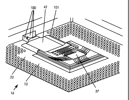
[0042] As another embodiment of the present invention,
the OHIC package 16 in figure 3e has been modified to
include precision cuts or walls in the housing that are
well located with respect to the positions of the solder
balls 101. The wall faces 100 on the housing, shown in
close-up in figure 3f, serve to internally reference the
12
CA 02635431 2008-06-09
WO 2006/060909 PCTlCA2005/001855
end-facet of the optical sub-assembly 14 shown in figure
8b. The dowel pins 120 from the optical sub-assembly 14 in
figures 8a and 8b are used to reference against the walls
of the housing and the end-facet 40 of the optical sub-
assembly is pushed up flush mating with the interior
alignment wall of the package housing. Figure 8b also shows
the positioning of a VCSEL 13 with respect to the optical
fibers 106 in their respective v-groove trenches 104. The
optical sub-assembly's internal features - the optical
fibers 106 in the v-groove trenches 104 of the optical
ferrule 42 - are thereby registered to the solder-balls 101
to correctly position the optical channels via these
internal mechanical alignment features.
[0043] The subsequent step of placing the completed
hybrid OHIC package 16 on a printed wiring board 20, and
solder-reflowing the package to align it to a pre-
positioned laminated optical waveguide 108, as shown in
figure 5c, is accomplished by the external alignment
features of the OHIC package housing. These features are
identical to the internal alignment features 100 that
aligned the optical, sub-assembly to the inside of the BGA
housing, but extend towards the exterior of the package 114
in order to accept the end-facet of the laminated optical
waveguide, as shown in figure 5c. The specific shape of the
laminated optical waveguide 108, shown in figure 5d, may
involve precision face-cuts, such as those possible with
precision laser machining, and- provide for side-walls or
angled walls 116 to be registered to the optical cores 57
of the optical waveguide. The end-facet of the laminated
optical waveguide can then be aligned to the features
13
CA 02635431 2008-06-09
WO 2006/060909 PCT/CA2005/001855
within the OHIC package 16 - figure 3g shows a perspective
view from below the printed wiring board where the printed
wiring board has been drawn as transparent. Before the
solder-reflow process attaching the OHIC package 16 to the
printed wiring board, the OHIC package 16 is mechanically
held against the angled walls 116 and side walls of the
laminated optical waveguide - thereby making the end-facet
of the laminated optical waveguide, and not the package's
solder balls, the TRI7Ts alignment feature for the OHIC=
package 16 on the printed wiring board. The end-facets and
the side-walls of the laminated optical waveguide 106 and
the end-facet of the optical ferrule 42 are pressed against
each other to accomplish optical alignment and then the
whole package is solder reflowed to permanently fix the
OHIC package 16 to the printed wiring board.
[0044] Once the OSA 14 has been placed inside the
recessed cavity 48 of the IC package 12 and has been
wirebonded to- the IC package 12, a new self-contained
optical multi-chip module is formed, called an optical
hybrid IC (OHIC) package 16. This OHIC package 16 can be
later on easily connected to a PWB 20 both electrically,
via the OHIC package's standard external connections 50,
and optically, via the optical facet 40 provided by the OSA
14.
[0045] The present invention therefore provides a, method
60 for creating an OHIC package 16. As illustrated in
Figure 6, the method 60 comprises providing an OSA 14 (step
61), wherein the OSA 14 has characteristics that were
mentioned earlier. Then the method 60 comprises providing
an IC package 12 (step 63). Then the method 60 comprises
14
CA 02635431 2008-06-09
WO 2006/060909 PCT/CA2005/001855
adapting the IC package 12 for accepting the OSA 14 (step
65). Then the method 60 comprises electrically bonding the
OSA 14 to the modified IC package 12 (step 67) in order to
obtain the OHIC package 16.
[0046] According to an embodiment, the OHIC package 16
has, on one of 'its sides, an optical facet 40 that is used
to couple light between an optical waveguide 18 of the PWB
20 and the optoelectronic device incorporated into the OHIC
16 package. Therefore, the present embodiment enables an
eventual optical side-coupling of 'an IC package 12 to an
optical waveguide 18.
[00471 In order to easily align the OHIC package 16 to
an optical waveguide, OHIC package 16 is provided with
external alignment features.
[00481 Thus the invention provides an OHIC package 16,
which is a self-contained hybrid semiconductor package that
has both electrical and optical inputs and outputs (I/O).
The electrical I/Os are accessed through typical means such
as pins, leads, or solder balls and the_ optical I/Os are
accessed by way, of a coupling out the side of the package
(side-coupling) via its optical facet 40. Also, as
mentioned earlier, the OHIC package 16 further has external
alignment features for easy optical coupling to an optical
waveguide.
[00491 Figure 8a shows an optical ferrule comprising a
plurality of optical fibers 106 embedded in a parallel
arrangement in a body 122 having a connector end 40, at
least two alignment V-grooves in the body at the connector
CA 02635431 2008-06-09
WO 2006/060909 PCT/CA2005/001855
end 130, at least two dowel pin V-grooves in the body at
the connector end, a cover member 122' having corresponding
opposite alignment and dowel pin V-grooves, at least two
alignment pins 120 bonded in the alignment V-grooves and
registering the cover member to the body correctly, the
alignment pins and the V-grooves being dimensioned such
that the location of the dowel pin V-grooves on both the
body and the cover member are located at the appropriate
position, wherein the flat abutment surface 134 can be
polished and dowel pins can be later inserted into the
dowel pin alignment V-grooves for guiding a complementary
ferrule member to end-couple fiber-to-fiber the plurality
of fibers at the connector end.
[0050] Figure 8b shows an assembly that can be treated
the same way as other packaged microchips (for example: the
placement of packaged chips on printed circuit boards) by
encapsulating the optoelectronic device to form a complete
package. However, the main reason for the requirement of a
flat, transparent window over the optoelectronic device
package is to provide the possibility for coupling other
optical devices (such as optical fibers) to the
optoelectronic device. The flat, transparent window 136
facilitates the alignment procedure used between the
optoelectronic device package and a secorid assembly (fiber
optic =ferrule, lens array, laser, etc.). The second
assembly can be placed on the flat surface and aligned to
the optoelectronic with a maximum of 3-degrees of movement
required (2-lateral and .1-rotational). This methodology is
known as stackable (or 2-D) optics, and greatly simplifies
the alignment procedure. A specific example of this
16
CA 02635431 2008-06-09
WO 2006/060909 PCT/CA2005/001855
alignment strategy involves a vertical cavity surface
emitting laser (VCSEL) array chip 13 with an array of
linear parallel optical fibers. Once the VCSEL array chip
has been encapsulated in a transparent resin, it has a
window (or flat, transparent surface) created above the
array of Lasers on the VCSEL chip. The surface is
essentially co-planar with the surface of the VCSEL chip.
The distance between the surface of the VCSEL chip and the
flat, transparent surface is kept to a minimum, without
exposing the VCSEL chip, so that a maximum amount, of
coupling into optical fibers is possible.
[0051] This arrangement offers several other beneficial
aspects as well. The encapsulated optoelectronic device is
hermetically sealed so that no moisture or contaminants can
develop over the device. It is also more resilient to
vibration, especially if wirebonding is used to connect to
the optoelectronic device. The transparent resin can also
reduce the divergence of the light emitted from the
optoelectronic device (assuming a high index of refraction
epoxy is used for the desired wavelength of light) and
thereby allow for a longer physical distance for the same
optical distance that the light can travel.
[0052] A method for manufacturing an encapsulated
optoelectronic package comprising an optoelectronic chip
will now be described. The method for manufacturing the
encapsulated optoelectronic package comprises providing a
substrate, securing an optoelectronic chip on the
substrate, providing a translucent coating substance over
the optoelectronic chip, and polishing the translucent
coating substance to create planar surface over at least
17
CA 02635431 2008-06-09
WO 2006/060909 PCT/CA2005/001855
the optoelectronic chip, substantially parallel to the
substrate, wherein the planar surface over the
optoelectronic chip provides an optical coupling window.
Optically enabled printed circuit board (OE-PCB)
S [0053] Figures 4a to 4e are examples of different
embodiments of the invention, where an OHIC package 16 has
been placed near an optical waveguide 18 that has been
fixed to a PWB 20, to form a so-called optically enabled
printed circuit board (OE-PCB). Figure 4a illustrates an
OHIC package 16 formed with a cavity up BGA 22 and an OSA
14. The optical output facet 40 is close to the end facet
21 of the optical waveguide 18 such that light between the
OHIC package 16 and the waveguide 18 is coupled. The,
optical output. facet 40 slightly extends beyond 53 the IC
package 12 to provide for an OHIC-waveguide external side-
coupling. Figure 4b illustrates an OHIC package 16, made
with a cavity down BGA 22, butt-coupled to an optical
waveguide 18, in a similar manner than in Figure 4a. Figure
4c shows an OHIC package 16 made with a cavity down PGA 26,
and butt-coupled to an optical waveguide 18, in a similar
manner to Figure 4a. Figure 4d is an example of an OHIC
package 16, this time made with a cavity down BGA 22, that
has an optical output facet 40 that is a recessed output
facet 52, enabling optical coupling with an optical
waveguide 18 that is slightly inserted in the side of the
OHIC package 16. Figure 4e is an example of an OHIC package
16, made with a cavity down BGA, coupled with an embedded
optical waveguide. All of these arrangements, and others
similar. and obvious to someone skilled in the art, are
1$
CA 02635431 2008-06-09
WO 2006/060909 PCT/CA2005/001855
possible realizations of the so-called optically enabled
printed circuit board (OE-PCB).
[0054] In some of the above embodiments, the optical
waveguide 18 of the PWB 20 is a planar laminated optical
waveguide. It will be obvious for someone skilled in the
art that other optical waveguide types could also be used,
all types of waveguides are thus included as possible
embodiments of the present invention including the use of
parallel ribbon optical fiber.
[0055] It is an objective of the present invention to
impact as little as possible the standard methods used to
build PWBs 20. To do so, a finished PWB 20 is augmented
with an external optical layer as shown in Figure 5a and 5b
to provide for a planar laminated optical waveguide 18 on
the surface of the PWB. It should be obvious to one skilled
in the art that an optical waveguide embedded in the-layers
of the PWB can also be used with the OHIC package 16 by
lowering the optical coupling facet 40 plane as shown in
figure 4e. However, given the objective to provide for non-
modified PWBs, the external , planar laminated optical
waveguide's layering structure can be used to facilitate
the vertical alignment between the optical coupling facet
40 of the OHIC package 16 and the cores 57 of the optical
waveguides 18. Figure 5a illustrates a end-facet 21 of a
multi-core planar laminated optical waveguide assembly 17
comprising: 1) an adhesive/alignment layer 79 of thickness
"A", 2) a buffer layer 59 of thickness "B minus A", 3) a
core 57 layer of thickness "C", and 4) a surrounding and
top cladding layer 58 of thickness "DN.
19
CA 02635431 2008-06-09
WO 2006/060909 PCT/CA2005/001855
[0056] In one embodiment of the present invention, a
vertical alignment between the optical coupling facet 40 of
the OHIC package 16 and the cores 57 of the optical
waveguides 18 is provided by a vertical alignment layer 45,
here the buffer layer 59, which allows to create optical
waveguides 18 that have cores 57 at a quite precisely known
vertical position with respect to-a vertical reference of
the PWB 20. The distributed thickness of the buffer layer
59 along the PWB 20 surface is such as to precisely follow
the thickness variations of the adhesive/alignment layer 79
along the PWB 20 surface to regulate the vertical height
'BN in figure 5a at a fixed distance between the cores 57
and the surface of the PWB 20. Methods known to someone
skilled in the art can be used to create a buffer layer 59
that will result in a substantially precise core 57
vertical position with respect to a PWB 20 reference
surface position.
[0057] In another embodiment of the present invention,
the vertical alignment between the optical coupling facet
40 of the OHIC package 16 and the cores 57 of the optical
waveguides 18 is provided by an alternate layer. This
alternate,layer is used as a vertical alignment reference
with respect to which an OHIC 16 package can be easily
coupled. For example, the cladding layer 58 can be the
vertical' alignment layer 45 and serve as a top surface
reference to which the. OHIC package 16 is aligned. In an
embodiment, the OHIC package's external alignment features
provide a vertical alignment by which a flat surface within
the OHIC package can rest on the top surface of the
cladding layer 58. The thickness "D" of the cladding layer
CA 02635431 2008-06-09
WO 2006/060909 PCT/CA2005/001855
58 down to the cores can then be maintained even if the
other thicknesses "A", "B", and "C" are not. Those are only
some arrangements of a plurality of 'arrangements provided
by the present invention.
[0058] The fully assembled OHIC package 16 is then
integrated with the planar laminated optical waveguide of
the PWB 20. The external alignment features within the body
of the OHIC package 16 are used to align the OSA's optical
facet 40 with the end-facet 21 of the optical waveguide 18.
As a person skilled in the art will appreciate, the
position and geometry of the optical waveguide 18 on the
PWB 20 instead of the electrical I{O pins (or leads or
solder balls) mostly determines the position of the OHIC
package 16. Similar to wirebonding as described above, the
"slack" provided by the standard electrical connections
(such as pins in plated through-holes of a printed circuit
board) can allow for small amounts of movement so that the
OSA 14 enclosed in the OHIC package 16 and the optical
waveguide interfaces can be aligned.
[0059] The main precision interface in this entire
assembly is the one between the OSA 14 found in the OHIC
package 16 and the optical waveguide 18. Given that the
optical waveguide 18 is appropriately dimensioned and
appropriately vertically positioned with respect to a PWB
20 surface reference (with the use of the vertical
alignment buffer layer technique described above) and the
OSA 14 is properly positioned inside the OHIC package, it
is the OHIC package 16 that becomes the common reference
and allows- the two optical interfaces (i.e. the optical
OHIC output facet 40 and the end facet 21 of the optical
21
CA 02635431 2008-06-09
WO 20N16/060909 PCT/CA2005/081855
waveguides 18) to become aligned. Thus, the present
invention takes advantage of the "slack" or "tolerance"
provided by standard electrical connection methods known to
one skilled in the art.
[0060] Turning now to Figure 7, the method 70 to provide
an optically enabled printed circuit board (OE-PCB) will be
summarized. The method comprises providing an OHIC package
16 (step 71). The method 70 also comprises providing a PWB
20 adapted to receive the OHIC package 16 and comprising at
.10 least one optical waveguide 18 (step 73) . The method 70
also comprises placing the OHIC package 16. on the PWB 20
and then bonding the OHIC package 16 to the PWB 20 (step
75). In step 77, an OE-PCB is obtained.
[0061] Although the present invention has been described
hereinabove by way of specific embodiments thereof, it can
be modified, without departing from the spirit and nature
of the subject invention as defined herein. The scope of
the invention is therefore intended to be limited solely by
the scope of the appended claims.
22