Note: Descriptions are shown in the official language in which they were submitted.
CA 02635535 2008-06-25
WO 2007/078941 PCT/US2006/048427
1
ILLUMINATION DEVICE
FIELD OF THE INVENTION
[0001] This invention relates to an illumination device including a
substantially planar
light-emitting surface coupled to an optical rod or optical taper.
BACKGROUND OF THE INVENTION
[0002] Advances in light source technology, such as, for example, light-
emitting diode
(LED) technology, have led to very bright and reliable solid state lamps.
However, challenges
remain with respect to coupling LEDs to optical transmission media, such as,
for example,
optical rods and optical tapers. While there have been numerous attempts to
utilize low power
(<1W electrical power consumption, typically operating below 100mW) light-
emitting diodes
(LEDs) coupled to fiber optic light guides or other optical devices as light
sources for
endoscopy, dentistry, and for remote illumination of objects (as with a
flashlight, head light, or
lamp), most of these prior attempts have employed numerous low power LEDs for
remote
illumination. Generally, multiple LEDs are necessary because the light output
from a single, low
power LED is typically too weak to properly illuminate an object. In addition,
the arrangement
of the multiple LEDs to the optical transmission media used in these prior
attempts has resulted
in unacceptable light loss, thereby further decreasing the low power LED's
ability to properly
illuminate an object.
SUMMARY OF THE INVENTION
[0003] In general, the present invention relates to increasing the amount
of light
transmitted through an illumination device by means of an inventive coupling
approach between
a light source and an optical rod or optical taper. In some embodiments, the
invention further
relates to an endoscope (e.g., medical or industrial) including the inventive
coupling approach, a
lamp including the inventive coupling approach, or a head light including the
inventive coupling
CA 02635535 2008-06-25
WO 2007/078941 PCT/US2006/048427
-2-
approach. Certain embodiments of the present invention, utilize a high power
LED, (i.e., an
LED having a power consumption between about I to 5W).
190041 In one aspect, the invention relates to an illumination device,
such as, for
example, an endoscope, a lamp, or a head light. The illumination device
includes a light source
including a substantially planar light-emitting surface and an optical rod or
optical taper disposed
proximate to the substantially planar light-emitting surface. By arranging the
optical rod or
optical taper in a proximate relationship to the substantially planar light-
emitting surface, the two
elements are coupled in a manner which allows a large amount of the light
emitted by the light
source to be transmitted directly into the optical rod or optical taper. As a
result, a greater
amount of light from the light source can be transmitted through the
illumination device and onto
an object for illumination. Embodiments of the present invention do not
include auxiliary optics,
such as lenses or mirrors, disposed between the light source and the optical
rod or optical taper,
but instead rely on the close placement (e.g., direct contact or close
proximity) of the optical rod
or taper to the planar light-emitting region of the light source. The lack of
auxiliary optics
between the light source and the optical rod or optical taper simplifies the
mechanical design and
space requirements for the illumination device. As a result, illumination
devices in accordance
with the present invention can be small and compact while providing the
desired illumination
strength.
[0005] Embodiments of this aspect of the invention can include one or more
of the
following features. The substantially planar light-emitting surface can
include an emitting
surface of a light-emitting diode chip. In some embodiments, the substantially
planar light-
emitting surface can include the surface of a light-emitting diode chip that
has been coated with a
film of a substance that emits light when the light-emitting diode chip is
activated (e.g., a
phosphor film coating the surface of the chip). In certain embodiments, the
substantially planar
light-emitting surface comprises a transparent substantially planar window
disposed over an
CA 02635535 2008-06-25
WO 2007/078941 PCT/US2006/048427
-3-
emitting surface of a light emitting diode chip. For example, in some
embodiments, the window
can be disposed directly over a LED chip. In other embodiments, the window can
be disposed
over a phosphor coated LED chip. The substantially planar light-emitting
surface can be in
direct contact with the optical rod or optical taper. In some embodiments an
adhesive or index
matching material (e.g., a coupling gel) can be disposed between the optical
rod or optical taper
and the substantially planar light-emitting surface. In certain embodiments,
the optical rod or
taper is disposed proximate to but not in direct contact with the
substantially planar light-
emitting surface. As a result, a gas is disposed between the optical rod or
optical taper and the
substantially planar light-emitting surface.
[0006] Other embodiments of this aspect of the invention can include one
or more of the
following features. The optical rod can be formed of a clad rod, a silvered
rod, an aluminized
rod, or a fiber bundle. The optical rod can have a first end that is proximate
to the substantially
planar light-emitting surface and a second end that is proximate to a light
guide. The optical
taper can include a first end that has a smaller surface area than a second
end of the optical taper.
In some embodiments, the first end (i.e., with the smaller surface area) can
be in direct contact
with the substantially planar light-emitting surface of the light source. In
other embodiments, the
second end (i.e., with the larger surface area) can be in direct contact with
the substantially
planar light-emitting surface of the light source. The optical taper can be
formed of a glass
optical taper, a plastic optical taper, or a plurality of fibers. While one
end of the optical rod or
optical taper is proximate to the substantially planar light-emitting surface,
the other end of the
optical rod or taper can be connected to a light guide. In some embodiments, a
light post taper
can be disposed between the optical rod or the optical taper and the light
guide.
[00071 In another aspect, the invention is directed to a method of
collimating light from a
light source. The method includes attaching an optical rod or optical taper to
a substantially
planar light-emitting surface of the light source and activating the light
source.
CA 02635535 2012-08-14
- 4 -
[0008] In another aspect, the invention is directed to a method of
illuminating an object.
The method includes providing a device including a light source having a
substantially planar
light-emitting surface and an optical rod or taper having a first end held
proximate to the
substantially planar light-emitting surface; positioning the device relative
to the object; and
activating the light source. In some embodiments, the optical rod or taper can
include a second
end attached to optics to transmit the light emitted from the light source
through the optical rod
or taper to the object.
[0008a] In a further aspect, the present invention provides an
illumination device
comprising: a light source including a substantially planar light-emitting
surface, an optical taper
including a light receiving end and a second end, the light receiving end
having a smaller surface
area than the second end and the light receiving end matching an area of the
substantially planar
light-emitting surface; and a light post taper; wherein the light receiving
end of the optical taper is
disposed proximate to the substantially planar light-emitting surface to
optically couple the optical
taper and the substantially planar light-emitting surface, and the second end
of the optical taper is
proximate to the light post taper.
[0009] Any of the above implementations can realize one or more of the
following
advantages. The illumination devices and methods described above are efficient
at transmitting
light from the light source into the optical rod or optical taper. As a
result, objects can be
illuminated with a proper amount of light (e.g., object is visible under
endoscopic examination;
object under a lamp is sufficiently lighted for viewing purposes). Another
advantage realized in
the above embodiments is that the optical rod or optical taper can be coupled
to the light source
without the use of additional optical components or auxiliary optics, such as,
for example,
mirrors, lenses, reflectors. As a result, a large amount of the light emitted
by the light source can
be coupled directly into the optical rod or optical taper, thereby allowing a
greater amount of
light from the light source to be transmitted to the objects under
investigation. The lack of
auxiliary optics between the light source and the optical rod or taper also
simplifies the
CA 02635535 2012-08-14
- 4a -
mechanical design and size of the illumination device. In addition, the high
light output and high
coupling efficiency of the light emitted by the light source into the optical
rod or optical taper
increases battery lifetime and thus permits the use of smaller capacity, and
smaller volume
batteries to power the illumination device.
CA 02635535 2008-06-25
WO 2007/078941 PCT/US2006/048427
-5-
BRIEF DESCRIPTION OF THE DRAWINGS
[0010] The foregoing and other features and advantages of the present
invention, as well
as the invention itself, will be more fully understood from the following
description of various
embodiments, when read together with the accompanying drawings.
[0011] FIG. I is an illustration of a prior art illumination device
including a LED-based
light source.
[0012] FIG. 2 is an illustration of an illumination device including a
substantially planar
light-emitting surface in accordance with the present invention.
[0013] FIG. 3 is an illustration of another embodiment of an illumination
device
including a substantially planar light-emitting surface in accordance with the
present invention.
[0014] FIG. 4 is an illustration of another embodiment of an illumination
device
including a substantially planar light-emitting surface in accordance with the
present invention.
[0015] FIG. 5 is an illustration of another embodiment of an illumination
device
including a substantially planar light-emitting surface in accordance with the
present invention.
[0016] FIG. 6 is an illustration of another embodiment of an illumination
device
including a substantially planar light-emitting surface in accordance with the
present invention.
[0017] FIG. 7 is an illustration of the illumination device of FIG. 6
disposed within a
handle of an endoscope.
[0018] FIG. 8 is an illustration of another embodiment of an illumination
device
including a substantially planar light-emitting surface in accordance with the
present invention.
CA 02635535 2008-06-25
WO 2007/078941 PCT/US2006/048427
L6-
DETAILED DESCRIPTION
[0019] Prior art illumination devices, such as, for example; the
illumination device
shown in FIG. 1, include a light source 5 having a dome-shaped lens 10
optically coupled to
transmission media 15. With this coupling arrangement, light is ineffectively
transmitted to the
transmission media 15 because the light emitting portion 20 of the light
source 5 is not
sufficiently close to the transmission media 15 (i.e., due to the curvature of
the dome lens 10, the
light emitting portion 20 is spaced at an unacceptable distance away from the
transmission
media). In addition, the dome shape lens 10 provides a convex light-emitting
surface. As a
result, a portion of the light passing through an interface between the light
source 5 and the
transmission media 15 is lost, thereby decreasing the light strength and
efficiency of
conventional illumination devices.
[0020] Illumination devices of the present invention include a
substantially planar light-
emitting surface which is proximate to either an optical rod or an optical
taper. As a result, a
greater amount of light is transmitted from the light source to the optical
rod or taper than in
prior art systems.
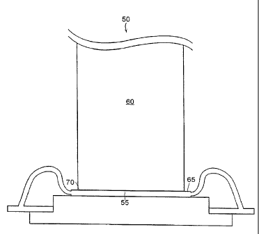
[0021] In accordance with one embodiment of the invention, an illumination
device 50
shown in FIG. 2 includes a LED 55, such as, for example, a high power LED
(Luxeon III Model
LXHL-LW3C, Lumileds Lighting, San Jose, CA) and an optical rod 60. A dome
lens, such as
the dome lens 10 shown in FIG. 1, and any index matching material surrounding
the LED 55 was
not employed or was removed prior to coupling the LED 55 to the optical rod
60. As a result,
the substantially planar light-emitting surface 65 of the LED 55 (e.g., the
surface of a light-
emitting chip in the LED 55) is proximate to a first end 70 of the optical rod
60. The
substantially planar light-emitting surface 65 and the first end 70 together
form a planar interface
in which light can be transmitted with less light loss than in an interface
including a curved or
convex surface.
CA 02635535 2008-06-25
WO 2007/078941 PCT/US2006/048427
-7-
[0022] The coupling arrangement of the light source 55 and the optical rod
60 provides
many advantages to the illumination device 50 over prior art systems. Besides
an increase in the
amount of light transmitted through the illumination device, the coupling
arrangement shown in
FIG. 2 provides light source protection and mechanical stability to the
illumination device 50.
Specifically, the optical rod 60 protects the LED 55 from the external
environment and also
provides an additional advantage of being a rugged element to which additional
elements of the
illumination device can be easily coupled to. For example, referring to FIG.
3, a light guide
bundle 80 formed of a plurality of optical fibers and held together by a
ferrule 85 can easily be
attached to the optical rod 60 without fear of damaging the light-emitting
diode.
[0023] The substantially planar light-emitting surface 65 of the LED 55 is
the top surface
of the LED chip. In some embodiments, the substantially planar light-emitting
surface 65 can
further include a coating of a substance that emits white light or one or more
specific colors of
light when activated. For example, the substantially planar light-emitting
surface 65, in certain
embodiments, includes a phosphor film or coating on the top surface of the LED
55. In other
embodiments, such as the embodiments shown in FIG. 4, the substantially planar
light-emitting
surface 65 can be formed of a transparent flat window placed over the LED 55.
In this
embodiment, light is emitted from the top surface of the LED 55 and then
through the
transparent window. The flat window is proximate to the optical rod 60 and
forms a planar
=
interface with the optical rod.
[0024] Optical rod 60 can be formed from a transparent material or any
material which
allows light to pass through. Examples of materials that can be used to form
the optical rod
include glass, plastic, and sapphire. In addition, the optical rod can be a
clad rod, a silvered rod,
an aluminized rod, or formed form a plurality of fibers (e.g., fiber bundle).
[0025] Referring to FIG. 5, illumination device 150 includes LED 55 and an
optical taper
160 positioned proximate to the substantially planar light-emitting surface 65
of the LED 55.
CA 02635535 2008-06-25
WO 2007/078941 PCT/US2006/048427
-8-
Optical taper 160 is formed from any transparent material such as, for
example, glass or plastic
and has a first end or a smaller surface area end 162 and a second end or a
larger surface area end
164. The optical taper 160 can be made from a solid rod of transparent
material that is drawn
down to a smaller diameter or profile at one end or, in other embodiments, the
optical taper can
be formed from a plurality of fibers (e.g., a fiber taper) that are also drawn
down in diameter or
profile. The optical taper 160 provides the advantage of resizing and
reshaping the output of the
light from the light source (e.g., LED 55). For example, a typical LED die is
about lmm x 1mm
square that emits over a broad angular cone. Employing a high index of
refraction transparent
material, such as, for example glass or plastic, in the taper 160 produces a
high acceptance angle
of light at the first end or smaller surface area end 162 of the taper. The
larger surface area end
164 of the taper exhibits a reduction in the numerical aperture (NA) by the
ratio of the end
diameters. For example, a 1:3 taper made from glass has an angular aperture at
the first end 162
of 123 degrees and a numerical aperture of 0.88 NA. The second end 164 of the
taper has a
numerical aperture of 0.29 NA and an angular aperture of 34 degrees. As a
result, the taper 160
provides a number of advantages to the illumination device 150. For example,
in the
embodiment shown in FIG. 5, the taper 160 collects a very large solid angle of
light emitted by
the LED 55 because of the high NA at the first end 162 of the taper. The taper
160 protects the
LED 55 from the environment. The taper 160 collimates the light as it passes
through the taper
160 and delivers the light in a manner that is more readily coupled to light
guides. The taper 160
presents a lower dispersion of light to additional optics should imaging or
collection of the light
be necessary for a particular application, such as, for example, spot light
imaging in a museum or
projection of a transparency image. In addition, the taper 160 provides
mechanical stability to
illumination device 150 and is a rugged element to which additional elements
of the illumination
device can be easily coupled to.
CA 02635535 2008-06-25
WO 2007/078941 PCT/US2006/048427
-9-
[0026] While the taper 160 as shown in FIG. 5 has its first end 162 in
direct contact with
the LED 55, other resizing and reshaping arrangements are available. For
example, instead of
the small surface area end 162 being in contact with the planar light-emitting
surface 65 of the
LED 55, the larger surface area 164 can be in contact with the light-emitting
surface 65. This
embodiment allows for a smaller angle of light to be collected from the LED
but provides a
greater dispersion of light emitted from the taper 160.
[0027] Referring to FIG. 6, the illumination device 150 can be combined
with a light
guide bundle 200 including a light post taper 210. The illumination device 150
can be used as
the light source for an endoscope. The light from the LED 55 is emitted
through the illumination
device 150 and is collected by the light post taper 210, which is adhered to
the fiber optic light
guide bundle 200. The light guide bundle 200 transmits the light to a remote
location, such as,
for example, through the body of the endoscope to illuminate an object under
inspection. In
general, the light post taper 210 selected for use with the illumination
device 150 and the light
guide bundle 200 has a first end or light receiving end 215 that has a surface
area size
comparable to the second end of the taper 160 and a second end or a light
transmitting end 220
that has a surface area size comparable to the size of the connection end 230
of the light guide
bundle 200.
[0028] In certain embodiments, the illumination device 150 can be
positioned within a
housing. Referring to FIG. 7, illumination device 150 is within a detachable
light source housing
300 including a connector 310 to couple the illumination device 150 to a light
guide post taper '
210 surrounded by a light post 250. The illumination device 150, including the
LED 55 having a
light-emitting surface 65 proximate to taper 160, is inserted into a recess
within the detachable
housing 300. The light post 250 mates with one end of the detachable housing
so that the light
post taper 210 comes into direct contact with the taper 160 of the
illumination device.
CA 02635535 2008-06-25
WO 2007/078941 PCT/US2006/048427
-10-
E0029] The optical taper 160 and the light post taper 210 can be selected
for use with the
illumination device 150 to increase the amount of light transmitted from the
illumination device
into the light guide bundle 200. For example, in an embodiment in which the
optical taper 160
has a 1:3 ratio of end areas, with the small surface area end 162 having a 1.0
NA and a large
surface area end 164 having a 0.33 NA, the collection angle at the small
surface area end 162 is
180 degrees. The 1:3 ratio of end diameters cause the output NA to decrease to
0.33. In other
words, the light exiting the larger surface area end 164 has an angular
aperture of approximately
39 degrees. As a result, the light initially emitted by the LED 55 over the
180 degrees exits the
taper 160 contained in a 39 degree cone at the larger surface area end 164. In
the present
embodiment, the light post taper 210 located proximate to the larger surface
area end 164 is
made of 0.66 NA glass and has a 2:1 diameter ratio. As a result, the larger
surface area end 215
of the light post taper 210 receives light over about a 39 degree angle, a
near perfect match to the
light transmitted from the larger surface area end 164 of the optical taper
160. The light entering
the light post taper 210 is reduced in diameter by a factor of 2, with a
resulting increase in
numerical aperture to 0.66 NA and an exit cone angle of 83 degrees for the
light exiting the
smaller surface area end 220 of the light post taper 210. Adhered directly to
the smaller surface
area end 220 of the light post taper 210 is the light guide bundle 200 formed
of 0.66 NA glass,
which has an acceptance angle (e.g., 83 degrees) that substantially matches
the exit angle of the
light post taper 210 (e.g., 83 degrees).
[0030] The illumination devices described above can be used to illuminate
objects. For
example, by utilizing either device 50 or 150, light from a light source can
be collimated and
transmitted to illuminate an object. Specifically, by coupling an optical rod
or optical taper to a
substantially planar light-emitting surface of an LED and activating the LED,
the light generated
and dispersed by the LED is collimated and transmitted through the optical rod
and taper to
produce a collimated light beam that can illuminate objects. In certain
embodiments, the device
CA 02635535 2008-06-25
WO 2007/078941 PCT/US2006/048427
-11-
50 or 150 can be disposed within a lamp. When the lamp is positioned relative
to an object and
the light source 55 within the lamp is activated, the lamp produces a spot
light which illuminates
the object.
[0031] While certain embodiments have been described, other embodiments
are also
possible. As an example, while LED 55 has been described as a chip 55 free
from or removed
completely from a dome lens, in some embodiments, such as the embodiment shown
in FIG 8,
the LED 55 can remain in a modified or partially removed dome lens.
Specifically, the dome
lens 10 surrounding the LED 55 can be ground and polished nearly down to the
level of the
encapsulent-LED interface, so as to preserve the integrity of the mechanical
package of the LED
chip. After the dome lens has been partially removed, the planar light-
emitting surface 65 of the
LED 55 is accessible for connection to an end of the optical rod 60 or optical
taper 160. To
couple the optical rod or taper to the substantially planar light-emitting
surface, a manufacturer
positions an end of the rod or taper in a proximate relationship to the light-
emitting surface 65.
This process entails positioning the optical rod or taper as close as possible
to the light-emitting
surface 65 without damaging the light-emitting qualities of the LED 55_ For
example, in certain
embodiments, the end of the rod or taper is in direct physical contact with
the surface 65. In
other embodiments, the end of the rod or taper is spaced a distance less than
about 1 to 2
millimeters away from the surface 65. As a result, air, gas, adhesive, or an
index matching
material, such as, for example, a coupling gel may be disposed between the
surface 65 and the
end of the rod or taper within the 1 to 2 millimeter gap.
[0032] Variations, modifications, and other implementations of what is
described herein
will occur to those of ordinary skill without departing from the spirit and
the scope of the
invention. Accordingly, the invention is not to be defined only by the
preceding illustrative
description.