Note: Descriptions are shown in the official language in which they were submitted.
CA 02635668 2008-06-27
WO 2007/075937 PCT/US2006/048878
1
PROCESS OF MAKING ELECTROLESSLY PLATED
AUTO-CALIBRATION CIRCUITS FOR TEST SENSORS
FIELD OF THE INVENTION
10011 The present invention generally relates to a process of making auto-
calibration circuits for test sensors. More specifically, the process is
directed to making
electroless auto-calibration circuits for test sensors that are adapted to be
used in calibrating
instruments or meters that determine the concentration of an analyte (e.g.,
glucose) in a fluid.
BACKGROUND OF THE INVENTION
[002] The quantitative determination of analytes in body fluids is of great
importance in the diagnoses and maintenance of certairi physiological
abnormalities. For
example, lactate, cholesterol and bilirubin should be monitored in certain
individuals. In
particular, it is important that diabetic individuals frequently check the
glucose level in their
body fluids to regulate the glucose intake in their diets. The results of such
tests can be used
to determine what, if any, insulin or other medication needs to be
administered. In one type
of blood-glucose testing system, sensors are used to test a sample of blood.
10031 A test sensor contains biosensing or reagent material that reacts with
blood
glucose. The testing end of the sensor is adapted to be placed into the fluid
being tested, for
example, blood that has accumulated on a person's finger after the finger has
been pricked.
The fluid is drawn into a capillary channel that extends in the sensor from
the testing end to
the reagent material by capillary action so that a sufficient amount of fluid
to be tested is
drawn into the sensor. The fluid then chemically reacts with the reagent
material in the
sensor resulting in an electrical signal indicative of the glucose level in
the fluid being tested.
This signal is supplied to the meter via contact areas located near the rear
or contact end of
the sensor and becomes the measured output.
[004) Diagnostic systems, such as blood-glucose testing systems, typically
calculate the actual glucose value based on a measured output and the known
reactivity of the
reagent-sensing element (test sensor) used to perform the test. The reactivity
or lot-
calibration information of the test-sensor may be given to the user in several
forms including
a number or character that they enter into the instrument. One prior art
method included
using an element that is similar to a test sensor, but which was capable of
being recognized as
a calibration element,by the instrument. The test,element'.s.
informatio..n..is read, by the,,
CA 02635668 2008-06-27
WO 2007/075937 PCT/US2006/048878
2
instrument or a memory element that is plugged into the instrument's
microprocessor board
for directly reading the test element.
[005] These methods suffer from the disadvantage of relying on the user to
enter
the calibration information, which some users may not do. In this event, the
test sensor may
use the wrong calibration information and thus return an erroneous result.
Improved systems
use an auto-calibration circuit that is associated with the sensor package.
The auto-calibration
circuit is read automatically when the sensor package is placed in the meter
and requires no
user intervention.
[0061 One method of currently forming a metallic auto-calibration circuit is
by
laminating a substrate with a metal foil followed by a subtractive etching
process to define the
electrical connections. This process tends to be more costly than necessary
because a portion
of the metallic material is removed from the substrate and, thus, is not
present in finalized
auto-calibration circuit.
[007] It would be desirable to provide a method for forming an auto-
calibration
circuit that is more cost-effective than existing processes, while still being
an efficient
process.
SUMMARY OF THE INVENTION
[008] According to one method, an auto-calibration circuit to be used with a
sensor package is formed. The sensor package includes at least one test sensor
and is adapted
to be used with an instrument or meter. A substrate is provided. Catalytic ink
or catalytic
polymeric solution is applied to at least one side of the substrate. The
catalytic ink or
catalytic polymeric solution is used to assist in defining the electrical
connections on the
substrate. The substrate is electrolessly plated where the catalytic ink or
catalytic polymeric
solution was applied to form the electrical connections of the substrate. The
electrical
connections convey. auto-calibration information for the at least one test
sensor to the
instrument.
[009] According to another method, an auto-calibration circuit to be used with
a
sensor package is formed. The sensor package includes at least one test sensor
and is adapted
to be used with an instrument or meter. A substrate is provided. At least one
aperture is
formed through the substrate. Catalytic ink or catalytic polymeric solution is
applied to two
opposing sides of the substrate. The catalytic ink or catalytic polymeric
solution is used to
CA 02635668 2008-06-27
WO 2007/075937 PCT/US2006/048878
3
assist in defining the electrical connections on the substrate. The substrate
is electrolessly
plated where the catalytic ink or catalytic polymeric solution was applied to
form the
electrical connections of the substrate. The electrical connections convey
auto-calibration
information for the at least one test sensor to the instrument.
[010) According to a further method, a sensor package is formed that is
adapted
to be used with at least one instrument in determining an analyte
concentration in a fluid
sample. A substrate is provided. Catalytic ink or catalytic polymeric solution
is applied to at
least one side of the substrate. The catalytic ink or catalytic polymeric
solution is used to
assist in defining the electrical connections on the substrate. The substrate
is electrolessly
plated where the catalytic ink or catalytic polymeric solution was applied to
form the
electrical connections of the substrate. The electrical connections convey
auto-calibration
information for the at least one test sensor to the instrument. The auto-
calibration circuit is
attached to a surface of a sensor-package base. At least one test sensor is
adapted to receive
the fluid sample and is operable with at least one instrument is provided.
BRIEF DESCRIPTION OF THE DRAWINGS
[0111 FIG. 1 is a top perspective view of a sensing instrument according to
one
embodiment.
[012] FIG. 2 is the top perspective view of an interior of the sensing
instrument
of FIG. 1.
[013] FIG. 3 is a sensor package according to one embodiment for use with the
sensing instrument of FIGs. 1 and 2.
[014] FIG. 4 is a top view of an auto-calibration circuit or label formed by
one
method of the present invention.
[015] FIG. 5 is a top view of the auto-calibration circuit of FIG. 4 according
to
one pattern.
[016] FIG. 6 is a top view of an auto-calibration circuit formed by another
method of the present invention.
[017] FIG. 7 is a top view of an auto-calibration circuit of FIG. 6 according
to
one pattern.
[018] FIG. 8a is a top perspective view of a substrate that is used to forrn
the
auto-calibration circuit of FIG. 4 according to one process.
CA 02635668 2008-06-27
WO 2007/075937 PCT/US2006/048878
4
[019] FIG. 8b is the substrate of FIG. 8a with catalytic ink or catalytic
polymeric
solution being added thereto according to one process.
[020] FIG. 8c is the substrate with the catalytic ink or catalytic polymeric
solution of FIG. 8b being exposed to ultraviolet light.
[021] FIG. 8d is a side view of a bath that is adapted to electrolessly plate
the
substrate with an electroless plated solution after being exposed to the
ultraviolet light of FIG.
8c.
[022) FIG. 9a is a top perspective view of a substrate that is used to form an
auto-calibration circuit according to another process.
[023] FIG. 9b is the substrate of FIG. 9a with a plurality of apertures formed
therein.
[024] FIG. 9c is a top perspective view of the substrate of FIG. 9b with
catalytic
ink or catalytic polymeric solution being added thereto.
[025] FIG. 9d is a bottom perspective view of the substrate of FIG. 9b with
catalytic ink or catalytic polymeric solution being added thereto.
10261 FIG. 9e is a top perspective view of the substrate with the catalytic
ink or
catalytic polymeric solution of FIGs. 9c, 9d being exposed to ultraviolet
light.
[027] FIG. 9f is a bath that is adapted to electrolessly plate the substrate
with an
electroless plated solution after being exposed to ultraviolet light of FIG.
9e.
[028] FIG. l0a is an enlarged side view of an aperture depicted in FIG. 9b
after
catalytic ink or catalytic polymeric solution has been applied to the
substrate.
[029] FIG. 1 Ob is an enlarged side view of the aperture depicted in FIG. l0a
after
the substrate has been electrolessly plated.
DETAILED DESCRIPTION OF ILLUSTRATED EMBODIMENTS
[030] An instrument or meter in one embodiment uses a test sensor adapted to
receive a fluid sample to be analyzed, and a processor adapted to perform a
predefined test
sequence for measuring a predefined parameter value. A memory is coupled to
the processor
for storing predefined parameter data values. Calibration information
associated with the test
sensor may be read by the processor before the fluid sample to be measured is
received.
Calibration information may be read by the processor after the fluid sample to
be measured is
received, but not after the concentration of the analyte has been determined.
Calibration
CA 02635668 2008-06-27
WO 2007/075937 PCT/US2006/048878
information is used in measuring the predefined parameter data value to
compensate for
different characteristics of test sensors, which will vary on a batch-to-batch
basis. Variations
of this process will be apparent to those of ordinary skill in the art from
the teachings
disclosed herein, including but not limited to, the drawings.
[031] Referring now to FIGs. 1-3, an instrument or meter 10 is illustrated. In
FIG. 2, the inside of the instrument 10 is shown in the absence of a sensor
package. One
example of a seinsor package (sensor package 12) is separately illustrated in
FIG. 3. Referring
back to FIG. 2, a base member 14 of the instrument 10 supports an auto-
calibration plate 16
and a predetermined number of auto-calibration pins 18. As shown in FIG. 2,
for example,
the instrument 10 includes ten auto-calibration pins 18. It is contemplated
that the number of
auto-calibration pins may vary in number and shape from that shown in FIG. 2.
The auto-
calibration pins 18 are connected for engagement with the sensor package 12.
[032] The sensor package 12 of FIG. 3 includes an auto-calibration circuit or
label 20, a plurality of test sensors 22, and a sensor-package base 26. The
plurality of test
sensors 22 is used to determine concentrations of analytes. Analytes that may
be measured
include glucose, lipid profiles (e.g., cholesterol, triglycerides, LDL and
HDL), microalbumin,
hemoglobin Alo, fiuctose, lactate, or bilirubin. It is contemplated that other
analyte
concentrations may be determined. The analytes may be in, for example, a whole
blood
sample, a blood serum sample, a blood plasma sample, other body fluids like
ISF (interstitial
fluid) and. urine, and non-body fluids. As used within this application, the
term
"concentration" refers to an analyte concentration, activity (e.g., enzymes
and electrolytes),
titers (e.g., antibodies), or any other measure concentration used to measure
the desired
analyte.
[033] In one embodiment, the plurality of test sensors 22 includes an
appropriately selected enzyme to react with the desired analyte or analytes to
be tested. An
enzyme that may be used to react with glucose is glucose oxidase. It is
contemplated that
other enzymes may be used such as glucose dehydrogenase. An example of a test
sensor is
disclosed in U.S. Patent No. 6,531,040 assigned to Bayer Corporation_ It is
contemplated that
other test sensors may be used.
[034] Calibration information or codes assigned for use in the clinical value
computations to compensate for manufacturing variations between sensor lots
are encoded on
the auto-calibration circuit 20. The auto-calibration circuit 20 is used to
automate the process
CA 02635668 2008-06-27
WO 2007/075937 PCT/US2006/048878
6
of transferring calibration information (e.g., the lot specific reagent
calibration information
for the plurality of test sensors 22) such that the sensors 22 may be used
with at least one
instrument or meter. In one embodiment, the auto-calibration circuit 20 is
adapted to be used
with different instruments or meters. The auto-calibration pins 18
electrically couple with the
auto-calibration circuit 20 when a cover 38 of the instrument 10 is closed and
the circuit 20 is
present. The auto-calibration circuit 20 will be discussed in detail in
connection with FIG. 4.
[0351 According to one method, an analyte concentration of a fluid sample is
determined using electrical current readings and at least one equation. In
this method,
equation constants are identified using the calibration information or codes
from the auto-
calibration circuit 20. These constants may be identified by (a) using an
algorithm to
calculate the equation constants or (b) retrieving. the equation constants
from a lookup table
for a particular predefined calibration code that is=read from the auto-
calibration circuit 20.
The auto-calibration circuit 20 may be implemented by digital or analog
techniques. In a
digital implementation, the instrument assists in determining whether there is
conductance
along selected locations to determine the calibration information. In an
analog
implementation, the instrument assists in measuring the resistance along
selected locations to
detennine the calibration information. -
[036] Referring back to FIG. 3, the plurality of test sensors 22 is arranged
around
the auto-calibration circuit 20 and extends radially from the area containing
the circuit 20.
= The plurality of sensors 22 of FIG. 3 is stored in individual cavities or
blisters 24 and read by
associated sensor electronic circuitry before one of the plurality of test
sensors 22 is used.
The plurality of sensor cavities or blisters 24 extends toward a peripheral
edge of the sensor
package 12. In this embodiment, each sensor cavity 24 accommodates one of the
plurality of
test sensors 22.
[037] The sensor package 12 of FIG. 3 is generally circular in shape with the
sensor cavities 24 extending from near the outer peripheral edge toward and
spaced apart
from the center of the sensor package 12. It is contemplated, however, that
the sensor
package may be of different shapes then depicted in FIG. 3. For example, the
sensor package
may be a square, rectangle, other polygonal shapes, or non-polygonal shapes
including oval.
[038] With reference to FIG. 4, the auto-calibration circuit 20 in this
embodiment is adapted to be used with (a) the instrument or meter 10, (b) a
second
instrument or meter (not shown) being distinct or different from the
instrument 10, and (c) the
CA 02635668 2008-06-27
WO 2007/075937 PCT/US2006/048878
7
plurality of sensors 22 operable with both the instrument 10 and the second
instrument. Thus,
in this embodiment, the auto-calibration circuit 20 may be considered as
"backwards"
compatible because it is adapted to be used with the second instrument (i.e.,
a new
instrument) and the first instrument (i.e., an older instrument). The auto-
calibration circuit
may be used to work with two older instruments or two newer instruments. To
reduce or
avoid manufacturing modifications, it is desirable for a "backwards"
compatible auto-
calibration circuit not to increase the size of the circuit or decrease the
size of the electrical
contact areas. In another embodiment that will be discussed below in
connection with FIGs.
6 and 7, an auto-calibration circuit is adapted to be used with one
instrument.
[039] According to one embodiment, the sensor package contains a plurality of
sensors operable with at least one instrument (e.g., sensor package 12
containing a plurality of
sensors 22 operable with the instrument 10 and the second instrument). When
the plurality of
sensors 22 has essentially the same calibration characteristics, calibrating
the instrument 10
for one of the sensors 22 is effective to calibrate the instrument 10 for each
of the plurality of
sensors 22 in that particular package 12.
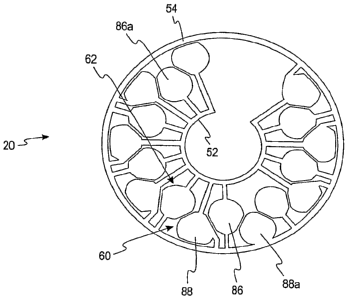
[040] The auto-calibration circuit 20 of FIG. 4 includes an inner ring 52, an
outer
ring 54, a plurality of electrical connections 60, and a plurality of
electrical connections 62
distinct from the plurality of electrical connections 60. For some
applications, the inner ring
52 represents logical Os and the outer ring 54 represents logical ls. It is
contemplated that the
inner ring or the outer ring may not be continuous. For example, the inner
ring 52 is not
continuous because it does not extend to form a complete circle. The outer
ring 54, on the
other hand, is continuous. The inner ring and the outer ring may both be
continuous and in
another embodiment the inner ring and the outer ring are not continuous. It is
contemplated
that the inner ring and outer rings may be shapes other than circular. Thus,
the teml "ring" as
used herein includes non-continuous structures and shapes other than circular.
[041] The plurality of electrical connections 60 includes a plurality of outer
contact areas 88 (e.g., contact pads). The plurality of outer contact areas 88
is radially
positioned around the circumference of the auto-calibration circuit 20. The
plurality of
electrical connections 62 includes a plurality of inner contact areas 86. The
inner contact
areas 86 are positioned closed to the center of the circuit 20 than the outer
contact areas 88. It
is contemplated that the plurality of outer contact areas and the inner
contact areas may be
located in different positions than. depicted in FIG. 4.
CA 02635668 2008-06-27
WO 2007/075937 PCT/US2006/048878
8
10421 The plurality of electrical connections 62 is distinct from the
plurality of
electrical connections 60. It will be understood, however, that use of the
term "distinct" in
this context may only mean that the encoded information is distinct, but the
decoded
information is essentially the same. For example, the instrument 10 may have
essentially the
same calibration characteristics, but the contacts, e.g., pins 18, to couple
with the encoded-
calibration information are located in different places for each instrument.
Accordingly, the
encoded-calibration information of the first and second instruments
corresponding to each
instrument is distinct because the encoded information must be arranged to
couple with the
appropriate instrument.
[043] In the embodiment depicted in FIG. 4, the plurality of electrical
connections 60 is adapted to be routed directly from each of the plurality of
outer contact
areas 88 to a respective first common connection (e.g., inner ring 52) or a
second common
connection -(e.g., outer ring 54). Thus, the electrical connections of the
plurality of outer
contact areas 88 are not routed through any of the inner contact areas 86. By
having such an
arrangement, additional independent encoded-calibration information may be
obtained using
the same total number of inner and outer contact areas 86, 88 without
increasing the size of
the auto-calibration circuit 20. Additionally, potential undesirable
electrical connections may
occur if the electrical connections of outer contact areas (e.g., outer pads)
are routed through
inner contact areas (e.g., inner pads). It is contemplated in another
embodiment, however,
that the outer contact areas may be routed through inner contact areas.
[044] The plurality of electrical connections 60 is adapted to be utilized by
the
first instrument to auto-calibrate. The plurality of electrical connections
62, on the other
hand, is adapted to be utilized by the second instrument to auto-calibrate.
Thus, the
positioning of the outer contact areas 88 and the inner contact areas 86
permits the auto-
calibration circuit 20 to be read by instruments or meters that are capable of
contacting either
the plurality of outer contact areas 88 or the plurality of inner contact
areas 86.
[045] The information from the plurality of electrical connections 60
corresponds
to the plurality of test sensors 22. The information obtained from the
plurality of electrical
connections 62 also corresponds to the plurality of test sensors 22.
[0461 According to one embodiment, substantially all of the plurality of outer
contact areas 88 are initially electrically connected to the first common
connection (e.g., inner
ring 52) and the second common connection (e.g., outer ring 54). To program
the auto-
CA 02635668 2008-06-27
WO 2007/075937 PCT/US2006/048878
9
calibration circuit, substantially all of the outer contact areas 88 in this
embodirnent will only
be connected to one of the inner or outer rings 52, 54. Similarly,
substantially all of the
plurality of inner contact areas 86 are initially electrically connected to
the first common
connection (e.g., inner ring 52) and the second common connection (e.g., outer
ring 54). To
program the auto-calibration circuit, substantially all of the inner contact
areas 86 in this
embodiment will only be connected to one of the inner or outer rings 52, 54.
[047] FIG. 4 does not depict a specific pattern, but rather shows a number of
the
potential connections of the plurality of outer and inner contact areas to the
first and second
common connections. One example of a pattern of the auto-calibration circuit
20 is shown in
FIG. 5. It is contemplated that other patterns of the auto-calibration circuit
may be formed.
[048] Typically, at least one of the outer contact areas 88 and the inner
contact
area 86 will always be electrically connected to the first common connection
(e.g., inner ring
52) and the second common connection (e.g., outer ring 54). For example, as
shown in FIGs.
4 and 5, outer contact area 88a is always electrically connected to the outer
ring 54.
Similarly, inner contact area 86a is always electrically connected to the
inner ring 52. By
having individual outer contact areas 88 and the inner contact areas 86 only
connected to the
inner or outer ring 52, 54 assists in maintaining a reliable instrument since
any "no connect"
may be sensed by the instrument software. Thus, a defective auto-calibration
circuit or bad
connection from the instrument may be automatically sensed by the instrument
sofl.ware.
j049J The instrument may include several responses to reading the auto-
calibration circuit. For example, responses may be include the following
codes: (1) correct
read, (2) misread, (3) non-read, defective code, (4) non-read, missing
circuit, and (5) read
code out-of-bounds. A correct read indicates that the instrument or meter
correctly read the
calibration information. A misread indicates that the instrument did not
correctly read the
calibration information encoded in the circuit. In a misread, the circuit
passed the integrity
checks. A non-read, defective code indicates that the instrument senses that a
circuit is
present (continuity between two or more auto-calibration pins), but the
circuit code fails one
or more encoding rules (circuit integrity checks). A non-read, missing circuit
indicates that
the instrument does not sense the presence of a circuit (no continuity between
any of the auto-
calibration pins). A read code out-of-bounds indicates that the instrument
senses an auto-
calibration code, but the calibration information is not valid for that
instrument.
CA 02635668 2008-06-27
WO 2007/075937 PCT/US2006/048878
[050] According to another embodiment, the auto-calibration circuit may be
used
with one instrument. An example of such an auto-calibration circuit is shown
in FIG. 6. An
auto-calibration circuit 120 includes an inner ring 152, an outer ring 154,
and a plurality of
electrical connections 160. It is contemplated that the inner ring or the
outer ring may not be
continuous. For example, the inner ring 152 is not continuous because it does
not extend to
form a complete circle. The outer ring 154, on the other hand, is continuous.
The inner ring
and the outer ring may both be continuous and in another embodiment the inner
ring and the
outer ring are not continuous. It is contemplated that the inner ring and
outer ring may be
shapes other than circular.
[051] The plurality of electrical connections 160 includes a plurality of
outer
contact areas 188 (e.g., contact pads). The plurality of outer contact areas
188 is radially
positioned around the circumference of the auto-calibration circuit 120. It is
contemplated
that the plurality of outer contact areas may be located in different
positions that depicted in
FIG. 6.
[052] The plurality of electrical connections 160 is adapted to be utilized by
the
instrument to auto-calibrate. The positioning of the outer contact areas 188
permits the auto-
calibration circuit 120 to be read by instruments or meters that are capable
of contacting the
plurality of outer -contact areas 188. The information from the plurality of
electrical
connections 160 corresponds to the plurality of test sensors 22. According to
one
embodiment, substantially all of the plurality of outer contact areas 188 are
initially
electrically connected to the first common connection (e.g., inner ring 152)
and the second
common connection (e.g., outer ring 154). To program the auto-calibration
circuit,
substantially all of the outer contact areas 188 in this embodiment will only
be connected to
one of the inner or outer rings 152, 154.
[053] FIG. 6 does not depict a specific pattern, but rather shows all of the
potential connections of the plurality of outer contact areas to the first and
second common
connections. One example of a pattern of the auto-calibration circuit 120 is
shown in FIG. 7.
It is contemplated that other patterns of the auto-calibration circuit may be
formed.
[054] Typically, at least one of the outer contact areas 188 will always be
electrically connected to the first common connection (e.g., inner ring 152)
and the second
common connection (e.g., outer ring 154). For example, as shown in FIGs. 6 and
7, outer
contact area 188a is always electrically connected to the outer ring 154. By
having the
CA 02635668 2008-06-27
WO 2007/075937 PCT/US2006/048878
11
individual outer contact areas 188 only connected to the inner or outer ring
152, 154 assists in
maintaining a reliable instrument since any "no connect" may be sensed by the
instnunent
software. Thus, a defective auto-calibration circuit or bad connection from
the instrument
may be automatically sensed by the instrument software.
[055] According to one method, the auto-calibration circuit (e.g., auto-
calibration
circuits 10, 120) to be used with at least one instrument may be formed by
providing a
substrate. It is contemplated, thus, that other auto-calibration circuits with
different electrical
connections besides those depicted in FIGs. 4-7 may be formed by the process
of the present
invention.
[056] A catalytic ink or catalytic polymeric solution is applied to at least
one side
of the substrate. The catalytic ink or catalytic polymeric solution is used to
assist in defining
the electrical connections on the substrate. After the catalytic ink or
catalytic polymeric
solution is placed on the substrate, the substrate is electrolessly plated to
form the electrical
connections. on the substrate. The electrical connections convey auto-
calibration information
.for the test sensor to the instrument or meter. The electrical connections
forrn a pattern that is
adapted to be utilized by at least one instrument to auto-calibrate. For
example; the auto-
calibration circuit may be used with one instrument to auto-calibrate. In
another embodiment,
the auto-calibration circuit may be used with at least two instruments to auto-
calibrate in
which the first and second instruments are different.
[057] The substrate to be used in forming the auto-calibration circuit may be
comprised from a variety of materials. The substrate is typically made of
insulated material.
For example, the substrate may be formed from a polymeric material. Non-
limiting examples
of polymeric materials that may be used in forming the substrate include
polyethylene,
polypropylene, oriented polypropylene (OPP), cast polypropylene (CPP),
polyethylene
terephthlate (PET), polyether ether ketone (PEEK), polyether sulphone (PES),
polycarbonate,
or combinations thereof.
[058] ' In one embodiment, a catalytic ink or catalytic polymeric solution
adapted
to be electrolessly plated is used. One example of a catalytic polymeric
solution is an ink jet
printable catalytic polymer. The catalytic ink or catalytic polymeric solution
adapted to be
electrolessly plated may be applied to the substrate by a variety of methods
such as screen
printing, gravure printing, and ink-jet printing. The catalytic ink or
catalytic polymeric
CA 02635668 2008-06-27
WO 2007/075937 PCT/US2006/048878
12
solution includes a thermoset or thermoplastic polymer to allow the production
of a catalytic
film adhered to the substrate.
[059] According to one method, affter the catalytic ink or catalytic polymeric
solution is applied, it is dried or cured. One example of a drying or curing
process that may
be used is curing by ultraviolet light. The drying process may include drying
or curing by
applying thermal heat. The catalytic ink or catalytic polymeric solution has
catalytic
properties to allow electroless plating. This film is now capable of being
electrolessly plated.
[060] After the catalytic ink or catalytic polymeric solution has been applied
to
the substrate and dried in the process, the substrate is electrolessly plated.
Electroless plating
uses a redox reaction to deposit conductive metal on the substrate without.
using an electric
current. The conductive metal is generally placed on the predefined pattern of
the resulting
catalytic film that lias been applied to the substrate. Thus, the conductive
metal is deposited
over the dried or cured catalytic film that includes the electroless plating
catalyst.
[061] Non-limiting examples of conductive metals that may be used in
electroless plating include copper, nickel, gold, silver, platinum, palladium,
rhodium, cobalt,
tin, combinations or alloys thereof. For example, a palladium/nickel
combination may be
used as the conductive metal or a cobalt alloy may be used as the conductive
metal. It is
contemplated that other metallic materials and alloys of the same may be used
in the
electroless plating process. The thickness of the conductive metallic material
may vary, but
generally is from about 1 to about 100 inches and, more typically, from
about 5 to about 50
N. inches.
[062] The electroless plating process typically involves reducing a complex
metal in an aqueous solution. The aqueous solution typically includes a mild
or strong
reducing agent that varies by the metal or the bath. One reducing agent that
may be used in
electroless plating is sodium hypophosphite (NaH2PO2). It is contemplated that
other
reducing agents may be used in electroless plating.
[063] One non-limiting example of such a process is depicted in connection
with
FIGs. 8a-d. In FIG. 8a, a substrate 202 is provided that is generally circular
shaped. It is
contemplated that the substrate may be of other sizes and shapes. As shown in
FIG. 8b, a
catalytic ink or catalytic polymeric solution 222 is applied on the substrate
202. The substrate
202 with catalytic ink or catalytic polymeric solution 222 is then exposed to
ultraviolet (UV)
light 242 as shown in FIG. 8c. After being exposed to the UV light 242, the
substrate 202
CA 02635668 2008-06-27
WO 2007/075937 PCT/US2006/048878
13
with dried or cured electroless catalyst film is then electrolessly plated. As
shown in FIG. 8d,
the electroless plating takes place in a bath 262. The substrate may be
electrolessly plated by
an autocatalytic or immersion plating process. The substrate 202 is removed
and dried to
form an auto-calibration circuit. In this particular example, the auto-
calibration circuit is
shown in FIG. 4.
[064] According to another method, the auto-calibration circuit may form
electrical connections on two opposing sides. In this method, a substrate is
provided. The
substrate includes at least one aperture formed therethrough. It is desirable
for the substrate
to form a plurality of apertures, which in one embodiment may be referred to
as via apertures.
The apertures may be circular shaped with a diameter generally from about 5 to
about 30
mils.
[065] The plurality of apertures may also be of different shapes than the
generally circular shaped plurality of apertures such as polygonal shapes
(e.g., square,
rectangle) or non-polygonal shapes (e.g., oval). The plurality of apertures
may be formed by a
variety of methods including cutting or punching. One method of cutting to
form the plurality
of apertures 102a-d is by using a laser. By forming the apertures through the
substrate, an
electrical connection may be formed between the front side and the back side
of the substrate.
[066] The catalytic ink or catalytic polymeric solution is provided on two
opposing sides of the substrate. The catalytic ink or catalytic polymeric
solution is used to
assist in defining the electrical connections on the substrate. After the
catalytic ink or
catalytic polymeric solution is placed on opposing sides of the substrate and
then cured or
dried, the substrate is electrolessly plated to form the electrical
connections of the substrate.
The electrical connections, which are on opposing sides of the substrate,
convey auto-
calibration information for the at least one test sensor to the instrument or
meter.
[067] One non-limiting example of such a process is depicted in connection
with
FIGs. 9a-9f. In FIG. 9a, a substrate 302 is provided that is generally
circular shaped. In FIG.
9b, a plurality of apertures 314 is formed through the substrate 302. The
apertures 314 as
discussed above may be formed by, for example, a laser. The number, shape and
size of the
plurality of apertures 314 may vary from that depicted in FIG. 9b.
[068] In FIG. 9c, catalytic ink or catalytic polymeric solution 322 is applied
on a
first side 324 of the substrate 302. In FIG. 9d, catalytic ink or catalytic
polymeric solution
332 is applied on a second opposing side 334 of the substrate 302. An
illustration of the
CA 02635668 2008-06-27
WO 2007/075937 PCT/US2006/048878
14
catalytic ink or catalytic polymeric solution 322, 332 after being applied to
a surface of one of
the plurality of the apertures 314 is shown in FIG. 10a.
[069] The substrate 302 with catalytic ink or catalytic polymeric solution
322,
332 is exposed to UV light 342 in FIG. 9e. After being exposed to the UV light
342 in FIG.
9e, the substrate is exposed to electroless plating. As shown in FIG. 9f, the
electroless plating
takes place in a bath 362, which contains an electroless plating solution. The
substrate may
be electrolessly plated by an autocatalytic or immersion plating process. The
substrate 302 is
removed from the bath 362 and is dried to form an auto-calibration circuit
that has electrical
connections on both sides that electrically communicate with each other via
the plurality of
apertures~ 314: Specifically, the conductive metal located =in the plurality
of apertures 314
establishes the electrical connection between the sides of the substrate 302.
This is
illustrated, for example, in FIG. lOb where a plating layer 360 is formed on
the catalytic ink
or catalytic polymeric solution 322, 332 and also extends into and
substantially fills the
aperture. The plating layer 360 needs to be in a sufficient quantity and
properly located in the
aperture so as to establish an electrical connection between the sides 324,
334 of the substrate
302.
[070] The methods for forming the auto-calibration circuit are adapted to
produce high resolution electrical connections on the auto-calibration
circuit. Specifically,
the method of the present invention allows for auto-calibration circuits with
50 m or less
lines and spaces between electrical connections. Additionally, in some
embodiments, the
auto-calibration circuit is adapted to utilize both sides of the substrate
through the use of
apertures to better define the auto-calibration features on the test sensor or
on the packaging.
By moving the electrical connections to the other side of the substrate, the
pins of the
instrument or meter are less likely to cut or bridge the traces between
different pads.
[071] The auto-calibration circuits (e.g., auto-calibration circuits 20, 120)
of the
present invention may be formed and then attached to a sensor package (e.g.,
sensor package
12). The auto-calibration circuit may be attached to the sensor package via,
for example, an
adhesive or other attachment method.
[072] The auto-calibration circuits 20, 120 _ of FIGs. 4-7 are generally
circular
shaped. It is contemplated, however, that the auto-calibration circuits may be
of different
shapes than depicted in FIGs. 4-9. For example, the auto-calibration circuit
may be a square,
rectangle, other polygonal shapes, and non-polygonal shapes including oval. It
is also
CA 02635668 2008-06-27
WO 2007/075937 PCT/US2006/048878
contemplated that the contacts areas may be in different locations than
depicted in FIGs. 4-9_
For example, the contacts may be in a linear array.
[0731 It is contemplated that the auto-calibration circuits 20, 120 may be
used
with instruments other than instrument 10 depicted in FIGs. 1, 2. The auto-
calibration
circuits 20, 120 may also be used in other type of sensor packs than sensor
package 12. For
example, the auto-calibration circuits may be used in sensor packages such as
a cartridge with
a stacked plurality of test sensors or a drum-type sensor package.
PROCESS A
[0741 A method of forming an auto-calibration circuit to be used with a sensor
package, the sensor package including at least one test sensor and is adapted
to be used with
an instrument or meter, the method comprising the acts of:
providing a substrate;
applying a catalytic ink or catalytic polymeric solution to at least one side
of the
substrate, the catalytic ink or catalytic polymeric solution being used to
assist in defining
electrical connections on the substrate; and
electrolessly plating of the substrate where the catalytic ink or catalytic
polymeric
solution was applied to form the electrical connections of the substrate, the
electrical
connections conveying auto-calibration information for the at least one test
sensor to the
instrument.
PROCESS B
[075] The method of process A wherein the substrate is a polymeric material.
PROCESS C
[076] The method of process B wherein the polymeric material includes
polyethylene, polypropylene, oriented polypropylene (OPP), cast polypropylene
(CPP),
polyethylene terephthlate (PET), polyether ether ketone (PEEK), polyether
sulphone (PES),
polycarbonate, or combinations thereof.
PROCEss D
[077) The method of process A wherein the electroless plating uses a
conductive
metal being copper, nickel, gold, silver, platinum, palladium, rhodium,
cobalt, tin,
combinations or alloys thereof.
CA 02635668 2008-06-27
WO 2007/075937 PCT/US2006/048878
16
PROCESS E
[078] The method of process D wherein the thickness of the conductive metallic
material is from about 1 to about 100 p, inches.
PROCESS F
[079] The method of process E wherein the thickness of the conductive metallic
material is from 5 to about 50 inches.
PROCESS G
[080] The method of process A wherein the catalytic ink or catalytic polymeric
solution is an ink-jet printable catalytic polymer.
PROCESS H
[081] The method of process A wherein the auto-calibration circuit is adapted
to
be used with exactly one type of instrument.
PROCESS I .
[082] The method of process A wherein the auto-calibration circuit is adapted
to
be used with a plurality of instruments.
PROCESS J
[083] The method of process A wherein the catalytic ink or catalytic polymeric
solution is applied onto the substrate by ink-jet printing.
PROCESS K
[084] The method of process A wherein the applying of the catalytic ink or
catalytic polymeric solution is applied onto the substrate by screen printing.
PROCESS L
[085] The method of process A wherein the applying of the. catalytic ink or
catalytic polymeric solution is applied onto the substrate by gravure
printing.
PROCESS M
[086] The method of process A further including drying or curing the catalytic
ink or catalytic polymeric solution.
PROCESS N
[087] A method of forming an auto-calibration circuit to be used with a sensor
package, the sensor package including at least one test sensor and is adapted
to be used with
an instrument or meter, the method comprising the acts of:
providing a substrate;
CA 02635668 2008-06-27
WO 2007/075937 PCT/US2006/048878
17
forming at least one aperture.through the substrate;
applying a catalytic ink or catalytic polymeric solution to two opposing sides
of the
substrate, the catalytic ink or catalytic polymeric solution being used to
assist in defining
electrical connections on the substrate; and
electrolessly plating of the substrate where the catalytic ink or catalytic
polymeric
solution was applied to form the electrical connections of the substrate, the
electrical
connections conveying auto-calibration information for the at least one test
sensor to the
instrument.
PROCESS 0
[088] The method of process N wherein at least one aperture is formed by a
laser
prior to defining the electrical connections of the substrate.
PROCESS P
[089] The method of process N wherein at least one aperture is formed by
punching prior to defining the electrical connections of the substrate.
PROCESS 0
[090] The method of process N wherein the at least one aperture is a plurality
of
apertures.
PROCESS R
[091] The method of process N wherein the substrate is a polymeric material.
PROCESS S
[092] The method of process R wherein the polymeric material includes
polyethylene, polypropylene, oriented polypropylene (OPP), cast polypropylene
(CPP),
polyethylene terephthlate (PET), polyether ether ketone (PEEK), polyether
sulphone (PES),
polycarbonate, or combinations thereof.
PROCESS T
[093] The method of process N wherein the electroless plating uses a
conductive
metal being copper, nickel, gold, silver, platinum, palladium, rhodium,
cobalt, tin,
combinations or alloys thereof.
PROCESS U
[094] The method of process T wherein the thickness of the conductive metallic
material is from about 1 to about 100 inches.
CA 02635668 2008-06-27
WO 2007/075937 PCT/US2006/048878
18
PROCESS V
[0951 The method of process U wherein the thickness of the conductive metallic
material is from 5 to about 50 g inches.
PROCESS W
[0961 The method of process N wherein the catalytic ink or catalytic polymeric
solution is applied onto the substrate by ink-jet printing.
PROCESS X
[097] The method of process N wherein the applying of the catalytic ink or
catalytic polymeric solution is applied into the substrate by screen printing.
PROCESS Y
[098J The method of process N wherein the applying of the catalytic ink or
catalytic polymeric solution is applied into the substrate by gravure
printing.
PROCESS Z
[099J A method of forming a sensor package adapted to be used with at least
one
instrument in determining an analyte concentration in a fluid sample, the
method comprising
the acts of
providing a substrate;
applying a catalytic ink or catalytic polymeric solution to at least one side
of the
substrate, the catalytic ink or catalytic polymeric solution being used to
assist in defining the
electrical connections on the substrate; and
electrolessly plating of the substrate where the catalytic ink or catalytic
polymeric
solution was applied to form the electrical connections of the substrate, the
electrical
connections conveying auto-calibration information for the at least one test
sensor to the
instrument;
attaching the auto-calibration circuit to a surface of a sensor-package base;
and
providing at least one test sensor being adapted to receive the fluid sample
and being
operable with at least one instrument.
PROCESS AA
[01001 The method of process Z wherein the at least one test sensor is a
plurality
of sensors and further providing a pluralities of cavities containing a
respective one of the
pluralities of test sensors, the plurality of test cavities being arranged
around the auto-
calibration circuit.
CA 02635668 2008-06-27
WO 2007/075937 PCT/US2006/048878
19
PROCESS BB
[0101] The method of process Z wherein the substrate is a polymeric material.
PROCESS CC
[0102] The method of process BB wherein the polymeric material includes
polyethylene, polypropylene, oriented polypropylene (OPP), cast polypropylene
(CPP),
polyethylene terephthlate (PET), polyether ether ketone (PEEK), polyether
sulphone (PES),
polycarbonate, or combinations thereof.
PROCEss DD
[0103] The method of process Z wherein the electroless plating uses a
conductive
metal being copper, nickel, gold, silver, platinum, palladium, rhodium,
cobalt, tin,
combinations or alloys thereof.
PROCEss EE
[0104] The method of process DD wherein the thickness of the conductive
metallic material is from about I to about 100 inches.
PROCESS FF
[0105] The method of process EE wherein the thickness of the conductive
metallic material is from 5 to about 50 inches.
PROCEss GG
[0106] The method of process Z wherein the catalytic ink or catalytic
polymeric
solution is an ink-jet printable catalytic polymer.
PROCESS HH
[0107] The method of process Z wherein the catalytic ink or catalytic
polymeric
solution is applied onto the substrate by ink-jet printing.
PROCESS II
[0108] The method of process Z wherein the applying of the catalytic ink or
catalytic polymeric solution is applied onto the substrate by screen printing.
PROCESS JJ
[0109] The method of process Z wherein the applying of the catalytic ink or
catalytic polymeric solution is applied onto the substrate by gravure
printing.
PROCESS KK
[0110] The method of process Z further including drying or curing the
electroless
plating catalyst solution or ink.
CA 02635668 2008-06-27
WO 2007/075937 PCT/US2006/048878
[0111J While the present invention has been described with reference to one or
more particular embodiments, those skilled in the art will recognize that many
changes may
be made thereto without departing from the spirit and scope of the present
invention. Each of
these embodiments, and obvious variations thereof, is contemplated as falling
within the
spirit and scope of the invention as defined by the appended claims.