Note: Descriptions are shown in the official language in which they were submitted.
CA 02636031 2008-07-02
WO 2007/084934 PCT/US2007/060661
METHODS AND APPARATUSES FOR MANUFACTURING MONOCRYSTALLINE
CAST SILICON AND MONOCRYSTALLINE CAST SILICON BODIES FOR
PHOTOVOLTAICS
CA 02636031 2008-07-02
WO 2007/084934 PCT/US2007/060661
DESCRIPTION
[001] This invention was made with U.S. Government support under National
Renewable Energy Laboratory (NREL) Subcontract No. ZDO-2-30628-03 under
Department
of Energy (DOE) Contract No. DE-AC36-98GO10337, awarded by DOE. The U.S.
Governrnent has certain rights in this invention.
RELATED APPLICATIONS
[002] This application claims the benefit of priority from U.S. Provisional
Application No. 60/760,453, filed January 20, 2006, U.S. Provisional
Application No.
60/808,954, filed May 30, 2006, U.S. Provisional Application No. 60/839,672,
filed August
24, 2006, and U.S. Provisional Application No. 60/839,670, filed August 24,
2006, the
entirety of which are expressly incorporated herein by reference in their
entireties.
TECHNICAL FIELD
[003] The present invention generally relates to the field of photovoltaics
and to
methods and apparatuses for manufacturing cast silicon for photovoltaic
applications. The
invention further relates to new forms of cast silicon that can be used to
manufacture devices,
such as photovoltaic cells and other semiconductor devices. The new silicon
can have a
monocrystalline structure and can be manufactured by a casting process.
BACKGROUND INFORMATION
[004] Photovoltaic cells convert light into electric current. One of the most
important measures of a photovoltaic cell is its efficiency in converting
light energy into
clcctrical _cncrgy. Although photovoltaic cells can be fabricated from a
variety of
semiconductor materials, silicon is generally used because it is readily
available at reasonable
cost, and because it has a suitable balance of electrical, physical, and
chemical properties for
use in fabricating photovoltaic cells.
[005] In a known procedure for the manufacture of photovoltaic cells, silicon
feedstock is mixed with a material (or dopant) for inducing either a positive
or negative
conductivity type, melted, and then crystallized by either pulling
crystallized silicon out of a
melt zone into ingots of monocrystalline silicon (via the Czochralski (CZ) or
float zone (FZ)
methods), or cast into blocks or "bricks" of multi-crystalline silicon or
polycrystalline silicon,
depending on the grain size of the individual silicon grains. Tn the procedure
described
2
CA 02636031 2008-07-02
WO 2007/084934 PCT/US2007/060661
above, the ingots or blocks are cut into thin substrates, also referred to as
wafers, by known
slicing or sawing methods. These wafers may then be processed into
photovoltaic cells.
[006] Monocrystalline silicon for use in the manufacture of photovoltaic cells
is
generally produced by the CZ or FZ methods, both being processes in which a
cylindrically
shaped boule of crystalline silicon is produced. For a CZ process, the boule
is slowly pulled
out of a pool of molten silicon. For a FZ process, solid material is fed
through a melting zone
and re-solidified on the other side of the melting zone. A boule of
monocrystalline silicon,
manufactured in these ways, contains a radial distribution of impurities and
defects, such as
rings of oxygen-induced stacking faults (OSF) and "swirl" defects of
intcrstitial or vacancy
clusters. Even with the presence of these impurities and defects,
monocrystalline silicon is
generally a preferred source of silicon for producing photovoltaic cells,
because it can be
used to produce high efficiency solar cells. Monocrystalline silicon is,
however, more
expensive to produce than conventional multi-crystalline silicon, using known
teclmiques
such as those described above.
[007] Conventional multi-crystalline silicon for use in the manufacture of
photovoltaic cells is generally produced by a casting process. Casting
processes for preparing
conventional multi-crystalline silicon are known in the art of photovoltaic
technology.
Briefly, in such processes, molten silicon is contained in a crucible, such as
a quartz crucible,
and is cooled in a controlled manner to permit the crystallization of the
silicon contained
therein. The block of multi-crystalline silicon that results is generally cut
into bricks having a
cross-section that is the same as or close to the size of the wafer to be used
for manufacturing
a photovoltaic cell, and the bricks are sawed or otherwise cut into such
wafers. The multi-
crystalline silicon produced in such manner is an agglomeration of crystal
grains where,
within the wafers made therefrom, the orientation of the grains relative to
one another is
effectively random.
[008] The random orientation of grains, in either conventional multi-
crystalline or
poly-crystalline silicon, makes it difficult to texture the surface of a
resulting wafer.
Texturing is used to improve efficiency of a photovoltaic cell, by reducing
light reflection
and improving light energy absorption through the surface a cell.
Additionally, "kinks" that
form in the boundaries between the grains of conventional multi-crystalline
silicon tend to
nucleate structural defects in the form of clusters or lines of dislocations.
These dislocations,
and the impurities they tend to attract, are believed to cause a fast
recombination of electrical
charge carriers in a functioning photovoltaic cell made from conventional
multi-crystalline
silicon. This can cause a decrease in the efficiency of the cell. Photovoltaic
cells made from
3
CA 02636031 2008-07-02
WO 2007/084934 PCT/US2007/060661
such multi-crystalline silicon generally have lower efficiency compared to
equivalent
photovoltaic cells made from monocrystalline silicon, even considering the
radial distribution
of defects present in monocrystalline silicon produced by known techniques.
However,
because of the relative simplicity and lower costs for manufacturing
conventional multi-
crystalline silicon, as well as effective defect passivation in cell
processing, multi-crystalline
silicon is a more widely used form of silicon for manufacturing photovoltaic
cells.
[009] Some previous casting techniques involved using a "cold-wall" crucible
for
crystal growth. The term "cold-wall" refers to the fact that induction coils
present on or in
the walls of the crucible are watcr cooled, and may also be slotted, thus
gencrally rcmaining
below 100 C. The crucible walls may be situated. in close proximity between
the coils and
the feedstock. The material of the crucible walls is not particularly
thermally insulating, and
can therefore remain in thermal equilibrium with the cooled coils. The heating
of the silicon
is therefore not predicated on radiation from the crucible walls, because
inductive heating of
the silicon in the crucible means that the silicon is heated directly by
current indu.ced. to flow
therein. In this way, the walls of the crucible remain below the melting
temperature of the
silicon, and are considered "cold," relative to the molten silicon. During
solidif cation of the
inductively heated molten silicon, these cold walls of the crucible act as a
heat sink. The
ingot cools quickly, determined by radiation to the cold walls. Therefore, an
initial
solidification front quickly becomes substantially curved, with crystal
nucleation occurring at
the ingot sides and growing diagonally towards the ingot center, disrupting
any attempt at
maintaining a vertical and geometrically ordered seeding process or a
substantially flat
solidification front.
[010] In view of the foregoing, there is a need for an improved form of
silicon that
can be used to manufacture photovoltaic cells. There is also a need for
silicon that can be
manufactured in a process that is faster and less expensive than the processes
that have been
hcrctoforc used to produce monocrystallinc silicon. The prescnt invcntion
provides such
silicon and such processes.
SUMMARY OF THE INVENTION
[011] As used herein, the term "monocrystalline silicon" refers to a body of
single
crystal silicon, having one consistent crystal orientation throughout.
Furthcr, convcntional
mu.lti-crystalline silicon refers to crystalline silicon having cm-scale grain
size distribution,
with multiple randomly oriented crystals located within a body of silicon.
4
CA 02636031 2008-07-02
WO 2007/084934 PCT/US2007/060661
[012] Further, as used herein, the term "poly-crystalline silicon" refers to
crystalline
silicon with micron order grain size and multiple grain orientations located
within a given
body of silicon. For example, the grains are typically an average of about
submicron to
submillimeter in size (e.g., individual grains may not be visible to the naked
eye), and grain
orientation distributed randomly throughout.
[013] Still further, as used herein, the term "near-monocrystalline silicon"
refers to a
body of crystalline silicon, having one consistent crystal orientation
throughout for greater
than 50% by volume of the body, where, for example, such near-monocrystalline
silicon may
comprise a body of singlc crystal silicon next to a multicrystallinc region,
or it may comprise
a large, contiguously consistent crystal of silicon that partially or wholly
contains smaller
crystals of silicon of other crystal orientations, where the smaller crystals
do not make up
more than 50% of the overall volume. Preferably, the near-monocrystalline
silicon may
contain smaller crystals which do not make up more than 25% of the overall
volume. More
preferably, the near-monocrystalline silicon may contain smaller crystals
which do not make
up more than 10% of the overall volume. Still more preferably, the near-
monocrystalline
silicon may contain smaller crystals which do not make up more than 5% of the
overall
volume.
[014] As used herein, however, the term "geometrically ordered multi-
crystalline
silicon" (hereinafter abbreviated as "geometric multi-crystalline silicon")
refers to crystalline
silicon, according to embodiments of the present invention, having a
geometrically ordered
cm-scale grain size distribution, with multiple ordered crystals located
within a body of
silicon. For example, in geometric multi-crystalline silicon, each grain
typically has an
average cross-sectional area of about 0.25 cm2 to about 2,500 cm2 in size, and
a height that
can be as large as the body of silicon, for example, the height can be as
large as the
dimension of the body of silicon that is perpendicular to the plane of the
cross-section, with
grain orientation within a body of gcomctric multi-crystalline silicon being
controllcd
according to predetermined orientations. The shape of the cross-section of the
grain that is
perpendicular to the height or length of the grain of geometric multi-
crystalline silicon is
typically the same as the shape of the seed crystal or part of a seed crystal
over which it was
formed. Preferably, the shape of the cross-section of the grain is polygonal.
Preferably, the
corners of the polygonal grains correspond, to junctions of three different
grains. Although
each grain within a body of geometric multi-crystalline silicon preferably
comprises silicon
having one contiguously consistent crystal orientation throughout that grain,
one or more
grains can also contain small amounts of smaller crystals of silicon of
different orientation.
5
CA 02636031 2008-07-02
WO 2007/084934 PCT/US2007/060661
For example, each such grain can partially or wholly contain smaller crystals
of silicon of
other crystal orientations, where such smaller crystals do not make up more
than 25% of the
overall volume of the grain, preferably not more than 10% of the overall
volume of the grain,
more preferably not more than 5% of the overall volume of the grain, still
more preferably
not more than 1% of the overall volume of the grain, and still more preferably
not more than
0.1 % of the overall volume of the grain.
[015] In accordance with the invention as embodied and broadly described,
there is
provided a method of manufacturing cast silicon, comprising: placing molten
silicon in
contact with at least one silicon seed crystal in a vessel having one or more
side walls heated
to at least the melting temperature of silicon and. at least one wall for
cooling; and forming a
solid body of monocrystalline silicon, optionally having at least two
dimensions each being at
least about 10 cm, by cooling the molten silicon to control crystallization,
wherein the
forming includes forming a solid-liquid interface at an edge of the molten
silicon that at least
initially parallels the at least one wall for cooling, the interface being
controlled during the
cooling so as to move in a direction that increases a distance between the
molten silicon and
the at least one wall for cooling. It is contemplated that one of the walls of
the crucible may
be a bottom of the crucible.
[016] Tn accordance with an embodiment of the present invention, there is also
provided a method of manufacturing cast silicon, comprising: placing a
geometric
arrangement of a plurality of monocrystalline silicon seed crystals on at
least one surface in a
crucible having one or more side walls heated to at least the melting
temperature of silicon
and at least one wall for cooling, wherein the geometric arrangement includes
close-packed
polygons; placing molten silicon in contact with the geometric arrangement of
the
monocrystalline silicon seed crystals; and forming a solid body of
monocrystalline silicon,
optionally having at least two dimensions each being at least about 10 cm, by
cooling the
molten silicon to control crystallization, wherein the forming includes
forming a solid-liquid
interface at an edge of the molten silicon that parallels the at least one
wall for cooling, the
interface being controlled during the cooling so as to move in a direction
that increases a
distance between the molten silicon and the at least one wall for cooling.
[017] In accordance with another embodiment of the present invention, there is
also
provid.ed a method of manu.facturing cast silicon, comprising: arranging a
plurality of
monocrystalline silicon seed crystals in a predetermined pattern on at least
two surfaces of a
crucible; placing molten silicon in contact with the monocrystalline silicon
seed crystals; and
forming a solid body of monocrystalline silicon, optionally having at least
two dimensions
6
CA 02636031 2008-07-02
WO 2007/084934 PCT/US2007/060661
each being at least about 10 cm, by cooling the molten silicon from the at
least two surfaces
of the crucible to control crystallization, wherein the forming includes
controlling a solid-
liquid interface at an edge of the molten silicon during the cooling so as to
move in a
direction that increases a distance between the molten silicon and the at
least two surfaces of
the crucible.
[018] In accordance with yet another embodiment of the present invention,
there is
also provided a method of manufacturing cast silicon, comprising: placing
silicon feedstock
in contact with at least one monocrystalline silicon seed crystal on at least
one surface;
heating the silicon fccdstock and the at least one monocrystalline silicon
sccd crystal to the
melting temperature of silicon; controlling the heating so that the at least
one monocrystalline
silicon seed crystal does not melt completely, the controlling comprising
maintaining a AT of
about 0.1 C/min or less, as measured on an outside surface of the crucible,
after reaching the
melting temperature of silicon elsewhere in the crucible; and, once the at
least one
monocrystalline silicon seed. crystal is partially melted., forming a solid,
body of
monocrystalline silicon by cooling the silicon.
[019] In accordance with still another embodiment of the present invention,
there is
also provided a method of manufacturing cast silicon, comprising: placing a
geometric
arrangement of a plurality of monocrystalline silicon seed crystals on at
least one surface in a
crucible, wherein the geometric arrangement includes close-packed polygons;
placing silicon
feedstock in contact with the plurality of monocrystalline silicon seed
crystals on the at least
one surface; heating the silicon feedstock and the plurality of
monocrystalline silicon seed
crystals to the melting temperature of silicon; controlling the heating so
that the plurality of
seed crystals does not melt completely, the controlling comprising maintaining
a AT of about
0.1 C/min or less, as measured on an outside surface of the crucible, after
reaching the
melting temperature of silicon elsewhere in the crucible; and, once at least
one
monocrystalline silicon sccd crystal is partially mcltcd, forming a solid body
of
monocrystalline silicon by cooling the silicon.
[020] In accordance with a further embodiment of the present invention, there
is also
provided a method of manufacturing cast silicon, comprising: arranging a
plurality of
monocrystalline silicon seed crystals in a predetermined pattern on at least
two surfaces of a
crucible; placing silicon feedstock in contact with the plurality of
monocrystalline silicon
seed crystals on the at least two surfaces; heating the silicon feedstock and
the plurality of
monocrystalline silicon seed crystals to the melting temperature of silicon;
controlling the
heating so that the plurality of monocrystalline silicon seed crystals does
not melt completely,
7
CA 02636031 2008-07-02
WO 2007/084934 PCT/US2007/060661
the controlling comprising maintaining a AT of about 0.1 C/rnin or less, as
measured on an
outside surface of the crucible, after reaching the melting temperature of
silicon elsewhere in
the crucible; and, once the at least one monocrystalline silicon seed crystal
is partially melted,
forming a solid body of monocrystalline silicon by cooling the silicon.
[021] In accordance with an embodiment of the present invention, there is also
provided a method of manufacturing cast silicon, comprising: placing molten
silicon in
contact with at least one silicon seed crystal in a vessel having one or more
side walls heated
to at least the melting temperature of silicon, the at least one silicon seed
crystal arranged to
cover an entire or substantially an cntirc area of a surface of the vcsscl;
and forming a solid
body of monocrystalline silicon, optionally having at least two dimensions
each being at least
about 10 cm, by cooling the molten silicon to control crystallization.
[022] In accordance with an embodiment of the present invention, there is also
provided a body of continuous monocrystalline silicon being free or
substantially free of
radially-d.istributed impurities and. defects, and having at least two
dimensions that are each at
least about 25 cm and a third dimension at least about 20 cm.
[023] In accordance with still a further embodiment of the present invention,
there is
also provided a body of continuous monocrystalline silicon having a carbon
concentration of
about 2x10¹⁶ atoms/cm3 to about 5x10¹⁷ atoms/crn3, an oxygen concentration not
exceeding
5x10¹⁷ atoms/cm3, a nitrogen concentration of at least 1x10¹⁵ atoms/cm3, and
having at least
two dimensions that are each at least about 25 cm and a third dimension at
least about 20 cm.
[024] In accordance with yet another embodiment of the present invention,
there is
also provided a body of continuous cast monocrystalline silicon having at
least two
dimensions that are each at least about 35 cm.
[025] In accordance with another embodiment of the present invention, there is
also
provided a solar cell, comprising: a wafer formed from a body of continuous
monocrystalline
silicon being free or substantially frce of radially-distributcd impurities
and dcfccts, the body
having at least two dimensions that are each at least about 25 cm and a third
dimension at
least about 20 cm; a p-n junction in the wafer; an optional anti-reflective
coating on a surface
of the wafer; optionally at least one layer selected from a back surface field
and a passivating
layer; and electrically conductive contacts on the wafer.
[026] In accordance with another embodiment of the present invention, there is
also
provided a solar cell, comprising: a wafer formed from a body of continuous
cast
monocrystalline silicon, the body having at least two dimensions that are each
at least about
cm; a p-n junction in the wafer; an optional anti-reflective coating on a
surface of the
8
CA 02636031 2008-07-02
WO 2007/084934 PCT/US2007/060661
wafer; optionally at least one layer selected from a back surPace field and a
passivating layer;
and electrically conductive contacts on the wafer.
[027] In accordance with another embodiment of the present invention, there is
also
provided a solar cell, comprising: a continuous monocrystalline silicon wafer
formed from a
body of continuous cast monocrystalline silicon, the wafer having at least one
dimension that
is at least about 50 mm, and the body having at least two dimensions that are
each at least
about 25 cm and a third dimension at least about 20 cm; a p-n junction in the
wafer; an
optional anti-reflective coating on a surface of the wafer; optionally at
least one layer selected
from a back surface field and a passivating layer; and electrically conductivc
contacts on the
wafer.
[028] In accordance with another embodiment of the present invention, there is
also
provided a wafer, comprising: silicon formed from a body of continuous
monocrystalline
silicon being free or substantially free of radially-distributed impuri.ties
and defects, the body
having at least two dimensions that are each at least about 25 cm and. a third
dimension at
least about 20 cm.
[029] In accordance with another embodiment of the present invention, there is
also
provided a wafer, comprising: silicon formed from a body of continuous cast
monocrystalline
silicon, the wafer having at least one dimension that is at least about 50 mm,
and the body
having at least two dimensions that are each at least about 25 cm and a third
dimension at
least about 20 cm.
[030] In accordance with another embodiment of the present invention, there is
also
provided a method of manufacturing cast silicon, comprising: placing molten
silicon in
contact with at least one silicon seed crystal in a vessel having one or more
side walls heated
to at least the melting temperature of silicon and at least one wall for
cooling; and forming a
solid body of near-monocrystalline silicon, optionally having at least two
dimensions each
being at lcast about 10 cm, by cooling the molten silicon to control
crystallization, wherein
the forming includes forming a solid-liquid interface at an edge of the molten
silicon that at
least initially parallels the at least one wall for cooling, the interface
being controlled during
the cooling so as to move in a direction that increases a distance between the
molten silicon
and the at least one wall for cooling.
[031] In accordance with another embodiment of the present invention, there is
also
provided a method of manufacturing cast silicon, comprising: placing molten
silicon in
contact with at least one silicon seed crystal in a vessel having one or more
side walls heated
to at least the melting temperature of silicon, the at least one silicon seed
crystal arranged to
9
CA 02636031 2008-07-02
WO 2007/084934 PCT/US2007/060661
cover an entire or substantially an entire area of a surface of the vessel;
and forming a solid
body of near=monocrystalline silicon, optionally having at least two
dimensions each being at
least about 10 cm, by cooling the molten silicon to control crystallization.
[032] In accordance with another embodiment of the present invention, there is
also
provided a body of near-monocrystalline silicon being free or substantially
free of radially-
distributed impurities and defects, and having at least two dimensions that
are each at least
about 25 cm and a third dimension at least about 20 cm.
[033] In accordance with another embodiment of the present invention, there is
also
providcd a body of ncar-monocrystallinc silicon having a carbon concentration
of about
2x10¹⁶ atoms/cm3 to about 5x10¹⁷ atoms/cm3, an oxygen concentration not
exceeding 5x10¹⁷
atoms/cm3, a nitrogen concentration of at least 1 x 10¹⁵ atoms/cm3, and having
at least two
dimensions that are each at least about 25 cm and a third dimension at least
about 20 cm.
[034] In accordance with another embodiment of the present invention, there is
also
provided a body of cast near-monocrystalline silicon having at least two
dimensions that are
each at least about 35 cm.
[035] In accordance with another embodiment of the present invention, there is
also
provided a solar cell, comprising: a wafer formed from a body of near-
monocrystalline
silicon being free or substantially free of radially-distributed impurities
and defects, the body
having at least two dimensions that are each at least about 25 cm and a third
dimension at
least about 20 cm; a p-n junction in the wafer; an optional anti-reflective
coating on a surface
of the wafer; optionally at least one layer selected from a back surface field
and a passivating
layer; and electrically conductive contacts on the wafer.
[036] In accordance with another embodiment of the present invention, there is
also
provided a solar cell, comprising: a wafer formed from a body of cast near-
monocrystalline
silicon, the body having at least two dimensions that are each at least about
35 cm; a p-n
junction in the wafcr; an optional anti-reflective coating on a surface of the
wafer; optionally
at least one layer selected from a back surface field and a passivating layer;
and electrically
conductive contacts on the wafer.
[037] In accordance with another embodiment of the present invention, there is
also
provided a wafer, comprising: silicon formed from a body of near-
monocrystalline silicon
being free or substantially free of radially-distributed impurities and.
defects, the body having
at least two dimensions that are each at least about 25 cm and a third
dimension at least about
20 cm.
CA 02636031 2008-07-02
WO 2007/084934 PCT/US2007/060661
[038] In accordance with another embodiment of the present invention, there is
also
provided a wafer, comprising: silicon formed from a body of cast near-
monocrystalline
silicon, the wafer having at least one dimension that is at least about 50 mm,
and the body
having at least two dimensions that are each at least about 25 cm and a third
dimension at
least about 20 cm.
[039] In accordance with still a further embodiment of the present invention,
there is
also provided a solar cell, comprising: a wafer sliced from a body of
continuous
monocrystalline silicon being substantially free of radially-distributed
defects, the body
having at least two dimensions that are cach at least about 25 cm and a third
dimension at
least about 20 cm; a p-n junction in the wafer; an optional anti-reflective
coating on a surface
of the wafer; an optional back surface field; one or more optional passivating
layers; and a
plurality of electrically conductive contacts on at least one surface of the
wafer.
[040] In accordance with yet another embodiment of the present invention,
there is
also provided. a solar cell, comprising: a wafer sliced from a body of
continuous cast
monocrystalline silicon being substantially free of radially-distributed
defects, the body
having at least two dimensions that are each at least about 35 cm; a p-n
junction in the wafer;
an optional anti-reflective coating on a surface of the wafer; an optional
back surface field;
one or more optional passivating layers; and a plurality of electrically
conductive contacts on
at least one surface of the wafer.
[041] In accordance with another embodiment of the present invention, there is
also
provided a solar cell, comprising: a continuous monocrystalline silicon wafer
sliced from a
body of continuous monocrystalline silicon and being substantially free of
radially-distributed
defects, the wafer having a least one dimension that is at least about 40 mm,
and the body
having at least two dimension that are each at least about 25 cm and a third
dimension at least
about 20 cm; a
p-n junction in the wafcr; and optional anti-rcflcctivc coating on a surfacc
of the wafcr; an
optional back surface field; one or more optional passivating layers; and a
plurality of
electrically conductive contacts on at least one surface of the wafer.
[042] In accordance with another embodiment of the present invention, near-
monocrystalline silicon made according to the invention can contain up to 5%
by volume of
smaller crystals of silicon of other crystal orientations. Preferably, in
accordance with
another embodiment of the present invention, near-monocrystalline silicon made
according to
the invention can contain up to 1% by volume of smaller crystals of silicon of
other crystal
orientations. Still more preferably, in accordance with another embodiment of
the present
11
CA 02636031 2008-07-02
WO 2007/084934 PCT/US2007/060661
invention, near-rnonocrystalline silicon made according to the invention can
contain up to
0.1% by volume of smaller crystals of silicon of other crystal orientations.
[043] Additional features and advantages of the invention will be set forth in
the
description that follows, being apparent from the description or learned by
practice of
embodiments of the invention. The features and other advantages of the
invention will be
realized and attained by the semiconductor device structures and methods and
apparatuses of
manufacture particularly pointed out in the written description and claims, as
well as the
appended drawings.
[044] It is to be understood that both the foregoing general description and
the
following detailed description are exemplary and, explanatory, and. are
intend.ed. to provide
further explanation of the invention as claimed. This invention also includes
silicon made by
the methods described and claimed herein, and wafers and solar cells made from
such silicon.
BRIEF DESCRIPTION OF THE DRAWINGS
[045] The accompanying drawings, which are incorporated in and. constitute a
part
of this specification, illustrate embodiments of the invention and, together
with the
description, serve to explain the features, advaiitages, and principles of the
invention. In the
drawings:
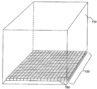
[046] FTG. l illustrates an exemplary arrangement of silicon seeds on the
bottom
surface of a crucible, according to an embodiment of the present invention;
[047] FIG. 2 illustrates another exemplary arrangement of silicon seeds on the
bottom and side surfaces of a crucible, according to an embodiment of the
present invention;
[048] FIG. 3A-3C illustrate an example of tiling for casting geometrically
ordered
multi-crystalline silicon in a crucible, according to an embodiment of the
present invention;
[049] FIG. 4 illustrates another example of tiling for casting geometrically
ordered
multi-crystalline silicon in a crucible, according to an embodiment of the
present invention;
[050] FIG. 5 illustrates an example of a close-packed array of hexagon seed
tiles,
according to an embodiment of the present invention;
[051] FIG. 6 illustrates an exemplary array of polygonal shapes having
rhomboid or
triangular interstices, according to an embodiment of the present invention
[052] FIG. 7 illustrates an cxcmplary method, according to an cmbodimcnt of
the
present invention; and
12
CA 02636031 2008-07-02
WO 2007/084934 PCT/US2007/060661
[053] FTGS. 8A-8G and 9 illustrate exemplary casting processes for
monocrystalline
or geometrically ordered multi-crystalline silicon, according to embodiments
of the present
invention.
DESCRIPTION OF THE EMBODIMENTS
[054] Reference will now be made in detail to embodiments of the present
invention,
examples of which are illustrated in the accompanying drawings. Wherever
possible, the
same or similar reference numbers will be used throughout the drawings to
refer to the same
or like parts.
[055] In embodiments consistent with the invention, the crystallization of
molten
silicon is conducted by casting processes using one or more seed crystals. As
disclosed
herein, such casting processes may be implemented so that the size, shape, and
orientation of
crystal grains in the cast body of crystallized silicon is controlled. As used
herein, the term
"cast" means that the silicon is formcd by cooling moltcn silicon in a mold or
vessel used to
hold the molten silicon. Since a liquid., such as molten silicon, will take
the shape of the
container in which it is placed, it is also contemplated herein that the
cooling of molten
silicon may also be accomplislied while confining the molten silicon by any
means, and not
just in a mold or vessel. By way of example, the silicon can be formed by
solidification in a
crucible, where solidification is initiated from at least one wall of the
crucible, and not
through a cooled foreign object introduced into the melt. The crucible may
have any suitable
shape, such as a cup, a cylinder, or a box. Thus, the process of molten
silicon crystallization
according to this invention is not controlled by "pulling" a boule or ribbon.
Further,
consistent with an embodiment of the present invention, the mold, vessel, or
crucible includes
at least one "hot side wall" surface in contact with the molten silicon. As
used herein, the
term "hot side wall" refers to a surface that is isothermal with or hotter
than the molten
silicon that it contacts. Preferably, a hot side wall surface remains fixed
during processing of
the silicon.
[056] Consistent with embodiments of the invention, the crystallized silicon
can be
either continuous monocrystalline, near-mono crystalline silicon, or
continuous geometric
multi-crystalline having controlled grain orientations. As used herein, the
term "continuous
monocrystallinc silicon" refers to single crystal silicon, where the body of
silicon is onc
homogeneous body of monocrystalline silicon and, not smaller pieces of silicon
joined
together to form a larger piece of silicon. Further, as used herein, the term
"continuous
geometric multi-crystalline silicon" refers to geometric multi-crystalline
silicon where the
13
CA 02636031 2008-07-02
WO 2007/084934 PCT/US2007/060661
body of silicon is one homogeneous body of geometric multi-crystalline silicon
and not
smaller pieces of silicon joined together to form a larger piece of silicon.
[057] Consistent with embodiments of the present invention, the
crystallization can
be accomplished by positioning a desired collection of crystalline silicon
"seeds" in, for
example, the bottom of a vessel, such as a quartz crucible that can hold
molten silicon. As
used herein, the term "seed" refers to a preferably geometrically shaped piece
of silicon with
a desired crystal structure, preferably wherein at least one cross-section has
a geometric,
preferably polygonal, shape, and preferably having a side that conforms to a
surface of a
vessel in which it may be placed. Such a sccd can be cithcr a monocrystalline
piccc of silicon
or a piece of geometrically ordered multi-crystalline silicon, for example, a
slab or horizontal
section cut or otherwise obtained from an ingot of monocrystalline silicon.
Consistent with
the present invention, a seed may have a top surface that is parallel to its
bottom surface,
although this does not have to be the case. For example, a seed can be a piece
of silicon,
varying in size from about 2 mm to about 3000 mm across. For example, a seed.
can be about
10 mm to about 300 mm across. The piece of silicon may have a thickness of
about 1 mm to
about 1000 mm, preferably about 5 mm to about 50 mm. A suitable size and shape
of the
seed may be selected for convenience and tiling. Tiling, which will be
described in more
detail below, is where silicon seed crystals are arranged in a predetermined
geometric
orientation or pattern across, for example, the bottom or one or more of the
sides and the
bottom surfaces of a crucible. It is preferable that the seed or seeds cover
the entire crucible
surface next to which they are located, so that when moving the seeded crystal
growth
solidification front away from the seeds, the full size of the crucible cross-
section can be
maintained as a consistent geometric crystal.
[058] The molten silicon is then allowed to cool and crystallize in the
presence of
the seeds, preferably in a manner such that the cooling of the molten silicon
is conducted so
that the crystallization of the molten silicon starts at or bclow the level of
the original top of
the solid seeds and proceeds away, preferably upwards away, from the seeds.
The solid-
liquid interface at an edge of the molten silicon will preferably initially
conform to a cooling
surface of the vessel, such as a surface in a crucible, in which it is being
cast. According to
embodiments of the invention, the liquid-solid interface between the molten
silicon and the
crystallized. silicon can be maintained substantially flat throughou.t part,
for example, the
initial part of the solidification stage, or all of the casting process. In an
embodiment of the
invention, the solid-liquid interface at each of the edges of the molten
silicon is controlled
during the cooling so as to move in a direction that increases a distance
between the molten
14
CA 02636031 2008-07-02
WO 2007/084934 PCT/US2007/060661
silicon and the cooled surface of the crucible while preferably maintaining a
substantially flat
solid-liquid interface.
[059] Therefore, consistent with the present invention, the solidification
front may
parallel the shape of a cooled surface of the vessel. For example, with a flat-
bottomed
crucible, the solidification front may remain substantially flat, with the
solid-liquid interface
having a controlled profile. The solid-liquid interface can be controlled so
that its radius of
curvature decreases as one moves from the edge to the center. Alternatively,
the solid-liquid
interface can be controlled to maintain an average radius of curvature of at
least half the
width of thc vcssel. Morcover, the solid-liquid interface can be controlled to
maintain an
average radius of curvature of at least twice the wid.th of the vessel. The
solid can have a
slightly convex interface with a radius of curvature at least about four times
the width of the
vessel. For example, the solid-liquid interface can have a radius of curvature
generally
greater than 2 m in a 0.7 m square crucible, more than twice the horizontal
dimension of the
crucible, and preferably about 8x to about 16x a horizontal dimension of the
crucible.
[060] According to embodiments of the present invention, a solid body of
monocrystalline silicon, or near-monocrystalline silicon, preferably cast,
preferably having at
least two dimensions each being at least about 20 cm, for example, at least
about 20 cm on a
side, and a third dimension at least about 10 cm, can be formed. Preferably, a
solid body of
monocrystalline silicon, or near-monocrystalline silicon, preferably cast,
having at least two
dimensions each being at least about 30 cm, for example, at least about 30 cm
on a side, and a
third dimension at least about 10 cm, can be formed. More preferably, a solid
body of
monocrystalline silicon, or near-monocrystalline silicon, preferably cast,
having at least two
dimensions each being at least about 35 cm, for example, at least about 35 cm
on a side, and a
third dimension at least about 10 cm, can be formed. Still more preferably, a
solid body of
monocrystalline silicon, or near-monocrystalline silicon, preferably cast,
having at least two
dimcnsions each being at least about 40 cm, for example, at least about 40 cm
on a side, and a
third dimension at least about 20 cm, can be formed. Still more preferably, a
solid body of
monocrystalline silicon, or near-monocrystalline silicon, preferably cast,
having at least two
dimensions each being at least about 50 cm, for example, at least about 50 cm
on a side, and a
third dimension at least about 20 cm, can be formed. Still more preferably, a
solid body of
monocrystalline silicon, or near-monocrystalline silicon, preferably cast,
having at least two
dimensions each being at least about 60 cm, for example, at least about 60 cm
on a side, and a
third dimension at least about 20 cm, can be formed. Still more preferably, a
solid body of
monocrystalline silicon, or near-monocrystalline silicon, preferably cast,
having at least two
CA 02636031 2008-07-02
WO 2007/084934 PCT/US2007/060661
dimensions each being at least about 70 cm, for example, at least about 70 cm
on a side, and a
third dimension at least about 20 cm, can be formed. According to embodiments
of the
present invention, a body of continuous monocrystalline silicon, or near-
monocrystalline
silicon, being free, or substantially free, of radially-distributed defects
and/or impurities,
preferably having at least two dimensions each being at least about 20 cm, and
a third
dimension at least about 10 cm, can be formed. Preferably, a body of
continuous
monocrystalline silicon, or near-monocrystalline silicon, being free, or
substantially free, of
radially-distributed defects and/or impurities, having at least two dimensions
each being at
least about 30 cm, and a third dimcnsion at least about 10 cm, can be formed.
More
preferably, a body of continuous monocrystalline silicon, or near-
monocrystalline silicon,
being free, or substantially free, of radially-distributed defects and/or
impurities, having at
least two dimensions each being at least about 35 cm, and a third dimension at
least about 10
cm, can be formed. Still more preferably, a body of continuous monocrystalline
silicon, or
near-monocrystalline silicon, being free, or substantially free, of rad.ially-
distribu.ted, defects
and/or impurities, having at least two dimensions each being at least about 40
cm, and a third
dimension at least about 20 cm, can be formed. Still more preferably, a body
of continuous
monocrystalline silicon, or near-monocrystalline silicon, being free, or
substantially free, of
radially-distributed defects and/or impurities, having at least two dimensions
each being at
least about 50 cm, and a third dimension at least about 20 cm, can be formed.
Still more
preferably, a body of continuous monocrystalline silicon, or near-
monocrystalline silicon,
being free, or substantially free, of radially-distributed defects and/or
impurities, having at
least two dimensions each being at least about 60 em, and a third dimension at
least about 20
cm, can be formed. Still more preferably, a body of continuous monocrystalline
silicon, or
near-monocrystalline silicon, being free, or substantially free, of radially-
distributed defects
and/or impurities, having at least two dimensions each being at least about 70
cm, and a third
dimension at least about 20 cm, can bc formed.
[0611 An upper limit of horizontal size of an ingot of cast silicon made
according to
embodiments of the invention is only determined by casting and crucible making
technology,
and not by the invented method itself. Ingots having a cross-sectional area of
at least 1 ma
and up to 4-8 m2 can be manufactured according to this invention. Similarly,
an upper limit
of the height of the ingot may be related to longer cycle times, and not the
fundamentals of
the casting process. Ingot heights of up to about 50 cm to about 80 cm are
possible. Thus,
consistent with the invention, a body of continuous monocrystalline silicon,
or near-
monocrystalline silicon, can be successfully grown to about 66 cm x 66 cm in
cross section,
16
CA 02636031 2008-07-02
WO 2007/084934 PCT/US2007/060661
with a rectangular solid piece of continuous monocrystalline silicon being at
least 33,750 cm3
in volume. Further, consistent with the present invention, a solid body of
cast continuous
monocrystalline silicon, or near-monocrystalline silicon, can be formed
preferably having at
least two dimensions each being as large as the interior dimensions of a
casting vessel and the
third dimension being the same height as the ingot. For example, if the cast
body of
monocrystalline silicon is a cube-shaped or a rectangular-shaped solid, these
dimensions
above would refer to the length, width, and height of such bodies.
[062] Similarly, a solid body of cast geometric multi-crystalline silicon,
preferably
having at lcast two dimcnsions each being at least about 10 cm, and a third
dimension at lcast
about 5 cm, can be formed.. Preferably, a solid body of cast geometric multi-
crystalline
silicon, having at least two dimensions each being at least about 20 cm, and a
third dimension
at least about 5 cm, can be forrned. More preferably, a solid body of cast
geometric multi-
crystalline silicon, having at least two dimensions each being at least about
30 cm, and a third
dimension at least about 5 cm, can be formed.. Still more preferably, a solid.
body of cast
geometric multi-crystalline silicon, having at least two dimensions each being
at least about
35 cm, and a third dimension at least about 5 cm, can be formed. Still more
preferably, a
solid body of cast geometric multi-crystalline silicon, having at least two
dimensions each
being at least about 40 cm, and a third dimension at least about 5 cm, can be
formed. Still
more preferably, a solid body of cast geometric multi-crystalline silicon,
having at least two
dimensions each being at least about 50 cm, and a third dimension at least
about 5 cm, can be
formed. Still more preferably, a solid body of cast geometric multi-
crystalline silicon, having
at least two dimensions each being at least about 60 cm, and a third dimension
at least about
5 cm, can be formed. Still more preferably, a solid body of cast geometric
multi-crystalline
silicon, having at least two dimensions each being at least about 70 cm, and a
third dimension
at least about 5 cm, can be formed. Thus, consistent with the invention, a
body of continuous
geometric multi-crystalline silicon can be successfully grown to about 66 cm x
66 cm in cross
section, with a rectangular solid piece of continuous geometric multi-
crystalline silicon being
at least 33,750 cm3 in volume. Further, consistent with the present invention,
a solid body of
cast geometric multi-crystalline silicon can be formed preferably having at
least two
dimensions each being as large as the interior dimensions of a casting vessel.
For example, if
the cast body of geometric multi-crystalline silicon is a cube-shaped or a
rectangular-shaped.
solid, these dimensions above would refer to the length, width, and height of
such bodies.
[063] By conducting the crystallization of the molten silicon in a manner
consistent
with embodiments of the invention, cast silicon having specific, rather than
random, grain
17
CA 02636031 2008-07-02
WO 2007/084934 PCT/US2007/060661
boundaries and specific grain sizes can be rnade. Additionally, by aligning
the seed(s) in a
manner such that all seeds are oriented the same relative direction to each
other, for example
the (100) pole direction being perpendicular to a bottom of the crucible and
the (110) pole
direction parallel to one of the sides of a rectangular or square cross-
section crucible, large
bodies of cast silicon can be obtained that are, or are nearly,
monocrystalline silicon in which
the pole direction of such cast silicon is the same as that of the seed(s).
Similarly, other pole
directions may be perpendicular to the bottom of the crucible. Moreover,
consistent with an
embodiment of the invention, the seed(s) may be arranged so that any common
pole direction
is perpendicular to a bottom of the cruciblc.
[064] When monocrystalline silicon is made by the conventional method of
pulling a
cylindrically shaped boule from a pool of molten silicon, e.g., according to
the CZ or FZ
methods, the monocrystalline silicon obtained contains radially distributed
impurities and
defects, such as swirl defects (forrned from intrinsic defects such as
vacancies and self-
interstitial atoms) and OSF ring defects. Swirl defects are interstitial
silicon atoms or
vacancies, either in singular or clustered form. Such swirl defects can be
detected by x-ray
topography and appear as "swirls" in the silicon. They can also be detected
after preferential
acid etching of the silicon for defect delineation.
[065] According to the conventional CZ or FZ methods, the distribution of
oxygen
atoms within the silicon and the defects in the silicon caused by such oxygen
atoms are
radially situated. This means that they tend to be arranged in rings, spirals
or striations that
are symmetric about a central axis. OSF ring defects are a particular example
of this, where
nanometer-scale oxygen precipitates nucleate stacking faults in a cylindrical
band within a
pulled monocrystalline ingot or boule of silicon, resulting in circular defect
bands on wafers
made from such silicon. Such bands can be observed in a sample of silicon
after preferential
acid etching.
[066] Both swirl defects and OSF ring dcfccts occur in the boulcs of
monocrystalline
silicon by pulling a cylindrically shaped boule from a pool of molten silicon,
e.g., according
to the conventional CZ or FZ methods, due to the rotational symmetry of the
pulling process,
the axial thermal gradients, and the rotation inherent in the process. In
contrast, silicon can
be made by casting processes according to embodiments of the invention that
does not exhibit
such swirl defects and OSF ring defects. This is because the incorporation of
defects during
the casting process can be essentially distributed randomly at a growth
interface not
influenced by rotation, in a body of silicon that does not possess cylindrical
symmetry, and in
18
CA 02636031 2008-07-02
WO 2007/084934 PCT/US2007/060661
a process where the isotherms are essentially flat across the ingot throughout
the
solidification and the cool-down processes.
[067] Concerning the concentrations of light element impurities in silicon
grown by
different methods, the following levels, shown in TABLE 1, are widely
considered
characteristic.
[068] TABLE 1
Concentrations (atoms/cm )
Oxygen Carbon Nitrogen
F1oat Zone < 1x10¹⁶ < 1x10¹⁶ < 1x10¹⁴
Czochralski 2x10¹⁷ - 1x10¹⁸ < 1x10¹⁶ < 5x10¹⁴
Cast 2-3x10¹⁷ 2x10¹⁶ - 5x10" > 1x10¹⁵
[069] Parts of CZ ingots can be produced with as low as 5x10¹⁷ atoms/cm3 of
oxygen, but not lower. Carbon and nitrogen concentrations can be increased in
FZ and CZ
ingots by intentional doping, but doping does not exceed the solid solubility
limit in these
techniques (as it does in cast material), and doped ingots have not been made
in sizes larger
than 20 cm diameter. By contrast, cast ingots are typically supersaturated
with carbon and
nitrogen due to release coatings and the design of the furnace hot zone. As a
consequence,
precipitated nitrides and carbides are ubiquitous due to liquid phase
nucleation and growth.
Furthcrmorc, cast single crystal ingots havc bccn manufactured, according to
cmbodimcnts of
the invention, with the above-reported impurity levels and with sizes as large
as 50x50x20
cm3 and 60x60x5 cm3. These dimensions are exemplary only, and are not
considered upper
limits for the casting processes of the invention.
[070] For example, regarding impurity levels, a dissolved carbon concentration
of
about 1-5x10¹⁷ atoms/cm3 (notation for about 1x10¹⁷ atoms/cm3 to about 5x10¹⁷
atorns/cm)
,
a dissolved oxygen concentration of about 2-3x10¹⁷ atoms/cm3, and a dissolved
nitrogen
concentration of about 1-5x10¹⁵ atoms/cm3 are preferred in the silicon cast
according to this
19
CA 02636031 2008-07-02
WO 2007/084934 PCT/US2007/060661
invention. According to embodiments of the present invention, a solid body of
monocrystalline silicon, or near-monoccrystalline silicon, preferably cast,
preferably having at
least two dimensions each being at least about 20 cm, for example, at least
about 20 cm on a
side, and a third dimension at least about 10 cm, can be formed, having a
dissolved carbon
concentration of about 1-5x10¹⁷ atoms/cm3, a dissolved oxygen concentration of
about 2-
3x10¹⁷ atoms/cm3, and a dissolved nitrogen concentration of about 1-5x10¹⁵
atoms/cm3.
Preferably, a solid body of monocrystalline silicon, or near-monocrystalline
silicon,
preferably cast, having at least two dimensions each being at least about 30
cm, for example,
at least about 30 cm on a sidc, and a third dimension at least about 10 cm,
can be formcd,
having a d.issolved. carbon concentration of about 1-5x10¹⁷ atoms/cm3, a
dissolved oxygen
concentration of about 2-3x10¹⁷ atoms/cm3, and a dissolved nitrogen
concentration of about
1-5x10¹⁵ atoms/cm3. More preferably, a solid body of monocrystalline silicon,
or near-
monocrystalline silicon, preferably cast, having at least two dimensions each
being at least
about 35 cm, for example, at least about 35 cm on a side, and. a third.
dimension at least about
10 cm, can be formed, having a dissolved carbon concentration of about 1-
5x10¹⁷ atoms/cm3,
a dissolved oxygen concentration of about 2-3x10¹⁷ atoms/cm~, and a dissolved
nitrogen
concentration of about 1-5x10¹⁵ atoms/cm3. Still more preferably, a solid body
of
monocrystalline silicon, or near-monocrystalline silicon, preferably cast,
having at least two
dimensioans each being at least about 40 cm, for example, at least about 40 cm
on a side, and a
third dimension at least about 20 cm, can be formed, having a dissolved carbon
concentration
of about 1-5x10¹⁷ atoms/cm3, a dissolved oxygen concentration of about 2-
3x10¹⁷ atoms/cm3,
and a dissolved nitrogen concentration of about 1-5x10¹⁵ atoms/cm3. Still more
preferably, a
solid body of monocrystalline silicon, or near-monocrystalline silicon,
preferably cast, having
at least two dimensions each being at least about 50 cm, for example, at least
about 50 cm on
a side, and a third dimension at least about 20 cm, can be formed, having a
dissolved carbon
conccntration of about 1-5x10¹⁷ atoms/cm3, a dissolved oxygen concentration of
about 2-
3x10¹⁷ atoms/cm3, and a dissolved nitrogen concentration of about 1-5x10¹⁵
atoms/cm3. Still
more preferably, a solid body of monocrystalline silicon, or near-
monocrystalline silicon,
preferably cast, having at least two dimensions each being at least about 60
cm, for example,
at least about 60 cm on a side, and a third dimension at least about 20 Cm,
can be formed,
having a dissolved. carbon concentration of about 1-5x10¹⁷ atoms/cm3, a
dissolved. oxygen
concentration of about 2-3x10¹⁷ atoms/crn3, and a dissolved nitrogen
concentration of about
1-5x10¹⁵ atoms/cm;. Still more preferably, a solid body of monocrystalline
silicon, or near-
monocrystalline silicon, preferably cast, having at least two dimensions each
being at least
CA 02636031 2008-07-02
WO 2007/084934 PCT/US2007/060661
about 70 cm, for example, at least about 70 cm on a side, and a third
dimension at least about
20 cm, can be formed, having a dissolved carbon concentration of about 1-5x
1017 atoms/cm3,
a dissolved oxygen concentration of about 2-3x10" atoms/cm~, and a dissolved
nitrogen
concentration of about 1-5x10¹⁵ atoms/cm3.
[071] According to embodiments of the present invention, a body of continuous
monocrystalline silicon, or near-monocrystalline silicon, being free, or
substantially free, of
radially-distributed defects and/or impurities, preferably having at least two
dimensions each
being at least about 20 cm, and a third dimension at least about 10 cm, can be
formed, having
a dissolved carbon conccntration of about 1-5xl017 atoms/cm3, a dissolved
oxygen
concentration of about 2-3x10¹⁷ atoms/crri , and. a dissolved, nitrogen
concentration of about
1-5x10¹⁵ atoms/cm3. Preferably, a body of continuous monocrystalline silicon,
or near-
monocrystalline silicon, being free, or substantially free, of radially-
distributed defects and/or
impurities, having at least two dimensions each being at least about 30 cm,
and a third
dimension at least about 10 cm, can be formed., having a d.issolved. carbon
concentration of
about 1-5x10¹⁷ atoms/cm3, a dissolved oxygen concentration of about 2-3x10¹⁷
atoms/cm3,
and a dissolved nitrogen concentration of about 1-5x10¹⁵ atoms/em;. More
preferably, a
body of continuous monocrystalline silicon, or near-monocrystalline silicon,
being free, or
substantially free, of radial ly-distributed defects and/or impurities, having
at least two
dimensions each being at least about 35 cm, and a third dimension at least
about 10 cm, can
be formed, having a dissolved carbon concentration of about 1-5x10" atoms/cm?,
a dissolved
oxygen concentration of about 2-3x10¹⁷ atoms/cm3, and a dissolved nitrogen
concentration of
about 1-5x10¹⁵ atoms/cm3. Still more preferably, a body of continuous
monocrystalline
silicon, or near-monocrystalline silicon, being free, or substantially free,
of radially-
distributed defects and/or impurities, having at least two dimensions each
being at least about
40 cm, and a third dimension at least about 20 cm, can be formed, having a
dissolved carbon
concentration of about 1-5x10¹⁷ atoms/crn3, a dissolved oxygen concentration
of about 2-
3x10¹⁷ atoms/cm3, and a dissolved nitrogen concentration of about 1-5x10¹⁵
atoms/cm3. Still
more preferably, a body of continuous monocrystalline silicon, or near-
rnonocrystalline
silicon, being free, or substantially free, of radially-distributed defects
and/or impurities,
having at least two dimensions each being at least about 50 cm, and a third
dimension at least
about 20 cm, can be formed, having a dissolved carbon concentration of about 1-
5x10¹⁷
atoms/cm3, a dissolved oxygen concentration of about 2-3x10¹⁷ atoms/cm3, and a
dissolved
nitrogen concentration of about 1-5x10¹⁵ atoms/cm3. Still more preferably, a
body of
continuous monocrystalline silicon, or near-monocrystalline silicon, being
free, or
21
CA 02636031 2008-07-02
WO 2007/084934 PCT/US2007/060661
substantially free, ofradially-distributed defects and/or impurities, having
at least two
dimensions each being at least about 60 cm, and a third dimension at least
about 20 cm, can
be formed, having a dissolved carbon concentration of about 1-5x10" atoms/cm~,
a dissolved
oxygen concentration of about 2-3x10¹⁷ atoms/cm3, and a dissolved nitrogen
concentration of
about 1-5x10¹⁵ atoms/cm3. Still more preferably, a body of continuous
monocrystalline
silicon, or near-monocrystalline silicon, being free, or substantially free,
of radially-
distributed defects and/or impurities, having at least two dimensions each
being at least about
70 cm, and a third dimension at least about 20 cm, can be formed, having a
dissolved carbon
conccntration of about 1-5x10¹⁷ atoms/cm3, a dissolvcd oxygen concentration of
about 2-
3x10¹⁷ atoms/cm3, and a dissolved nitrogen concentration of about 1-5x10¹⁵
atoms/cm3.
[072] An upper limit of horizontal size of an ingot of cast silicon made
according to
embodiments of the invention, and having the above-referenced impurity
concentrations, is
only determined by casting and crucible making technology, and not by the
invented method
itself. Thus, consistent with the present invention, a solid. body of cast
continuous
monocrystalline silicon, or near-monocrystalline silicon, having the above-
referenced
impurity concentrations, can be formed preferably having at least two
dimensions each being
as large as the interior dimensions of a casting vessel and the tliird
dimension being the same
height as the ingot. For example, if the cast body ofmonocrystalline silicon
is a cube-shaped
or a rectangular-shaped solid, these dimensions above would refer to the
length, width, and
height of such bodies.
[073] The seed(s) used for casting processes, consistent with embodiments of
the
invention, can be of any desired size and shape, but are suitably
geometrically shaped pieces
of monocrystalline silicon, near-monocrystalline silicon, or geometrically
ordered multi-
crystalline silicon, such as square, rectangular, hexagonal, rhomboid or
octagonal shaped
pieces of silicon. They can be shaped conducive to tiling, so they can be
placed or "tiled"
cdgc-to-cdgc and conformcd to the bottom of a cruciblc in a dcsircd pattcrn.
Also consistcnt
with embodiments of the invention, seeds can be placed on one or more,
including all, sides
of the crucible. Such seeds can be obtained, for example, by sawing a source
of crystalline
silicon, such as a boule of monocrystalline silicon, into pieces having the
desired shapes. The
seeds can also be formed by cutting them from a sample of either continuous
monocrystalline, near-monocrystalline silicon, or continuous geometric multi-
crystalline
silicon made by a process according to embodiments of the invention, such that
seed(s) for
use in subsequent casting processes can be made from an initial casting
process. Thus, for
example, a slab of either continuous monocrystalline or near-monocrystalline
silicon cut or
22
CA 02636031 2008-07-02
WO 2007/084934 PCT/US2007/060661
otherwise obtained from an ingot of continuous monocrystalline or near-
monocrystalline
silicon can function as a template for a subsequent casting of continuous
monocrystalline or
near-monocrystalline silicon. Such a seed crystal can be the size and shape,
or substantially
the size and shape, of a side, such as the bottom, of a crucible or other
vessel in which the
seed is placed. For the purposes of monocrystalline casting, it is preferable
to have as few
seeds as possible to cover the crucible bottom in order to avoid the
incorporation of defects.
Thus, the seed or seeds can be the size and shape, or substantially the size
and shape, of one
or more sides, such as the bottom, of a crucible or other vessel in which the
seed or seeds is
placed to perform the casting method in accordance with this invcntion.
[074] Processes and apparatuses for preparing silicon in accordance with
certain
embodiments of the invention will now be described. However, it is to be
understood that
these are not the only ways to form silicon consistent with the principles of
the invention.
[075] Referring to FIG. 1, seeds 100 are placed at the bottom of a bottomed
and
walled cru.cible 110, such as a quartz crucible, in a way such that either
they closely abut in
the same orientation so as to form a large, continuously oriented slab 120.
Alternatively, they
closely abut in pre-selected rnisorientations so as to produce specific grain
boundaries with
deliberately chosen grain sizes in the resulting silicon that is produced.
That is, for casting of
geometric multi-crystalline silicon, the cross-sectional grain size and,
preferably, cross-
sectional shape of the resulting crystallized geometric multi-crystalline
silicon will be equal
to or will approximate that of the seeds and the height of the grain can be a
long as the
dimension of the silicon that is perpendicular to the cross-section. If a
geometric multi-
crystalline seed crystal, for example, a slab of geometric multi-crystalline
silicon cut or
otherwise obtained from an ingot of geometric multi-crystalline silicon, is
used a seed crystal
or seed crystals for casting geometric multi-crystalline silicon, the cross-
sectional grain size
and, preferably, cross-sectional shape of the grains of the resulting
geometric multi-
crystalline silicon will approximate the grains in the geometric multi-
crystallinc seed or
seeds. Thus, a slab of geometric rnulti-crystalline silicon cut or otherwise
obtained from an
ingot of geometric multi-crystalline silicon can be a "geometric multi-
crystalline silicon seed
crystal" (also referred to as a "geometrically ordered multi-crystalline
silicon seed crystal"),
and can function as a template for a subsequent casting of geometric multi-
crystalline silicon.
Such a seed. crystal can be the size and. shape, or substantially the size
and. shape, of a side,
such as the bottom, of a crucible or other vessel in which the seed is placed.
When such a
seed crystal is used in the method of this invention, the resulting geometric
multi-crystalline
23
CA 02636031 2008-07-02
WO 2007/084934 PCT/US2007/060661
silicon will preferably have crystal grains that have the same or
substantially the same cross-
sectional size and shape as the grains in the seed.
[076] Preferably, seeds 100 are tiled and placed so as to substantially cover
the
entirety of the bottom of crucible 110. It is also preferable that crucible
110 has a release
coating such as one made from silica, silicon nitride, or a liquid
encapsulant, to aid in the
removal of crystallized silicon from crucible 110. Further, the seeds may
comprise a slab or
slabs of monocrystalline silicon of a desired crystal orientation, about 3 mm
to about 100 mm
thick. While a specific number and size of seeds 100 is shown in FIG. 1, it
will be readily
apparcnt to one of ordinary skill in the art that both the number and size of
the sccds can bc
increased or decreased, depending on the application.
[077] Referring to FIG. 2, seeds 100 can also be placed on one or more side
walls
130, 140 of crucible 110. Seeds 100 can be placed on all four walls of
crucible 110, although
for illustration purposes only, seeds 100 are shown only on walls 130, 140.
Preferably, the
seeds 100 that are placed on any of the four walls of crucible 110 are
columnar to facilitate
crystal growth. Preferably, each of the columnar seeds placed on any of the
four walls of
crucible 110 will have the same grain orientation as the seed placed
immediately below it on
the bottom surface of crucible 110. In the case of geometric multi-crystalline
silicon growth,
placing the columnar seeds in this manner will facilitate the growth of
geometric multi-
crystalline silicon grains as large as the height of the crucible 110.
[078] Still referring to FIG. 2, advantages of this arrangement of seeds 110
are a
quicker, more simple, self-propagating process for casting silicon with higher
crystallinity and
higher growth rates. For example, silicon may be melted in a silicon `cup',
consisting of many
seeds that are stacked together to form a cavity, e.g:, a bottom and four
walls, inside crucible
110. Alternatively, molten silicon may be poured in a silicon `cup',
consisting of many seeds
that are stacked together to form a cavity, e.g., a bottom and four walls,
inside crucible 110. In
an altcrnativc cxamplc, the receiving `cup' is first brought up to the melting
tcmpcraturc of
silicon, but maintained in solid state, and then the molten silicon is poured
in and allowed to
come to thermal equilibrium. Then, in either example above, crucible 110 is
cooled, whereby
heat is removed from the bottom and sides of crucible 110 by, for example, a
solid heat sink
material (not shown) which radiates heat to the ambient, while heat is still
applied to the open
top of crucible 110. In this way, the resulting cast ingot of silicon may be
either monocrystalline
or geometric multi-crystalline (depending on the type of seeds 100 used and
their orientation),
and the crystallization proceeds faster than known multi-crystalline casting
processes. To repeat
this process, a portion of the sides and bottom of the crystallized silicon
ingot are removed,
24
CA 02636031 2008-07-02
WO 2007/084934 PCT/US2007/060661
using known techniques, and can be reused in a subsequent casting process.
Preferably, a
plurality of seed crystals, e.g., seeds 100, are arranged so that a common
pole direction
among seeds 100 is perpendicular to each of the bottom and a side of crucible
110, so that no
grain boundaries are formed between the bottom and a side of crucible 110.
[079] FIGS. 3A-3C illustrate an example of tiling for casting geometric multi-
crystalline silicon in crucible 110. Crystal grain engineering can be achieved
by careful seed
creation, orientation, placement, and crystal growth. FIGS. 3A and 3B, for
example, show two
monocrystalline silicon slabs 155, 165, on which different (110) directions
are indicated.
Both slabs have a common (100) direction perpendicular to their surfaces. Each
slab of
monocrystalline silicon 155, 165, is then cut to form many pieces of silicon,
which become
seeds 150, 160. The surface types can be uniform, e.g., (100), for texturing
reasons, or chosen at
will. The shape and size of grains may be selected based on the cutting of the
tiles from slabs of
monocrystalline silicon 155 and 165, as shown in FIG. 3B. The relative
orientation angles
between neighboring tiles of pieces 150, 160, d.etermin.es the grain boundary
type (e.g., high
angle, low angle or twin) in the resulting cast geometric multi-crystalline
silicon. In FIG. 3A,
for example, two grain orientations of the (100) pole direction are shown.
[080] The seeds shown in FIG. 3C are then comprised of tiled monocrystalline
silicon
pieces 150, 160 that have specifically selected orientation relationships with
their neighboring
tiles. Silicon pieces 150, 160 are then tiled in the bottom of crucible 110,
shown in FIG. 3C,
such that the two (110) directions are alternating, as shown by the arrows
drawn on pieces 150,
160. It is important to note that pieces 150, 160 are drawn as roughly square
blocks for
illustrative purposes only, and for the reasons discussed below, could be
other shapes.
[081] Although not shown in FIG. 3C, seeds may also be located on the sides of
crucible, as in FIG. 2. Silicon feedstock (not shown) may then be introduced
into crucible 110
over pieces 150, 160, and then melted. Alternatively, molten silicon may be
poured in crucible
110. In the altcrnativc example, cruciblc I 10 is first brought very closc to
or up to the mclting
temperature of silicon, and then the molten silicon is poured in. Consistent
with embodiments of
the invention, a thin layer of the seeds can be melted before solidification
begins.
[082] Then, in either example above, crucible 110 is cooled, whereby heat is
removed
from the bottom of crucible 110 (and sides only if seeds are tiled on the side
surfaces as well)
by, for example, a solid heat sink material which radiates heat to the
ambient, while heat is still
applied to the open top of crucible 110. Thus, melted silicon is introduced
while the seed is
maintained as a solid, and directional solidification of the melt causes the
upwards growth of the
columnar grains. In this way, the resulting cast ingot of geometric multi-
crystalline silicon will
CA 02636031 2008-07-02
WO 2007/084934 PCT/US2007/060661
mimic the grain orientations of tiled silicon seeds 150, 160. Once this
technique is properly
implemented, the resulting ingot can be cut into, for example, horizontal
slabs to act as seed
layers for other casting processes. The slab can have, for example, the size
and shape, or
substantially the size and shape, of a surface, such as a bottom, of a
crucible or other vessel used
for the casting. For example, only one such slab can be used for a casting
process.
[083] FIG. 4 illustrates a variation of the tiling shown in FIG. 3C. As an
example of
grain orientation for cast geometric multi-crystalline silicon, seed pieces
150, 160 are tiled
with a common pole direction (001) being perpendicular to the bottom of
crucible 110. In
FIG. 4, all variations of the (110) family of directions arc rcprescntcd in
the tiling of pieces
150, 160, as indicated by the directional arrows. Although not shown in this
particular figure,
seeds can also be on one or more sides of crucible 110.
[084] Thus, the orientation of seed crystals in a crucible used to form the
silicon may
be chosen such that specific grain boundaries are formed in cast geometric
multi-crystalline
silicon, and. where such grain boundaries enclose geometric shapes. In
contrast to
embodiments of the invention, known casting processes involve the casting of
multi-crystalline
grains in an uncontrolled fashion by directional solidification from a
completely melted mass of
silicon. The resulting grains have basically random orientation and size
distribution. The
random grain orientation makes it difficult to effectively texture the silicon
surface.
Furthermore, it has been shown that kinks in the grain boundaries, natural
products of the typical
growth techniques, tend to nucleate structural defects involving clusters or
lines of dislocations.
These dislocations, and the impurities that they tend to attract, cause fast
recombination of
electrical carriers and the degradation of perforrnance as a photovoltaic
material. Therefore,
consistent with an embodiment of the invention, careful planning and seeding
of a regular
grain boundary network for casting of either monocrystalline or geometric
multi-crystalline
silicon is accomplished such that the size, shape and orientation of grains is
explicitly chosen
to maximize minority carricr lifctimc and impurity gettering while rninimizing
structural
defects.
[085] Grain boundaries can be chosen to be flat planes in order to minimize
dislocation nucleation while maintaining their vertical direction during
growth. The grain
boundary types are chosen to maximize gettering of impurities and stress
relief. The grain
orientations (and. especially the surface orientation) are chosen to allow
texturing, improve
surface passivation and enhance grain strength. The size of the grains is
chosen to optimize
the balance between effective gettering distances and large absorption areas.
For example,
casting of geometric multi-crystalline silicon can be accomplished such that
the geometric
26
CA 02636031 2008-07-02
WO 2007/084934 PCT/US2007/060661
multi-crystalline silicon has an average minimum grain cross-section size of
at least about 0.5
cm to about 10 cm with a common pole direction being perpendicular to the
surface of the
cast geometric multi-crystalline silicon, as shown, for example, in FIGS. 3C
and 4. The
average crystal grain cross-section size can be about 0.5 cm to about 70 cm,
or larger. As
described above, the cross-section size is understood as the longest dimension
of the cross-
section of the grain that is perpendicular to the height or length of the
grain. The net result is
an overall increase in efficiency of the resulting photovoltaic material.
[086] Consistent with an embodiment of the invention, a geometric arrangement
of a
plurality of monocrystallinc silicon seed crystals can be placed on at least
one surface in a
crucible, e.g., a bottom surface of a crucible, wherein the geometric
arrangement includes
close-packed polygons. Alternatively, a geometric arrangement of a plurality
of
monocrystalline silicon seed crystals can be placed such that the geometric
arrangement
includes close-packed hexagons, or polygonal shapes having rhomboid or
triangular
interstices, as shown, for example, in FIGS. 5 and. 6. In yet another
alternative, instead of
using a plurality of monocrystalline seed crystals, a section or slab of
silicon cut or otherwise
obtained from an ingot produced in a prior casting of monocrystalline silicon
or near-
monocrystalline silicon can be used as a single seed crystal for casting
monocrystalline
silicon or near-monocrystalline silicon in accordance with this invention.
Such a single seed
crystal can be the same size and shape, or substantially the same size and
shape, as a surface
of the crucible or other vessel used to conduct the casting. More
specifically, FIG. 5
illustrates an example of a close-packed array of hexagons 170. In contrast,
FIG. 6 illustrates
an example of an array of polygonal shapes having rhomboid or triangular
interstices 180,
190. Both arrays are discussed in more detail below. Any of the arrangements
discussed
above are also applicable to an embodiment for casting either a solid body of
monocrystalline
silicon, a solid body of near-monocrystalline silicon, or a solid body of
geometric multi-
crystalline silicon, whcrc the secd crystals are so placed on both the bottom
and side surfaccs
of a crucible.
[087] The silicon crystal grains produced by casting a body of geometric multi-
crystalline silicon, consistent with embodiments of the invention, may be
grown in a
columnar manner. Further, such crystal grains may have a cross section that
is, or is close to,
the shape of the seed from which it is forxned.. When making silicon that has
such
specifically selected grain boundaries, preferably the grain boundary
junctions only have
three grain boundaries meeting at a corner. As shown in FIG. 5, hexagonal
arrangements of
seed crystals 170 are desirable for the tiling of seeds where the crystal
orientation is such that
27
CA 02636031 2008-07-02
WO 2007/084934 PCT/US2007/060661
the atoms in the horizontal plane have three-fold or six-fold symmetry, such
as (1 1 1) for
silicon. Thus, FIG. 5 illustrates a plan view of a portion of a collection of
hexagonal-shaped
seeds for arrangement in the bottom of a suitable crucible, such as that shown
in FIGS. 1 and
2. The arrows indicate the orientation of the (110) direction of the silicon
crystal in the seeds.
[088] Alternatively, for orientations with 4-fold syyinmetry, a different
geometric
configuration of the seeds can be used to maintain stable, symmetric grain
boundaries across
multiple grains while still meeting the three grain boundary corner rule. For
example, if 0 is
the misorientation between the (110) direction and the primary sides of an
octagon with a
(100) pole, and a is the apex angle of an interstitial rhombus, as shown in
FIG. 6, all crystal
grains will have a symmetric grain boundary with respect to the (110)
direction if a = 90 - 0.
In this example, all crystal grains have a (100) pole direction perpendicular
to the plane of the
paper on which FIG. 6 is depicted. Thus, FIG. 6 is a plan view of a portion of
a collection of
octagonal-shaped seeds along with rhombus-shaped seeds 180, 190 for
arrangement in the
bottom of a suitable crucible, such as that shown in FIGS. 1 and 2. The arrows
indicate the
orientation of the (110) direction of the silicon crystal in the seeds.
[089] FIG. 7 is a flowchart depicting an exemplary method of making silicon,
consistent with the present invention. Consistent with FIG. 7, method 700 may
begin by
selecting monocrystalline silicon seed crystals for monocrystalline or
geometric multi-
crystalline silicon growth, and arranging the monocrystalline silicon seed
crystals in a
crucible (step 705). Alternatively, a single slab cut or otherwise obtained
from an ingot of
monocrystalline silicon or geometrically ordered multi-crystalline silicon can
be used as a
single seed crystal. Next, silicon feedstock may be added to the crucible
(step 710). The
crucible is then heated from the top while the bottom of the crucible is
cooled from the
bottom (either passively or actively; see step 715). During melting, the melt
stage of the
silicon is monitored to track and control the position of the solid-liquid
interface (step 720).
The melt stage of the silicon is allowed to proceed until a portion of the
monocrystalline
silicon seed crystals are melted (step 725). Once a desired portion of the
monocrystalline
silicon seed crystals are melted, the melt stage is ended and the crystal
growth stage begins
(step 730). The crystal growth is allowed to continue unidirectionally and
vertically within
the crucible until thc silicon crystallization is complete (stcp 735). If thc
sccds arc arranged
for geometric multi-crystalline silicon growth, the crystallization of step
735 will produce a
geometric multi-crystalline silicon ingot with columnar grains (step 740).
Alternatively, if
the seeds are arranged for monocrystalline silicon growth, the crystallization
of step 735 will
28
CA 02636031 2008-07-02
WO 2007/084934 PCT/US2007/060661
produce a monocrystalline silicon ingot (step 745). Finally, the ingot
produced in either step
740 or 745 is removed for further processing (step 750).
[090] As shown in FIG. 8A, silicon feedstock 200 may be introduced to crucible
210
containing seeds 220 in, for example, one of two ways. In the first, crucible
210 is loaded to
full capacity with solid silicon feedstock 200, suitably in the form of
conveniently sized
chunks, and the loaded crucible 210 is placed in a casting station (not
shown).
[091] As shown in FIG. 8B, the thermal profile in crucible 210 is set up so
that the
top of the silicon charge in crucible 110 is heated to melting, while the
bottom is actively or
passively cooled to maintain the solid phase of seeds 220 at the bottom of
crucible 210, i.e.,
so that they do not float when feedstock 200 is melted.. A solid. heat sink
materia1230 is in
contact with a bottom of crucible 210 for radiating heat to water-cooled
walls. For example,
heat sink material 230 can be a solid block of graphite, and can preferably
have dimensions as
large or larger than the bottom of the crucible. Consistent with the
invention, for example, the
heat sink material can be 66 em by 66 cm by 20 cm, when used with a crucible
having a bottom
surface that is 66 cm by 66 cm. The side walls of crucible 210 are,
preferably, not cooled in
any way, provided that seeds 220 are located only on the bottom of crucible
210. If seeds
220 are located on the bottom and sides of crucible 210, then heat sink
material 230 would be
placed on both the bottom and sides of crucible 210 for maintaining the
desired thermal
profile.
[092] The melting phase of silicon feedstock 200 is closely monitored to track
the
position of the interface between the melted silicon and the seeds.
Preferably, melt 240
(shown in FIG. 8B) proceeds until all of the feedstock silicon 200 except for
seeds 220 is
completely melted, after which seeds 220 are partially melted. For example,
the heating can
be closely controlled such that the seeds 220 do not melt completely, by
maintaining a AT of
about 0.1 C/min or less, as measured on an outside surface of the crucible,
after reaching the
melting temperature of silicon elsewhere in the cruciblc. Prcfcrably, the
heating can be
closely controlled by maintaining a AT of about 0.05 C/min or less, as
measured on an
outside surface of the crucible, after reaching the melting temperature of
silicon elsewhere in
the crucible. For example, consistent with the invention, the AT can be
measured on an
outside surface of the crucible between the crucible and a large block of
graphite, and a dip-
rod. may be inserted into melt 240 to measure the depth of the melt, in order
to calculate the
portion of seeds 220 that have melted.
[093] As shown in FIG. 8C, portion 250 illustrates a melted portion of the
total
thickness of seeds 220, below the melt 240. After a portion 250 of seeds 220
are melted
29
CA 02636031 2008-07-02
WO 2007/084934 PCT/US2007/060661
below melt 240, the melt stage is then quickly ended and the crystal growth
stage is begun,
wherein the heating at the top of crucible 210 is decreased and/or the cooling
of the bottom at
heat sink material 230 is increased. As an example of this process, the chart
shown in FIG.
8D illustrates melting of a portion 250 of seeds 220 as a function of time. As
shown in FIG.
8D, a portion of the seeds having an initial thickness between 5 and. 6 cm are
gradually
melted until just under 2 cm of solid seed remains. For example, the heating
can be closely
controlled such that the seeds 220 do not melt completely, by maintaining a AT
of about 0.1
C/rnin or less, as measured on an outside surface of the crucible (e.g.,
through a
thcrmocouplc mounted in the cooling block), after reaching the melting
temperature of
silicon elsewhere in the crucible. Preferably, the heating can be closely
controlled by
maintaining a AT of about 0.05 C/min or less, as measured on an outside
surface of the
crucible, after reaching the melting temperature of silicon elsewhere in the
crucible. At this
point, the melt stage is then quickly ended and the crystal growth stage is
begun, which is
indicated. by the comparative rise in solid thickness measured, on the
ordinate of the chart.
[094] Then, as shown in FIG. 8E, seeded crystal growth continues
unidirectionally,
and vertically, within crucible 210 until the silicon crystallization is
complete. The casting
cycle finishes when the top-to-bottom thermal gradient within crucible 210 is
evened out.
Then, the entire ingot 260 is slowly cooled down to room temperature. For
casting of
geometric multi-crystalline silicon, as shown in FIG. 8E, this seeded
unidirectional growth
produces columnar shaped grains 270 having, generally, a horizontal cross
section that is the
shape of the individual seed 220 over which it is formed. In this manner, the
grain
boundaries of the cast geometric multi-crystalline silicon can be pre-
selected. Any of the
previously discussed seeding patterns / tiling are applicable to this casting
process.
[095] Alternatively, for casting of monocrystalline silicon, the arrangement
of seeds
220 can be made to have no grain boundaries at all, resulting in cast
monocrystalline silicon.
As shown in FIG. 8F, portion 250 illustratcs a melted portion of the total
thickness of seeds
220, below the melt 240. After a portion 250 of seeds 220 are melted below
melt 240, the
melt stage is then quickly ended and the crystal growth stage is begun,
wherein the heating at
the top of crucible 210 is decreased and/or the cooling of the bottom at heat
sink material 230
is increased. Then, as shown in FIG. 8G, seeded crystal growth continues
unidirectionally,
and. vertically, within crucible 210 until the silicon crystallization is
complete. A preferably
substantially flat solid-liquid interface 285 propagates upward and away from
a bottom
surface of crucible 210. The casting cycle finishes after the completion of
crystal growth,
when the top-to-bottom thermal gradient within crucible 210 is evened out.
Then, the entire
CA 02636031 2008-07-02
WO 2007/084934 PCT/US2007/060661
ingot 280 is slowly cooled down to room temperature. For casting of
monocrystalline silicon,
as shown in FIG. 8G, this seeded unidirectional growth produces a continuous
solid body of
cast monocrystalline silicon 290.
[096] In another process, illustrated in FIG. 9, silicon feedstock 200 may be
first
melted in a separate compartment or separate melt vessel 300. Seeds 220 may or
may not be
partially melted from the top before the molten feedstock 305 is fed or poured
into crucible
210 via melt pipe 310, after which cooling and growth proceeds as described
with reference
to Figs. 8B-8G. In another embodiment, silicon seed crystals may be mounted on
the walls
of cruciblc 210 (not shown) and seeded growth can proceed from the sides as
well as the
bottom of crucible 210, as d.escribed previously. Alternatively, silicon
feedstock 200 is
melted in a melt vessel 300 separate from crucible 210, and at the same time
crucible 210 is
heated to the melting temperature of silicon, and the heating is controlled so
that seeds 220 do
not melt completely. Upon partial melting of seeds 220, molten feedstock 305
can be
transferred, from melt vessel 300 into crucible 210, and. the cooling and.
crystallization can
begin. Thus, consistent with an embodiment of the invention, a portion of the
solid body of
crystallized silicon can include seeds 220. Alternatively, the seeds may be
kept completely
solid prior to melt introduction. In this case, the molten silicon in melt
vessel 300 is heated
beyond the melting temperature, and the superheated liquid is allowed to melt
a portion of
some of the seeds when the superheated liquid is introduced.
[097] In a two-stage casting station, such as that shown in FIG. 9, molten
feedstock
305 would pour down from melt vessel 300, land on seeds 220, and assume their
crystallinity
during solidification. Altematively, melting may take place in a central melt
vessel 300,
which feeds a distributed arrangement of solidification crucibles, such as one
or more copies
of crucible 210 (not shown). Consistent with embodiments of the invention, the
solidification
crucibles can be lined with seeds 220 on either or both of the sides and
bottom of the
crucibles. Some advantages of this approach include: the separation of melting
and
solidification systems, to allow better optirnization of each casting step; a
semi-continuous
melting of silicon, where melting of new material can occur in a regular
fashion, as needed to
maintain the crucible supply; slagging of the top (and potential draining of
the bottom) silicon
while the solidification stations are fed from the middle of the melt,
enhancing purity of the
starting silicon material; and allowing melt vessel 300 to come into
equilibrium with molten
feedstock 305 and no longer be a significant source of impurities.
[098] Thus, after an ingot 260 or 280 has been cast by one of the methods
described
above, the resulting cast ingot can be processed further by, for example,
cutting off the
31
CA 02636031 2008-07-02
WO 2007/084934 PCT/US2007/060661
bottom or another section of the ingot and using it as a single crystal seed
in a subsequent
casting run to form a body of monocrystalline silicon, near-monocrystalline
silicon, or
geometric multi-crystalline silicon, consistent with the invention, and
wherein the size and
shape of such single crystal seed is the same size and shape of the bottom of
crucible used in
the subsequent casting run, and the rest of the ingot can be cut into bricks
and wafers for
processing into photovoltaic cells. Alternately, the entire ingot can be cut
into, for example,
horizontal slabs for use as seed crystals in multiple casting stations for
future casting runs.
[099] The silicon feedstock used in processes consistent with embodiments of
the
invention can contain one or morc dopants such as those sclcctcd from a list
including:
boron, aluminum, lithium, gallium, phosphorus, antimony, arsenic, and.
bismuth. The total
amount of such dopant can be about 0.01 parts per million by atomic % (ppma)
to about 2
ppma. Preferably, the amount of dopant in the silicon is an amount such that a
wafer made
from the silicon has a resistivity of about 0.1 to about 50 ohm-cm, preferably
of about 0.5 to
about 5.0 ohm-cm.
[0100] Thus, consistent with the present invention, the silicon can be a body
of cast
continuous monocrystalline silicon, cast near-monocrystalline silicon, or cast
continuous
geometric multi-crystalline silicon, that preferably is essentially free of,
or free of, radially
distributed defects such as OSF's and/or swirl defects, and, preferably, where
at least two
dimensions of the body are preferably at least about 10 cm, preferably at
least about 20 cm,
more preferably at least 30 cm, still more preferably at least 40 cm, still
more preferably at
least 50 cm, still more preferably at least 60 cm, and most preferably at
least about 70 cm.
Most preferably, the third dimension of such a body of silicon is at least
about 5 cm,
preferably at least about 15 cm and most preferably at least about 20 cm. The
body of silicon
can be one separate piece as a single body, or it can be contained within or
surrounded by,
totally or partially, other silicon. The body of silicon can be formed
preferably having at least
two dimensions cach bcing as large as the interior dimensions of a casting
vessel. As
disclosed herein, embodiments of the invention can be used to produce large
bodies of
monocrystalline silicon, near-monocrystalline silicon, or geometric multi-
crystalline silicon
by a simple and cost-effective casting process.
[0101] The following are examples of experimental results consistent with
embodiments of the invention. These examples are presented. for merely
exemplifying and
illustrating embodiments of the invention and should not be construed as
limiting the scope of
the invention in any manner.
[0102] Example 1
32
CA 02636031 2008-07-02
WO 2007/084934 PCT/US2007/060661
[0103] Seed preparation: A boule of pure Czochralski (CZ) silicon
(monocrystalline),
obtained from MEMC, Inc. and having 0.3 ppma of boron, was cut down along its
length
using a diamond coated band saw so that it had a square cross section
measuring from 14 cm
per side. The resulting block of monocrystalline silicon was cut through its
cross section
using the same saw into slabs having a thickness of about 2 cm to about 3 cm.
These slabs
were used as monocrystalline silicon seed crystals, or "seeds." The (100)
crystallographic
pole orientation of the silicon boule was maintained. The resulting single
crystal silicon slabs
were then arranged in the bottom of a quartz crucible so that the (100)
direction of the slabs
faced up, and the (110) dircction was kcpt parallel to one side of the
cruciblc. The quartz
crucible had. a square cross section with 68 cm on a side, a d.epth of about
40 cm, and. a wall
thickness of about 1.8 cm. The slabs were arranged in the bottom of the
crucible with their
long dimension parallel to the bottom of the crucible and their sides touching
to form a
single, complete layer of such slabs on the bottom of the crucible.
[0104] Casting: The crucible then was filled up to a total mass of 265 kg of
solid.
silicon feedstock at room temperature. The filled crucible was then loaded
into an in-situ
melting/directional solidification casting station used to cast multi-
crystalline silicon. The
melt process was run by heating resistive heaters to approximately 1550 C,
and the heaters
were configured so that the heating came from the top while heat was allowed
to radiate out
the bottom by opening the insulation a total of 6 cm. This configuration
caused the melting
to proceed in a top-down direction towards the bottom of the crucible. The
passive cooling
through the bottom caused the seed crystals to be maintained in solid state at
the melting
temperature, as was monitored by a thermocouple. The extent of melting was
measured by a
quartz dip rod that was lowered into the melt every ten minutes. The dip rod
height was
compared with a measurement taken on an empty crucible in the station to
determine the
height of the remaining solid material. By dip rod measurement, first the
feedstock melted,
and then the melting phase was allowed to continue until only a height of
about 1.5 cm of the
seed crystals remained. At this point, the heating power was dropped to a
temperature setting
of 1500 C, while the radiation from the bottom was increased by opening the
insulation to
12 cm. One or two additional millimeters of seed crystals melted before
solidification began,
as observed by dip-rod measurements. Then seeded single crystal growth
proceeded until the
end. of the solidification step. The growth stage and. the remainder of the
casting cycle was
perfonned with the normal parameters where the top-to-bottom thermal gradient
was evened
out, and then the entire ingot was slowly cooled to room temperature. The cast
silicon
product was a 66 cm by 66 cm by 24 cm ingot, of which a central portion having
a horizontal
33
CA 02636031 2008-07-02
WO 2007/084934 PCT/US2007/060661
square cross section measuring 50 crn by 50 cm was monocrystalline silicon
from top to
bottom. The monocrystalline silicon structure was evident from visually
inspecting the
surface of the ingot. Additionally, etching of the silicon with a caustic
formula capable of
delineating grain boundaries further affirmed the lack of grain boundaries in
the material.
The bulk doping average was 1.2 ohm-cm, and the photovoltaic cells
manufactured from this
silicon had an electrical efficiency of 16.0%.
[0105] In other casting runs conducted in accordance with this example, it was
observed that the cast silicon product was a contiguously consistent crystal
of silicon that
containcd smallcr crystals of silicon of othcr crystal orientations, or was a
body of
monocrystalline silicon that had adjacent regions of multi-crystalline
silicon.
[0106] Example 2
[0107] Seed preparation: Seeding was accomplished as in Example 1, except that
the
monocrystalline silicon seeds were cut so that the (110) direction was at 45
degrees from the
side of the square seeds for half of the seeds, while the other half had an
angle of
approximately 20 degrees. The square pieces were layered in the bottom of the
crucible in a
checkerboard rnanner alternating the two different seed orientations, i.e.,
the (110) direction
had an angle of 45 degrees and 20 degrees from the orientation of the crucible
sides. Relative
to one another, the seeds had either 25 degrees or 155 degrees
ofmisorientation. However,
due to size mismatches of the square-shaped seeds, some gaps in the seeding
layer were left
uncovered. The crucible measured approximately 33 cm on each of the square
sides and
approximately 22 cm tall.
[0108] Casting: The crucible containing the seeds and a separate crucible
containing
a total of 56 kg of feedstock silicon chunks were loaded into a Ubiquitous
Casting Process
(UCP) two-stage casting station. The receiving crucible (with the seeds
inside) was heated
up to the melting point of silicon, but not given the energy to melt
completely. The silicon in
the other crucible was melted by resistive graphite heaters at a tcmpcrature
at least 50 C
above the melting temperature of silicon, and then poured into the receiving
crucible. At this
point, solidification began immediately, with the heat being extracted from
the bottom of the
receiving crucible in order to effect directional solidification and seeded
crystal growth. The
standard growth cycle was shortened to account for the mass of already
solidified material
that the seeds constituted.. In this way, instead of allowing time for all 66
kg (10 kg of seeds
and 56 kg of feedstock silicon) to solidify before the cool down process
began, only time for
the 56 kg of molten silicon was provided to avoid waste of heating energy. The
product of
this process was an ingot of silicon with large, generally columnar grains
having a square
34
CA 02636031 2008-07-02
WO 2007/084934 PCT/US2007/060661
cross section having shape and dimensions that remained close to the top
surface of the
original seed crystal dimensions over which they were formed. The lateral
grain boundary
positions drifted in some cases as the growth proceeded.
[0109] Example 3
[0110] Seed preparation: Seeding was accomplished with 23 kg of square, (100),
plates used to line the bottom of a crucible, providing a coverage area of 63
cm x 63 cm and a
thickness ranging from 3 cm in the center to 1.8 cm at the sides. All plates
were arranged
with their (110) directions at 45 from the walls of the crucible.
[0111 ] Casting: The crucible containing the sccds was filled with an
additional total
of 242 kg of feed.stoclc silicon chunks, representing a mix of intrinsic
silicon, silicon recycled
from previous ingots, and double-cast silicon with a p-type resistivity
greater than 9 ohm-cm.
The charge of silicon in the crucible was loaded into a one-stage directional
solidification
furnace. The crucible (with the seeds inside) was heated up to a temperature
of 1550 C,
while the bottom was cooled by opening the insulation to 12 cm. The solid-
liquid interface
remained substantially flat during melting, such that at the end of melting,
no part of the seed
was melted through. The thickness of the silicon was monitored by use of a
quartz dip rod.
When a center thickness was measured at 2.5 cm, the melt stage was stopped,
the heater
temperature dropped to 1440 C and the insulation height was increased to 15
cm. From the
beginning of the melt phase change, the rate of temperature increase was
maintained at or
below 0.1 C/min, as measured on an outside surface of the crucible, after
reaching the
melting temperature of silicon elsewhere in the crucible. Then, the remainder
of the
solidification process was allowed to proceed, with roughly constant power to
the heater
being maintained until the end of crystal growth was observed. After the end
of growth, the
temperature of the crystallized silicon ingot was evened out and then brought
uniformly down
to room temperature. After removing the ingot from the crucible, the bottom of
the ingot was
cut off in one large piece for later re-use as a seed in another subsequcnt
casting process, and
the remainder of the ingot was cut into 12.5 cm square bricks for further
processing. The
process was successful in begetting monocrystalline growth substantially over
the entire seed
layer cross-section, and proceeded through to the top of the ingot.
Monocrystallinity was
evident from inspection of the cut silicon.
[0112] In other casting runs conducted in accordance with this example, it was
observed that the cast silicon product was a contiguously consistent crystal
of silicon that
contained smaller crystals of silicon of other crystal orientations, or was a
body of
monocrystalline silicon that had adjacent regions of multi-crystalline
silicon.
CA 02636031 2008-07-02
WO 2007/084934 PCT/US2007/060661
[0113] Wafers made from the silicon consistent with embodiments of the
invention
are suitably thin and can be used in photovoltaic cells. Furthermore, the
wafers can be n-type
or p-type. For example, wafers can be about 10 microns thick to about 700
microns thick.
Further, the wafers used in the photovoltaic cells preferably have a diffusion
length (Lp) that
is greater than the wafer thickness (t). For example, the ratio of Lr to t is
suitably at least 0.5.
It can, for example, be at least about 1.1, or at least about 2. The diffusion
length is the
average distance that minority carriers (such as electrons in p-type material)
can diffuse
before recombining with the majority carriers (holes in p-type material). The
Lp is related to
the minority carrier lifetime ti through the relationship Lp =(Di)112, where D
is the diffusion
constant. The diffusion length can be measured by a number of techniques, such
as the
Photon-Beam-Induced Current technique or the Surface Photovoltage technique.
See for
example, "Fundamentals of Solar Cells", by A. Fahrenbruch and R. Bube,
Academic Press,
1983, pp. 90-102, for a description of how the diffusion length can be
measured.
[0114] The wafers can have a width of about 100 millimeters to about 600
millimeters. Preferably, the wafers have at least one dimension being at least
about 50 mm.
The wafers made from the silicon of the invention, and conscqucntly the
photovoltaic cells
made by the invention can, for example, have a surface area of about 50 to
about 3600 square
centimeters. The front surface of the wafer is preferably textured. For
example, the wafer
can be suitably textured using chemical etching, plasma etching, or laser or
mechanical
scribing. If a wafer having a (100) pole orientation is used, the wafer can be
etched to form
an anisotropically textured surface by treating the wafer in an aqueous
solution of a base,
such as sodium hydroxide, at an elevated temperature, for example about 70 C
to about 90 C,
for about 10 to about 120 minutes. The aqueous solution may contain an
alcohol, such as
isopropanol.
[0115] Thus, solar cells can be manufactured using the wafers produced from
cast
silicon ingots according to the embodiments of the invention, by slicing the
solid body of cast
silicon to form at least one wafer; optionally performing a cleaning procedure
on a surface of
the wafer; optionally performing a texturing step on the surface; forming a p-
n junction, for
example, by doping the surface; optionally depositing an anti-reflective
coating on the
surface; optionally forming at least one layer selected from a back surface
field and a
passivating layer by, for example, an aluminum sintering step; and forming
electrically
conductive contacts on the wafer. A passivating layer is a layer that has an
interface with a
bare wafer surface that ties up the dangling bonds of the surfacc atoms.
Examples of
36
CA 02636031 2008-07-02
WO 2007/084934 PCT/US2007/060661
passivating layers on silicon include silicon nitride, silicon dioxide and
amorphous silicon.
This layer is generally thinner than one micron, either being transparent to
light or acting as
an anti-reflective layer.
[0116] In a typical and general process for preparing a photovoltaic cell
using, for
example, a p-type silicon wafer, the wafer is exposed on one side to a
suitable n-dopant to
form an emitter layer and a p-n junction on the front, or light-receiving side
of the wafer.
Typically, the n-type layer or emitter layer is formed by first depositing the
n-dopant onto the
front surface of the p-type wafer using techniques commonly employed in the
art such as
chemical or physical dcposition and, aftcr such deposition, the n-dopant, for
example,
phosphorus, is driven into the front surface of the silicon wafer to further
diffuse the n-dopant
into the wafer surface. This "drive-in" step is commonly accomplished by
exposing the
wafer to high temperatures. A p-n junction is thereby formed at the boundary
region between
the n-type layer and the p-type silicon wafer substrate. The wafer surface,
prior to the
phosphorus or other doping to form the emitter layer, can be textured. In
order to further
improve light absorption, an optional anti-reflective coating, such as silicon
nitride, can be
typically applied to the front of the wafer, sometimes providing simultaneous
surface and or
bullc passivation.
[0117] in order to utilize the electrical potential generated by exposing the
p-n
junction to light energy, the photovoltaic cell is typically provided with a
conductive front
electrical contact on the front face of the wafer and a conductive back
electrical contact on
the back face of the wafer, although both contacts can be on the back of the
wafer. Such
contacts are typically made of one or more highly electrically conducting
metals and are,
therefore, typically opaque.
[0118] Thus, solar cells consistent with the embodiments described above may
comprise a wafer formed from a body of continuous monocrystalline silicon or
near-
monocrystalline silicon bcing free or substantially free of radially-
distributed defects, the
body can be as described hereinabove, and, for example, having at least two
dimensions each
being at least about 25 cm and a third dimension being at least about 20 cm, a
p-n junction in
the wafer, an optional anti-reflective coating on a surface of the wafer;
preferably having at
least one layer selected from a back surface field and a passivating layer;
and electrically
conductive contacts on the wafer, wherein the body may be free or
substantially free of swirl
defects and free or substantially free of OSF defects.
[0119] Also, solar cells consistent with the embodiments described above may
comprise a wafer formed from a body of continuous geometric multi-crystalline
silicon, the
37
CA 02636031 2008-07-02
WO 2007/084934 PCT/US2007/060661
body having a predetermined arrangement of grain orientations, preferably with
a common
pole direction being perpendicular to a surface of the body, the body
preferably further
having at least two dimensions each preferably being at least about 10 cm, a p-
n junction in
the wafer; an optional anti-reflective coating on a surface of the wafer,
preferably having at
least one layer selected from a back surface field and a passivating layer,
and electrically
conductive contacts on the wafer, wherein the geometric multi-crystalline
silicon includes
silicon grains having an average crystal grain cross-section size of about 0.5
cm to about 30
cm, and wherein the body may be free or substantially free of swirl defects
and free or
substantially frcc of OSF defects.
[0120] It will be apparent to those skilled in the art that various
modifications and.
variations can be made in the disclosed structures and methods without
departing from the
scope or spirit of the invention. For example, the disclosed processes and
methods that relate
to forming monocrystalline silicon are also applicable to forming near-
monocrystalline
silicon, or combinations thereof. Moreover, although casting of silicon has
been described.
herein, other semiconductor materials and nomnetallic crystalline materials
may be cast
without departing from the scope and spirit of the invention. For example, the
inventor has
contemplated casting of other materials consistent with embodiments of the
invention, such
as gallium arsenide, silicon germanium, aluminum oxide, gallium nitride, zinc
oxide, zinc
sulfide, gallium indium arsenide, indium antimonide, germanium, yttrium barium
oxides,
lanthanide oxides, magnesium oxide, and other semiconductors, oxides, and
intermetallics
with a liquid phase. Other embodiments of the invention will be apparent to
those skilled in
the art from consideration of the specification and practice of the invention
disclosed herein.
It is intended that the specification and examples be considered exemplary
only, with a true
scope and spirit of the invention being indicated by the following claims.
38