Note: Descriptions are shown in the official language in which they were submitted.
CA 02636773 2008-07-10
WO 2007/081959 PCT/US2007/000549
An Improved Device And Method For Manufacturing An Electro-Active Spectacle
Lens
Involvinp, A Mechanically Flexible Integration Insert
CROSS REFERENCE TO RELATED APPLICATIONS
[001] This application claims priority from and incorporates by reference in
their entirety the
following provisional applications:
[002] U.S. Serial No. 60/757,382 filed on January 10, 2006 and entitled
"Improved method for
manufacturing an electro-active spectacle lens involving a mechanically
flexible integration
insert"; and
[003] U.S. Serial No. 60/759,814 filed on January 19, 2006 and entitled
"Improved method for
manufacturing an electro-active spectacle lens involving a mechanically
flexible integration
insert".
BACKGROUND OF THE INVENTION
Field of the Invention
[004] The present invention relates to an electro-active spectacle lens and
methods for
manufacturing the electro-active spectacle lenses.
Description of the Related Art
[005] Presbyopia is the loss of accommodation of the crystalline lens of the
human eye, a
condition that results in the inability to focus on near objects. The standard
tools for correcting
presbyopia are multi-focal spectacle lenses. A multi-focal lens is a lens that
has more than one
focal length (i.e. optical power) for the purpose of correcting focusing
problems across a range of
distances. Multi-focal spectacle lenses work by means of a division of area
where a relatively
large portion of the lens corrects for distance vision errors (if any) and a
small portion, located
near the bottom edge of the lens, provides additional optical power to correct
for the effects of
presbyopia. The transition between the regions of near and distance vision
correction may be
1
CA 02636773 2008-07-10
WO 2007/081959 PCT/US2007/000549
either abrupt, as is the case for bifocal and trifocal lenses, or smooth and
continuous, as is the
case with progressive lenses. There are issues associated with these two
approaches that can be
objectionable to some patients. The visible line of demarcation associated
with bifocals can be
aesthetically displeasing and the transition regions associated with
progressive lenses can lead to
blurred and distorted vision, which, in some patients, can lead to physical
discomfort.
Furthermore, the placement of the near vision correction area near the bottom
edge of the lens
requires patients to adopt a somewhat unnatural downward gaze for near vision
tasks.
[006] To resolve these issues, a multi-focal spectacle lens would have to be
developed where, to
avoid distortion, the area of near vision correction is larger, placed nearer
to the center of the
lens, and has no visible edges. What is proposed here is embedding an optical
element within a
conventional spectacle lens that can be turned on and off such that the
element would provide
substantially no optical add power in the deactivated state and the required
optical add power(s)
when activated. While many technologies could be approached as a solution to
the problem, the
rather restrictive form factor of spectacles and the need for low electrical
power consumption
limit what is feasible.
[007] Liquid crystal based optics are an attractive solution as the refractive
index of a liquid
crystal can be changed by generating an electric field across the liquid
crystal. Such an electric
field is generated by applying one or more voltages to electrodes located on
both sides of the
liquid crystal. Liquid crystal can also provide the required range of optical
add powers (plano to
+3.OOD) necessary to correct for presbyopia. Finally, liquid crystal can be
used to make large
diameter optics (greater than 10 mm) which is the minimum size necessary to
avoid user
discomfort.
[008] A thin layer of liquid crystal (less than 10 m) may be used to
construct the electro-active
multi-focal optic. When a thin layer is employed, the shape and size of the
electrode(s) may be
used to induce certain optical effects within the lens. For example, a
diffractive grating can be
dynacnically produced within the liquid crystal by using concentric ring
shaped patterned
electrodes. Such a grating can produce an optical add power based upon the
radii of the rings, the
widths of the rings, and the range of voltages separately applied to the
different rings.
Alternately, the electrodes may be "pixilated", wherein the electrodes are
pattemed to form an
array (i_e. pixels) to which any arbitrary pattern of voltages may be applied.
Such an array of
pixels may be, by way of example only, arranged in a Cartesian array or
hexagonal array_ While
2
CA 02636773 2008-07-10
WO 2007/081959 PCT/US2007/000549
such an array of pixels can be used to generate optical add powers by
emulating a diffractive,
concentric ring electrode structure, it may also be used to correct for higher-
order aberrations of
the eye in a manner similar to that used to correct for atmospheric turbulence
effects in ground
based astronomy. This technique, referred to as adaptive optics, can be either
refractive or
diffractive and is well known in the art. In either of the above cases the
required operating
voltages for such thin layers of liquid crystal are quite low, typically less
than 5 volts.
Alternately, a single continuous electrode may be used with a specialized
optical structure known
as a surface relief optic. Such an optic contains a physical substrate which
is patterned to have a
fixed optical power and/or aberration correction. By applying voltage to the
liquid crystal
through the electrode, the power/aberration correction can be switched on and
off by means of
refractive index mismatching and matching, respectively.
[009] A thicker layer of liquid crystal (typically > 50 ?m) may also be used
to construct the
electro-active multi-focal optic. For example, a modal lens may be employed to
create a
refractive optic. Known in the art, modal lenses incorporate a single,
continuous low
conductivity circular electrode surrounded by, and in electrical contact with,
a single high
conductivity ring-shaped electrode. Upon application of a single voltage to
the high conductivity
ring electrode, the low conductivity electrode, essentially a radially
symmetric, electrically
resistive network, produces a voltage gradient across the layer of liquid
crystal, which
subsequently induces a refractive index gradient in the liquid crystal. A
layer of liquid crystal
with a refractive index gradient will function as an electro-active lens and
will focus light
incident upon it. Regardless of the thickness of the liquid crystal layer, the
electrode geometry or
the errors of the eye that the electro-active element corrects for, such
electro-active spectacle
lenses could be fabricated in a manner very similar to liquid crystal displays
and in doing so
would benefit from the mature parent technology.
[0010] The commercialization of electro-active spectacle lenses will require a
highly specialized
manufacturing process. As with any manufacturing process, it is desirable to
have as few
individual components as possible and have as many of these components as
possible be mass-
produced. This is desirable as it both simplifies the assembly process and
reduces the number of
required stock keeping unit numbers (SKU's) for the individual components. The
issue of
reduced SKU's is especially important when dealing with spectacle lenses as
one has to account
for a wide range of variables such as sphero-cylindrical add powers, prism add
powers,
3
CA 02636773 2008-07-10
WO 2007/081959 PCT/US2007/000549
astigmatic axes, and interpupilary distances. Also, the manufacturing process
should be tolerant
of the various product configurations (i.e. patient prescriptions, frame
styles, and frame sizes) so
as to reduce the overall cost and amount of tooling required to process lenses
to suit individual-
patient prescriptions. The manufacturing process detailed below addresses both
of these issues to
provide a manufacturing approach that is both insensitive to a patient's non-
presbyopic vision
corrections and which reduces the number of required SKU's by using a small
number of mass
produced components.
[0011] The invention contained herein will allow for the efficient fabrication
of high quality
optics in a very reproducible manner. The invention disclosed herein provides
for electro-active
lenses that in one embodiment corrects for conventional refractive error by
having optical powers
of sphere, cylinder or a combination of both. In another inventive embodiment
the electro-active
lens corrects for higher order aberrations in addition to the conventional
refractive error by
having optical powers of sphere, cylinder, or a combination of both with
additionally localized
changes of optical power that corrects for higher order aberrations. In each'
case the inventive
embodiments can correct for presbyopia or simply distance vision. It should be
pointed out that
the inventive embodiments disclosed herein use the electro-active component to
correct
presbyopia by way of creating positive, spherical, optical add powers while
the non-electro-active
lens component is used to correct for conventional refractive error by way of
static, refractive,
optical add powers of sphere, cylinder or a combination of both. Further, the
inventive
embodiment contained herein can correct for higher order aberrations by either
programming the
electro-active array of pixels contained within the electro-active element or
by way of localized
changes in the non-electro-active component of the lens blank.
SUMMARY OF THE INVENTiON
[0012] In a first embodiment of the invention an electro-active spectacle lens
is comprised of an
optical element for providing a first optical power. The electro-active
spectacle lens further
comprises an insert which is disposed within the optical element. Lastly, the
electro-active
spectacle lens further comprises an electro-active element in optical
communication with the
optical element and is positioned within the insert for providing a second
optical power when
activated and substantially no optical power when deactivated_
4
CA 02636773 2008-07-10
WO 2007/081959 PCT/US2007/000549
[0013] In a second embodiment of the invention, a method for manufacturing an
electro-active
spectacle lens is comprised of positioning an electro-active element within an
insert for forming
an assembled insert. The method for manufacturing an electro-active spectacle
lens fu.rther
comprises laminating a lens blank to a first face of the assembled insert with
an optically
transparent adhesive for producing a first optical surface of the electro-
active spectacle lens. The
method for manufacturing an electro-active spectacle lens further comprises
positioriing a mold
over a second face of the assembled insert opposite the first face for forming
a cavity between the
mold and the lens blank. The method for manufacturing an electro-active
spectacle lens further
comprises filling the cavity with an optical resin. The method for
manufacturing an electro-
active spectacle lens further comprises curing the optical resin for producing
a second optical
surface of the electro-active spectacle lens.
[0014] In a third embodiment of the invention, a method for manufacturing an
electro-active
spectacle lens is comprised of positioning an electro-active element within an
insert for fonning
an assembled insert. The method for manufacturing an electro-active spectacle
lens further
comprises mounting the assembled insert within a mold gasket. The method for
manufacturing
an electro-active spectacle lens further comprises positioning a first mold
and a second mold on
the mold gasket, wherein the first mold is opposite the second mold for
forming a cavity between
the first mold and the second mold. The method for manufacturing an electro-
active spectacle
lens further comprises filling the cavity with an optical resin. The method
for manufacturing an
electro-active spectacle lens further comprises curing the optical resin for
producing a first and a
second optical surface of the electro-active spectacle lens.
DESCRIPTION OF THE DRAWINGS
[0015] FIG. 1 is a top-view drawing of a complete electro-active spectacle
lens which includes
the electronic, electro-active optical, and bulk refractive optical elements;
[0016] FIG. 2 is a top-view drawing of the mechanically flexible and optically
transparent
integration insert;
[0017] FIG. 3 is a top-view drawing of the integration insert with the
addition of the transparent
electrical leads;
5
CA 02636773 2008-07-10
WO 2007/081959 PCT/US2007/000549
[0018] FIG. 4 is a top-view drawing of the integration insert with the
addition of the transparent
electrical leads and integrated circuit drive electronics;
[0019] FIG. 5 is a close-up view of one arm of the integration insert showing
2 power supply
leads and 9 drive signal leads which are connected to the integrated circuit;
[0020] FIG. 6a is a top view of a complete electro-active element constructed
from two
substrates with concentric ring patterned electrodes and a substrate with a
single continuous
electrode;
[0021] FIG. 6b is a top view of a substrate with concentric ring patterned
electrodes;
[0022] FIG. 6c is a top view of a substrate with a single continuous
electrode;
[0023] FIG. 6d is an exploded view along the axis A-A of the complete electro-
active element of
FIG. 6a;
[0024] FIG. 6e is a top view of an alternate complete electro-active element
constructed from two
substrates with surface relief diffractive structures coated with a single
continuous electrode and a
substrate with a single continuous electrode;
[0025] FIG. 6f is a top view of a substrate for the alternate electro-active
element with a surface
relief diffractive structure coated with a.single continuous electrode;
[0026] FIG. 6g is a top view of a substrate with a single continuous
electrode;
[0027] FIG_ 6h is an exploded view along the axis A-A of the complete
alternate electro-active
element of FIG. 6e;
[0028] FIG. 6i is a top view of an alternate complete electro-active element
constructed from two
substrates with modal lens electrodes and a substrate with a single continuous
electrode;
[0029] FIG. 6j is a top view of a substrate for the alternate electro-active
element with modal lens
electrodes;
[0030] FIG. 6k is a top view of a substrate with a single continuous
electrode;
[0031] FIG. 61 is an exploded view along the axis A-A of the complete
alternate electro-active
element of FIG. 6i;
[0032] FIG. 7a shows a top view of an assembled integration insert.
6
CA 02636773 2008-07-10
WO 2007/081959 PCT/US2007/000549
[0033] FIG 7b shows an exploded view along the axis A-A of Fig. 7a of the
physical placement
of the electro-active element within the integration insert so as to make
electrical connection
between the electro=active element and the integration insert;
[0034] FIG. 8a is a top-view of a fully assembled integration insert including
all the electrical
leads, drive electronics, and an electro-active element having patterned
concentric ring electrodes
arranged in a manner to generate a diffractive lens for providing optical add
power;
[0035] FIG. 8b is a top-view of a fully assembled integration insert including
all the electrical
leads, drive electronics, and an electro-active element having pattemed
pixelated electrodes
arranged in a manner to correct for any arbitrary optical error of the human
eye;
[0036] FIG. 9a shows a fully-assembled insert and a finished lens blank as a
first step in a first
method of manufacturing an electro-active spectacle lens;
[0037] FIG. 9b shows the fully-assembled insert laminated to the finished lens
blank as a second
step in a first method of manufacturing an electro-active spectacle lens;
[0038] FIG. 9c shows resin filling a mold attached to the inverted, combined
fully-assembled
insert and finished lens blank as a third step in a first method of
manufacturing an electro-active
spectacle lens;
[0039] FIG. 9d shows the combined fully-assembled insert and fmished lens
blank after the resin
is cured and the mold removed as a fourth step in a first method of
manufacturing an electro-
active spectacle lens;
[0040] FIG. 9e shows a combined fully-assembled insert and semi-finished lens
blank after the
resin is cured and the mold removed in an alternate first step in a first
method of manufacturing
an electro-active spectacle lens in which the fully-assembled insert is
laminated to a semi-
finished lens blank;
[0041] FIG. l0a shows a fully-assembled insert positioned within a mold gasket
as a first step in
a second method of manufacturing an electro-active spectacle lens;
[0042] FIG. 10b shows a first mold whose surface defines a finished lens blank
attached to the
mold gasket as a second step in a second method of manufacturing an electro-
active spectacle
lens;
7
CA 02636773 2008-07-10
WO 2007/081959 PCT/US2007/000549
[0043] FIG. lOc shows a second mold attached to the mold gasket after which
the molds are
filled with resin as a third step in a second method of manufacturing an
electro-active spectacle
lens;
[0044] FIG. lOd shows the combined fully-assembled insert and finished lens
blank after the
resin is cured and the molds and mold gasket are removed as a fourth step in a
second method of
manufacturing an electro-active spectacle lens; and
[0045] FIG. 10e shows a combined fully-assembled insert and semi-finished lens
blank after the
resin is cured and the molds and mold gasket are removed in an alternate
second step in a second
method of manufacturing an electro-active spectacle lens in which the electro-
active spectacle
lens is cast as a semi-finished lens blank.
DESCRIPTION OF THE PREFERRED EMBODIMENT
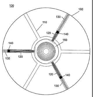
[0046] A top view drawing of an electro-active (EA) spectacle lens 100
manufactured by the
proposed methods is shown in FIG. 1. This lens includes an integration insert
110 possessing
transparent, thin film signal electrical leads 120 and battery electrical
leads 130, to which an
electro-active (EA) optical element 150 and integrated circuits 140 are
attached. FIG. 2 shows
the integration insert without any of the thin film electrical leads or
integrated circuits applied.
The central ring 180 and "arms" 190 of the integration insert 110 act to
provide physical support
when incorporating the EA element 150 within the bulk refractive optical
element 160 and
provide a platform for attaching transparent electrical leads 120 and 130 and
integrated circuits
140 which are needed to operate the EA element. The EA element may have planar
surfaces,
curved surfaces or may be designed such that one surface is planar and the
other is curved. In
most but not all cases these surfaces are equidistant from each other.
Integration insert 110
contains alignment edges 170 located within central ring 180 to aid aligning
of the insert with EA
element 150. The insert must be optically transparent (for obvious cosmetic
reasons) and have
the ability to conform to the various radii of curvature of a lens that exists
for different distance
vision prescriptions. If the insert did not conform to the radii of curvature
of a lens for a distance
prescription, a thicker lens would result which would be unacceptable to the
wearer. As such, the
insert can be either cut or stamped from flexible sheets of glass or plastic
whose thicknesses
range from 50 m to 150 m. Sheet glass is commercially available with
thicknesses'down to 30
8
CA 02636773 2008-07-10
WO 2007/081959 PCT/US2007/000549
m (Schott? D 263 T and AF 45) and many different types of plastics are
available in
comparable thicknesses. While the integration in ert is shown here as
comprising a central ring
180 with an opening and separate arms 190 extending radially from said ring,
the insert need not
be this shape. In certain other embodiments, the insert may take any form
which includes an
opening for an EA element and material peripheral to the opening for
supporting thin-film signal
electrical leads, thin-film battery electrical leads, and integrated circuits.
By way of example
only, the insert may be a flat toroidal shape, with a central opening and
alignment edges.
[0047] Electrical leads 120 and 130 can be made from thin films of transparent
conductive oxides
(e.g. ITO, ZnO, Sn02) or conducting polymers (e.g. polyaniline, PEDOT:PSS) and
are applied to
the surface(s) of the insert 110 as shown in FIG. 3. The electrical leads may
be added to the
insert by means of either additive or subtractive processes. Additive
processes would include (for
example) screen printing or thin-film deposition through a shadow mask of the
electrical lead
material. Subtractive processes would include (for example) either partially
or completely
coating the insert with the desired material and then removing the excess by
means of either a
patterned etch resist or a direct write laser ablation process. In embodiments
of the invention, the
thickness of the material from which the leads are constructed may be 1?m or
less and in
preferred embodiments, the thickness is 100 nm or less. In other embodiments
of the invention
the leads may be placed on both faces of the insert.
[0048] The electrical leads allow an integrated circuit (IC) 140, which
contains the drive
electronics for the EA element, to be directly mounted to the insert as
illustrated in FIG. 4. A
close-up view of one of the arms is shown in FIG. 5 where, by way of example
only, 2 power
supply (i.e. battery) electrical leads (1 voltage and 1 ground) 130 and 9
signal electrical leads (8
drive signals for each phase level and 1 ground) 120 are shown connected to
the IC. The IC is
capable of providing separate voltages to each signal electrical lead based
upon the desired phase
level. The number of signal electrical leads depends upon the configuration of
the EA element
(discussed below) and may be, by way of example only, as few as 3 or as many
as 34. The width
of the leads depends on the available space, the number of leads required, and
the width of the
inter-lead space required for electrical isolation. By way of example only,
leads 100 ?m wide
with 100 ?m spaces may be used for the signal electrical leads whereas 300 ?m
wide leads with
300 ? m wide spaces may be used for the battery electrical leads. The signal
electrical leads
connect to the EA element's patterned electrodes by means of an electrical
contact. In
9
CA 02636773 2008-07-10
WO 2007/081959 PCT/US2007/000549
embodiments of the invention in which the EA element is a diffractive lens
with patterned,
concentric ring electrodes, it is the relative size (radius and width) of the
patterned electrodes
within the elemeint that defines the optical add power of the diffractive
grating structure. The
separate amplitudes of the voltages applied by the IC to the separate
electrical signal leads (and
thus to the patterned electrodes) determine the phase profile produced in the
layer of liquid
crystal and as such, determine the diffraction efficiency (fraction of the
incident light that is
focused) of the EA element. As such, a single IC design with a single SKU
number assigned to it
may be used to drive any EA element regardless of the optical add power it
provides. In
embodiments of the invention in which the EA element is a pixelated, patterned
electrode device,
the optical power and/or aberration correction is completely dynamic and
determined by the
pattern of voltages addressed to the array of pixels. In embodiments of the
invention in which the
EA element is a modal lens, it is the amplitude of the voltage applied to the
high conductivity
ring electrode that defines the optical add power, where, generally, the
higher the applied voltage
the larger the amount of optical add power. In embodiments of the invention
where the EA
element is a surface relief optic, the optical power/aberration correction is
fixed by the pattenn
transferred into the substrate but the optic is made dynarnic by means of
voltage applied to create
refractive index matching and mismatching.
[0049] To facilitate the connection of the insert 110 to the external power
source, a small
electrical connector (not shown) may also be attached to the insert. Compared
to making contact
to the thin film battery electrical leads .130 after the lens is fully
assembled, such a connector
would be far more physically robust and would help reduce the number of
manufacturing steps.
Such a connector, if made from a combination of sufficiently soft materials
that are both
electrically insulating and conducting, could be designed to be machined flush
with the edge of
the lens using existing edging tools and still provide an acceptable
electrical connection. By way
of example only, the connector could be a small block of plastic with a
refractive index closely
matched to that of the bulk lens material that contains wires made from copper
(a soft metal) that
are bonded to the battery leads using appropriate means such as a conductive
adhesive. After the
bulk lens (also made from plastic) is formed around the insert and connector,
the machining step
typically used to form the outer peripheral edge of a finished lens would be
able to easily cut
through the small plastic block and the copper wires, exposing the wires for a
subsequent
connection to a power source.
CA 02636773 2008-07-10
WO 2007/081959 PCT/US2007/000549
[0050] The integration insert 110 has been designed with multiple mounting
positions such that
the IC 140 may be placed at various radial distances from the center of the EA
element 150 to
accoirunodate the varied sizes of available spectacle lens frames. Thus, there
will always be an
appropriate radial distance from the center of the EA element where the IC can
be mounted so
that it will not be cut off when the lens is edged to the proper size. Three
ICs are shown mounted
to the insert for illustration purposes only; in practice only one IC should
be required.
Furthermore, fabricating only a single insert with multiple IC mounting
positions reduces the
number of stock keeping units (SKUs).
[0051] The EA element 150 and its constitutive components are shown in FIGs.
6a-6c. The EA
element is comprised of substrates which, by way of example only, may be made
from inorganic
materials such as glass or sapphire or organic materials such as acrylates, a
class of materials
typically used to form ophthalmic lenses. In an embodiment of the invention, a
total of three
substrates may be used to construct the EA element. In such an embodiment, two
substrates 200
have photolithographically patterned transparent electrodes 220 on one surface
(FIG. 6b) and one
substrate 210 has a single continuous transparent electrode (FIG. 6c) on both
surfaces, which acts
as the reference (ground). In another embodiment of the invention only two
substrates are used.
In such an embodiment, one substrate 200 has photolithographically patterned
transparent
electrodes 220 on one surface (FIG. 6b) and one substrate 210 has a single
continuous transparent
electrode (FIG. 6c) on one surface, which acts as the reference (ground). As
discussed
previously, electrodes can be patterned as concentric rings to generate
optical add power (to
correct for presbyopia) or in an array of pixels to correct for any arbitrary
optical error of the eye,
including, by way of example only, presbyopia and higher-order aberrations.
[0052] In embodiments of the invention with patterned, concentric ring
electrodes 220, the EA
element provides optical add power whereby the patterned electrodes 220 act to
define a multi-
level diffractive lens structure in a thin layer of liquid crystal. When using
a multi-level
diffractive optic, each signal electrical lead is used to drive multiple
patterned concentric ring
electrodes so as to produce the correct phase profile in the layer of liquid
crystal. While only 10
patterned electrodes are shown for simplicity (FIG. 6a), a typical lens may
contain, by way of
example only, up to 3000 individual electrodes of varying widths from 1?rn to
100 ?m, by way
of example only. In embodiments of the invention with a pixelated EA element
(FIG. 8b), the
11
CA 02636773 2008-07-10
WO 2007/081959 PCT/US2007/000549
number of pixels could be, by way of example only, as few as 100 or as many as
1,000,000. The
size of each pixel varies and can fall within the range of 1?m to 1 mm, by way
of example only.
[0053] In another embodiment of the invention an alternate EA element 151 is
shown (FIG. 6e)
which uses two substrates 400 with surface relief optics (shown here, by way
of example only, as
diffractive lenses) 420 coated with a single continuous electrode (not shown)
instead of planar
substrates 200 with patterned electrodes 220. In this alternate embodiment,
surface relief optics,
which are well known in the art, generate the desired amount of optical power
and the layer of
liquid crystal is used as a dynamic refractive-index matching material. Under
a first applied
voltage the refractive index of the liquid crystal is substantially the same
as (matches) the
refractive index of the substrate 400 and there is substantially no
diffraction. Instead, incident
light only experiences a single refractive index as if the EA element were a
planar layer of
homogeneous material. Under a second applied voltage the refractive index of
the liquid crystal
is different from (mismatches) the refractive index of the substrate 400 and
there is diffraction of
the incident light due to the resulting phase difference generated by the
index mismatch. In a
preferred embodiment of the invention refractive index matching is achieved
when zero voltage
is applied to the EA element as this renders it fail safe (zero optical add
power under zero applied
voltage). A non fail-safe lens is undesirable as the sudden introduction of
optical power at an
inappropriate time (e.g. while driving) can be dangerous to the wearer.
Surface relief optics
which generate optical add power are shown by way of example only, in other
embodiments they
can be used to generate phase profiles -similar to those that can be generated
by a pixelated EA
element with pattemed electrodes.
[0054] Alternate EA element 151 is constructed from two substrates 400 with
surface relief
optics 420 coated with a single continuous electrode (FIG. 6f) and one
substrate 210 with a single
continuous transparent electrode (FIG. 6g) on both surfaces, which acts as the
reference (ground).
The one substrate with the single continuous transparent electrode on both
surfaces (FIG. 6g) is
identical to substrate 210 that is used for the EA element with patterned
electrodes. An exploded
view of FIG. 6e along the axis A-A is shown in FIG. 6h, where the surface
relief diffractive
structure is clearly visible. One benefit of this embodiment is that as the
inner surface of each
substrate now only contains a single continuous electrode, the number of
electrical contact points
230 is reduced to four, two to make the electrical ground connections and two
to make the drive
voltage connections. In another embodiment of the invention only two
substrates are used. In
12
CA 02636773 2008-07-10
WO 2007/081959 PCT/US2007/000549
such an embodiment, one substrate 400 has surface relief optics 420 on one
surface (FIG. 6f) and
one substrate 210 has a single continuous transparent electrode (FIG. 6g) on
one surface, which
acts as the reference (ground).
[0055] In yet another embodiment of the invention, alternate EA element 152 is
constructed from
two substrates 500 with modal lens electrodes (FIG. 6j) and one substrate 210
with a single
continuous electrode on both surfaces, which acts as the reference (ground),
(FIG. 6k). Modal
lens electrodes consist of a single, continuous circular electrode 520
comprising a low
conductivity material and a single, continuous ring electrode 521 comprising a
high conductivity
material. The one substrate with the single continuous transparent electrode
on both surfaces
(FIG. 6k) is identical to substrate 210 that is used for the EA element with
patterned electrodes.
An exploded view of FIG. 6i along the axis A-A is shown in FIG_ 61, where
electrical connection
between the low-conductivity electrode 520 and high-conductivity electrodes
521 is shown. One
benefit of this embodiment is that as the inrier surface of each substrate now
only requires a
single electrical contact to the high conductivity ring electrode, the number
of electrical contact
points 230 is reduced to four, two to make the electrical ground connections
and two to make the
drive voltage connections. Electrical connection between the contact points
230 and the high-
conductivity ring electrode 521 is made, by way of example only, by means of a
transparent thin-
film electrode or conductive adhesive lead (not shown). In another embodiment
of the invention
only two substrates are used. In such an embodiment, one substrate 500 has
modal lens
electrodes 520 and 521 on one surface (FIG. 6j) and one substrate 210 has a
single continuous
transparent electrode (FIG. 6k) on one surface, which acts as the.reference
(ground).
[0056] Substrates 200, 400 and 500 have electrical contact points 230 near the
periphery which
make connection to the patterned electrodes 220, 420 and 521, respectively,
using a system of
conductive thin-film buses (not shown) and which are designed to align with
the signal electrical
leads 120 placed on the integration insert 110. Tn embodiments of the
invention in which two
substrates 200, 400, or 500 are incorporated into the EA element, the insert
may have signal
electrical leads placed on both surfaces which may be used to make contact
with the electrical
contact points 230 on the surfaces of both substrates 200, 400 or 500. In such
an embodiment,
one integrated circuit 140 may be placed on each side of the integration
insert 110 or electrical
connection can be made from one integrated circuit to both sides of the insert
by means of
electrical vias in the insert. Electrical vias are well known in the art and
consist of physical
13
CA 02636773 2008-07-10
WO 2007/081959 PCT/US2007/000549
openings in a layer of electrically insulating material which contain
electrically conductive
materials to enable discrete electrical connections across the thickness of
the electrically
insulating material. Electrical connection between the reference (ground)
substrate and the
integration insert is made, by way of example only, by a wire bond or
conductive epoxy trace 231
as shown in FIGs. 7a-7b. The proper orientation of the EA element within the
integration insert
is facilitated by the alignment edges 171 along the periphery of the reference
substrate 210,
which register to the corresponding structures- 170 on the integration insert
110. Preferably, the
integration insert and the EA element are designed to have rotational symmetry
with respect to
their alignment edges. Thus, electrical connection between the EA element and
the integration
insert may be made along any of the integration insert's alignment edges 170
which has signal
electrical leads terminate near it and any of the EA element's alignment edges
171 which has
electrical contact points.
[0057] To assemble the EA element 150, every substrate surface containing an
electrode is
treated with liquid crystal alignment layers (not shown, but are well known in
the art) to induce a
given direction of liquid crystal alignment. Thus, substrate 200 will have the
surface containing
the patterned electrodes treated with a liquid crystal alignment layer and
substrate 210 will have
both surfaces containing the single continuous electrode treated with a liquid
crystal alignment
layer. Liquid crystal alignment layers are thin films (typically < 100 nm
thick) of a polyimide
material which are applied to 'those surfaces which come into direct contact
with liquid crystal.
The surfaces of these films are, prior to EA element assembly, rubbed or
buffed in one direction
with a cloth such as velvet (a technique well known in the art). When liquid
crystal molecules
come into contact with such a surface, the molecules preferentially lie in the
plane of the
substrate and are aligned in the direction in which the polyimide layer was
rubbed. This process
is the same for all EA elements regardless if concentric ring electrodes,
pixelated electrodes,
modal lens electrodes, or surface relief structures are used.
[0058] In embodiments of the invention in which nematic liquid crystal is
used, three substrates
must be used in order to overcome the fact that nematic liquid crystals are
polarization sensitive
(i.e. light of different polarizations experience different refractive indices
as they travel through
the material). Subsequent to preparing the alignment layers, the three
substrates are then stacked
to allow the formation of two liquid cells (a cell being both a layer of
liquid crystal and the two
substrate surfaces between which it is confined). For the sake of clarity, the
layers of liquid
14
CA 02636773 2008-07-10
WO 2007/081959 PCT/US2007/000549
crystal are not shown in the drawings. The two substrates with patterned
electrodes 200 are
placed on either side of the substrate containing the single continuous
electrode 210, such that the
substrate surfaces with patterned electrodes face the substrate surfaces with
the continuous
electrode. Thus, the inner surfaces of the two cells each posses a reference
electrode and a
patterned electrode. The substrates are stacked in such a way that within a
given cell, the
directions of liquid crystal alignment induced by the two alignment layers are
anti-parallel
(directions differ by 180?) but that the directions of alignment of one cell
are orthogonal to those
of the second cell. This anti-parallel and orthogonal arrangement of the
alignment layers enables
operation of an EA element with nematic liquid crystal in unpolarized ambient
light. An
assembled EA element according to this embodiment of the invention can be seen
in FIG 6a.
FIG. 6d shows an exploded view of FIG. 6a along the axis A-A. The polarization
sensitivity of
nematic liquid crystals is independent of all the aforementioned
configurations of the EA element
and the use of two, orthogonally aligned layers is required for all EA
elements regardless if
concentric ring electrodes, pixelated electrodes, modal lens electrodes, or
surface relief structures
are used.
[0059] In another embodiment of the invention the use of a polarization
insensitive cholesteric
liquid crystal would eliminate the need for a second layer of liquid crystal
and, if such were the
case, only two substrates, one with patterned electrodes and another with a
continuous reference
(ground) electrode, would be needed. Cholesteric liquid crystals are a class
of materials similar
to nematic liquid crystals in that their constituent molecules tend to orient
in a single direction,
but differ in that the preferred direction of orientation twists along a given
axis within the
material. If the twist pitch (distance along said axis over which the
preferred direction of
orientation rotates by 360?) is on the order of, or less than, the wavelength
of light, then the light
may see a refractive index that is nearly independent of its polarization. As
with an EA element
with nematic liquid crystal, alignment layers are placed on the substrate
surfaces containing
electrodes. However, it is no longer necessary to align the substrates such
that the alignment
layers are anti-parallel. Additionally, because there is only one cell, an
orthogonal relationship
between cells is not necessary or possible. In a preferred embodiment of the
invention,
polarization insensitive cholesteric liquid crystals are used in conjunction
with the alternate EA
element shown in FIGS. 6e - 6h which utilize surface relief diffractive
lenses. This embodiment
is preferred as it requires only two substrates (one substrate 400 and one
substrate 210), a single
layer of electro-active material, and two electrical contact points, greatly
simplifying the
CA 02636773 2008-07-10
WO 2007/081959 PCT/US2007/000549
fabrication of the EA element. This process is the same for all EA elements
regardless if
concentric ring electrodes, pixelated electrodes, modal lens electrodes, or
surface relief structures
are used.
[0060J The overall thickness of the fully assembled EA element should be less
than 200 m (and
be comparable to the thickness of the integration insert) so as to reduce the
thickness of the
finished EA spectacle lens. For example, when building a polarization
insensitive EA element
with two, 5 m layers of nematic liquid crystal, the thicknesses of the 3
individual substrates
should be less than 60 m (3 x 60 m + 2 x 5 m = 190 m). In a more preferred
embodiment of
the invention the total thickness of the EA element may be 600 ?m or less to
allow for easier
fabrication. For example, when building a polarization insensitive EA element
with two, 5 m
layers of nematic liquid crystal, the thicknesses of the 3 individual
substrates should be less than
196 gm (3 x 196 m + 2 x 5 m = 598 m). The fabrication of individual EA
elements of
various focal lengths (optical add powers) also helps to further streamline
the manufacturing
process. Fabricating the EA element separately from the integration insert
reduces the number of
SKUs as now there is no need to create a SKU number for each combination of
optical add power
and IC location; there only needs to be a SKU number for the insert, the IC,
and each optical add
power value, an additive as opposed to multiplicative calculation.
[0061 ] The assembled EA element is placed at the center of the integration
insert 110 such that
the electrical contact points 230 on the substrates align with the
corresponding electrical leads
120 on the integration insert 110 (FIG. 7a-7b), a process which is facilitated
by the alignment
edges 171 on the reference substrate 210 and the alignment edges 170 on the
integration insert.
Electrical connections between the EA element and the insert can be made by a
number of
methods including (but not limited to) conducting adhesives, metal bump-
bonding and wire
bonding. Incorporating the EA element into the insert can be accomplished in a
number of ways.
An example of an assembled EA element with patterned, concentric ring
electrodes incorporated
into an integration insert is shown in FIG. 8a. An example of an assembled EA
element with
patterned, pixelated electrodes incorporated into an integration insert is
shown in FIG. 8b. This
process is the same for all EA elements regardless if concentric ring
electrodes, pixelated
electrodes, modal lens electrodes, or surface relief structures are used.
[0062] In one embodiment of the invention with three substrates, the reference
substrate 210 is
placed at the center of the insert and electrical contact is made between the
reference substrate
16
CA 02636773 2008-07-10
WO 2007/081959 PCT/US2007/000549
and the ground signal electrical leaci. l tnen, tne substrates witn parternea
eiecrroaes /-vv dre
attached, by means of an optically transparent adhesive such as NOA65 (Norland
Products) to
either side of the reference substrate 210 such that the electrode surfaces
face each other. Before
the substrates are attached, liquid crystal alignment layers are applied and
the cells are oriented as
explained above. The cells could then, in no particular order, be filled with
liquid crystal and
connected, via contact points 230, to the signal electrical leads on the
insert. This process is the
same for all EA elements regardless if concentric ring electrodes, pixelated
electrodes, modal lens
electrodes, or surface relief structures are used.
[0063] In another embodiment of the invention with three substrates, only one
of the two cells
(comprising the reference substrate 210 and one substrate with patterned
electrodes 200) is
assembled (as explained above) and electrically connected to the insert.
Subsequently, the
second substrate with patterned electrodes 200 is properly oriented and
attached to the opposite
side of the reference substrate and electrical connections are made. In this
embodiment the cells
could be filled with liquid crystal as they are assembled or after both have
been assembled. This
process is the same for all EA elements regardless if concentric ring
electrodes, pixelated
electrodes, modal lens electrodes, or surface relief structures are used.
[0064] In another, less preferred embodiment of the invention with three
substrates, the EA
element, regardless of its configuration, is completely assembled and
incorporated within the
flexible integration insert by means of bending or otherwise temporarily
physically deforming the
insert such that the EA element will fit within the opening.
[0065] In embodiments of the invention utilizing an EA element incorporating a
polarization
insensitive cholesteric liquid crystal, only two substrates are required, one
with a reference
electrode and one with patterned electrodes. In such an embodiment,
incorporation of the two
substrate EA element is greatly simplified as the EA element may be fully
assembled before
hand, where making the electrical connections to the insert is the only
remaining processing step.
This process is the same for all EA elements regardless if concentric ring
electrodes, pixelated
electrodes, modal lens electrodes, or surface relief structures are used.
[0066] The use of multiple components in the assembly of the integration
insert will require the
use of ari encapsulating adhesive or resin to both physically stabilize the
fully assembled insert
(which includes the EA element) and to form at least one of the finished
surfaces of the final lens.
It should be pointed out that the use of the term finished lens blank denotes
an optic that is
17
CA 02636773 2008-07-10
WO 2007/081959 PCT/US2007/000549
tinished on both sides and has a defined optical power. A semi-finished lens
blank is finished on
one side and lacks a defined optical power. An unfinished lens blank could be
either semi
finished or have neither side fnished. The terfn wafer can mean either a thin
semi-finished lens
blank or a finished lens blank. Finally, the term blank denotes that such lens
article has not been
edged or shaped into the final shape of the spectacle lens frame.
[0067] It should be further pointed out that the finished lens is fabricated
in such a way as to
correct for the conventional optical errors of sphere and cylinder or in an
inventive approach, to
correct for higher order aberrations. The fabrication of lenses which correct
for conventional
refractive errors of sphere and cylinder is well known in the art. To correct
higher order
aberrations of the human eye, the optical power of the lens will be fabricated
to have localized
optical power changes that will correct for the higher order aberration or
aberrations specified in
terms of type, power, and position. In most cases, the higher order aberration
correction is
determined by way of a wave-front analysis of the eye of the wearer of said
finished electro-
active spectacle lenses. The higher order aberration correction can be
accomplished by
producing localized changes in optical power of said lens blank and can be
imparted by way of
machining an exposed, external surface to which the electro-active layer is
not affixed. It is to be
understood that machining can include the process of surfacing and polishing
the lens.
Alternatively, localized changes can be imparted by way of curing a thin resin
layer that is
contained within said lens blank such as to cause localized index changes in
the lens blank_ The
localized changes can also be imparted when adding the electro-active layer to
the lens blank by
imparting the localized changes by way of curing the surface-casting resin
layer between said
lens blank and around the electro-active layer. Higher order aberration
correction can also be
accomplished with the use of a pixilated optic as shown in FIG. 8b.
[0068] Two approaches for incorporating the integration insert 110 with the
bulk refractive
element 160 are shown in FIGs. 9a-9e and FIGs. l0a-10e. The first approach
utilizes a plastic,
finished lens blank 300 with a flat region 310 near the center (FIG. 9a) to
which the assembled
insert 110 is laminated with an optically clear adhesive (FIG. 9b). The flat
region 310 near the
center will help restrict any possible bending of the EA element 150, which
may distort the liquid
crystal layer and lead to reduced performance. This sub-assembly is then
inverted and placed
into a mold 330 that defines the other finished surface of the lens. The mold
330 is then filled
with a UV or heat sensitive resin 320 and cured (FIG. 9c). After the resin 320
is cured, the lens is
18
CA 02636773 2008-07-10
WO 2007/081959 PCT/US2007/000549
removed from the mold 330 (FIG. 9d) and is ready for any additional processing
required to fit it
into a suitable spectacle lens frame. Techniques for the "surface casting" of
optical quality
surfaces are known in the art. It should be noted that while the material from
which the finished
lens blank 300 or semi-finished lens blank 340 is manufactured may not be the
same material
used in the surface cast layer 320, the two materials should have
substantially the same refractive
index.
[0069] The lens blank employed in the above method may be either finished or
semi-finished.
Incorporating- the insert with a finished blank 300 eliminates the need for
any post-lamination
mechanical grinding/polishing of optical surfaces but requires knowledge of
the patient's
prescription and frame shape (i.e. a custom product). The use of semi-finished
blanks 340 (FIG
9e) will require a post-lamination mechanical grinding/polishing step but does
not require any
knowledge of the patient's prescription. This would be the preferred approach
as semi-finished
tenses could be sold directly to wholesale laboratories and in doing so, would
not interrupt the
established flow of goods and information from lens manufacturer to patient.
[0070] As an alternative to the lamination method, the integration insert 110
may be cast within a
volume of cured resin that forms the distance vision lens. Techniques for
casting whole lenses
from liquid resins are also known in the art. The casting of an EA lens can be
accomplished by
first mounting the arms 190 of the insert 110 to a rigid mounting ring/mold
gasket 400 as shown
in FIG. 10a. The rigid ring 400 is then mounted (temporarily) to a mold 420,
whose surface
defines one of the finished surfaces of the EA lens (FIG. lOb). A second mold
430 is then
mounted to the rigid ring 400 in a similar fashion such that a cavity is
formed, with the
integration insert 110 suspended between the two mold surfaces (FIG. lOc). The
cavity is then
filled with a suitable resin 410 and cured. After the resin 410 is cured the
molds 420 and 430 and
rigid ring 400 are removed and the resulting lens is ready for any additional
processing required
to fit it into a suitable spectacle lens frame (FIG. 10d). To facilitate the
manufacturing process,
the rigid mounting ring/mold gasket 400 may be made from an inexpensive,
injection moldable
material such that it is disposable. As with the lamination method, a molded
semi-finished blank
440 (FIG 10e) can be used instead of a finished mold blank. Either a finished
or semi-finished
EA lens may be produced with this method; with the production of a semi-
finished lens preferred
for the aforementioned reasons.
19
CA 02636773 2008-07-10
WO 2007/081959 PCT/US2007/000549
[0071] A benefit of these two approaches is that the parameters of the fully
assembled EA
component are both- independent of and insensitive to any requirements on the
patient's distance
and/or astigmatic vision correction. While a patient's prescription is
required to manufacture
finished lenses (by either lamination or casting) the rotational symmetry of
the insert allows it to
be oriented in such a way that the IC is placed in an aesthetically acceptable
location that is
independent of the patient's astigmatic axis. Manufacturing semi-finished
lenses (by either
lamination or casting, FIG. 9e and FIG. IOe) is even more forgiving as the
distance/astigmatic
correction is added after the lens is manufactured. The lack of correlation
between the near and
distance vision corrections and the rotational symmetry of the integration
insert allows well-
established lens manufacturing and processing technologies to be utilized with
only minor
modifications for the incorporation of the EA technology. The manufacture of
semi-finished
blanks by either of the previously mentioned methods allows the use of a
technique known as
free-forming to generate the finished lens from the semi-finished blank. Free-
forming is a form
of computer numerical control (CNC) machining used to grind and polish the
patient's
prescription into a surface of the semi-finished lens blank and is well known
in the art. Free
forming has the advantage that while it is commonly used to generate-surfaces
for distance'vision
correction, in certain embodiments of the current invention it can also be
used to generate
surfaces for the correction of higher-order aberrations.
[0072] While these two methods offer many benefits for manufacturing EA
spectacle lenses,
their success depei2ds on the ability to match the refractive indices of all
the optical materials and
components involved. If the refractive indices are not all equal (within a
margin of error of ?
0.02) then the edges of the-integration insert and EA element may be visible
and the product will
not be acceptable to the patient. Fortunately, there are many optical
materials that can exhibit a
wide range of refractive index values and 'are compatible with different
processing technologies.
One limitation however, is that the use of conventional photolithography (and
its associated
organic solvents) to define the patterned EA electrodes make inorganic
materials better
candidates for substrate materials. By way of example only, suitable inorganic
materials include
glass and sapphire where glass would be preferred over sapphire due to the
high cost of sapphire.
Still, with proper care and selection of solvent used in the processing of the
electrodes, organic
materials such as films formed from acrylates may be used to make EA elements.
Glass
manufacturers for the optics industry such as Schott, Hoya, and Ohara supply
glasses with
refractive indices that range from slightly below 1.50 to slightly above 2.00,
values which
CA 02636773 2008-07-10
WO 2007/081959 PCT/US2007/000549
overlap well with the needs of the ophthalmic industry. Refractive indices of
various monomers
(resins) and polymers (plastics) also cover a wide range of values but do not
currently achieve
values as high as those of the optical glasses. Typical "large" refractive
indices for commercial
optical resins and plastics are on the order of 1.60 to 1.70 - values which
are primarily driven by
the ophthalmic industry. Given the broad range of overlap in refractive index
values for the
various materials the index matching requirement appears to present no major
challenges. - There
are however, preferred ranges for the refractive index. Many optical materials
tend to have
refractive indices near to 1.50 and in one embodiment of the invention; the
refractive index of the
individual components is matched to a value near to 1.50. If polarization
insensitive cholesteric
liquid crystals are used, which have a refractive index of approximately 1.66,
then in another
embodiment of the invention the refractive index of the individual components
is matched to a
value near to 1.66. In an effort to reduce the number of individual components
that need to be
index matched, in certain embodiments of the invention, one of the substrates
used to construct
the EA element may be replaced by either a finished lens blank or a semi-
finished lens blank
when the lamination method of lens construction is used. In such an
embodiment, the
construction of the complete integration insert will include the finished or
semi-finished lens
blank.
[0073] The above outlines a method for manufacturing EA spectacle lenses that
correct for
presbyopia by the use of a liquid crystal based dynamic, electro-active lens
embedded within a
conventional spectacle lens that provides distance vision correction. While
this invention is
targeted at correcting presbyopia, the methods presented could be used to
construct spectacle
lenses that correct for other vision errors, such as higher order aberrations
of the eye.
21