Note: Descriptions are shown in the official language in which they were submitted.
CA 02636776 2008-07-10
DESCRIPTION
Method of Manufacturing Silicon Carbide Semiconductor Device
TECHNICAL FIELD
The present invention relates to a method of manufacturing a silicon carbide
semiconductor device such as an MOSFET, having a gate insulating film low in
interface
state density.
BACKGROUND ART
Semiconductor devices such as a transistor and a diode formed with a silicon
carbide substrate (SiC substrate) composed of silicon (Si) and carbon (C)
bonded to
each other at a composition ratio of 1:1 have been expected to go into actual
use as
power devices. As silicon carbide is a wide bandgap semiconductor, its
breakdown
electric field is higher than that of silicon by one order of magnitude.
Accordingly,
even if a depletion layer at a pn junction or a Schottky junction has a
smaller thickness, a
high peak inverse voltage can be maintained. Here, as use of the silicon
carbide
substrate permits smaller thickness of the device and higher doping
concentration,
implementation of a power device having a low ON resistance, a high withstand
voltage,
and low loss has been expected. It is noted that the silicon carbide substrate
herein
encompasses any substrate obtained by epitaxially growing a silicon carbide
crystal layer
on a substrate composed of silicon carbide crystals or a material different
from silicon
carbide.
Meanwhile, as compared with an MOSFET (Metal Oxide Semiconductor Field
Effect Transistor) including a silicon substrate, an MOSFET including the
silicon carbide
substrate is disadvantageous in poor characteristics of a silicon oxide film
serving as a
gate insulating film, for the following reasons. Basically, as a large amount
of carbon
remains in a thermal oxidation film on the silicon carbide substrate, C-C
bonds or
dangling bonds are present, and consequently, interface state density in an
interface
-l-
CA 02636776 2008-07-10
region between the thermal oxidation film and a silicon carbide layer is high.
For addressing such a disadvantage, according to Japanese National Patent
Publication No. 2004-511101 (Patent Document 1), for example, lower interface
state
density in an interface region between an oxide layer and a silicon carbide
layer is
achieved by oxidizing the silicon carbide layer in dinitrogen monoxide (N20)
and
annealing the oxide layer on the silicon carbide layer in an N20 atmosphere.
Patent Document 1: Japanese National Patent Publication No. 2004-511101
DISCLOSURE OF THE INVENTION
PROBLEMS TO BE SOLVED BY THE INVENTION
According to Patent Document 1, nitrogen monoxide (NO) generated as a result
of thermal decomposition through annealing in N20 inactivates dangling bond of
Si, C
that is present in the interface region between an oxide film (oxide layer)
and a
semiconductor layer. Accordingly, the interface state serving as electron trap
is
lowered and carrier mobility is improved. According to the technique in Patent
Document 1, however, reaction between N20 and SiC should be caused at a
temperature of 1100 C or higher, and therefore Patent Document 1 is
disadvantageous
in poor throughput due to a long time required for temperature increase and
decrease in
an annealing furnace as well as in difficulty in maintaining uniformity of a
temperature
within a wafer.
An object of the present invention is to provide a method of manufacturing a
silicon carbide semiconductor device having low interface state density with
high
throughput.
MEANS FOR SOLVING THE PROBLEMS
A method of manufacturing a silicon carbide semiconductor device according to
the present invention includes: an oxide film forming step of forming an oxide
film
serving as a gate insulating film on a silicon carbide layer formed on a
substrate; and a
plasma exposure step of exposing the oxide film to plasma generated by using a
gas
containing at least any one of nitrogen element (N) and oxygen element (0),
after the
-2-
CA 02636776 2008-07-10
oxide film forming step.
According to this method, functions such as inactivation of a dangling bond by
an N atom and breaking of C-C bond by an 0 atom are attained, and therefore,
interface
state density in an interface region between an oxide film and a silicon
carbide layer can
be lowered through treatment at a relatively low temperature. In addition, as
higher
uniformity of plasma treatment within a wafer is more likely in the plasma
exposure step
than in annealing treatment, variation in the interface state density is also
smaller.
Therefore, in addition to improvement in channel mobility and lowering in a
leakage
current in an MOSFET or the like, variation in a threshold voltage of the
MOSFET or
the like is also smaller. Moreover, as the plasma exposure step can be
performed at a
relatively low temperature, throughput is also improved.
In the method of manufacturing a silicon carbide semiconductor device above,
in
the plasma exposure step, at least one gas selected from among a gas
containing
nitrogen molecules (N2), a gas containing oxygen molecules (OZ), and a gas
containing
ozone (03) is preferably employed as the gas containing at least any one of
nitrogen
element and oxygen element. Alternatively, a gas containing nitrogen element
and
oxygen element is preferably employed as the gas containing at least any one
of nitrogen
element and oxygen element. Here, at least one gas selected from a gas
containing
dinitrogen monoxide (N20) and a gas containing nitrogen oxide (NOx) is
preferably
employed as the gas containing nitrogen element and oxygen element.
In the method of manufacturing a silicon carbide semiconductor device above,
in
the oxide film forming step, a silicon oxide film is preferably formed as the
oxide film by
heating the silicon carbide layer in an atmosphere containing at least oxygen
element.
In forming the gate insulating film, by forming the silicon oxide film through
thermal
oxidation in which the silicon carbide layer is heated to a high temperature
in an
atmosphere containing at least oxygen element, information on a crystalline
state of the
underlying silicon carbide layer is taken over to the silicon oxide film. The
gate
insulating film well adapted to the underlying layer is thus obtained. Here, a
-3-
CA 02636776 2008-07-10
temperature for thermal oxidation treatment is preferably in a range from at
least
1250 C to at most 1400 C.
In the oxide film forming step, the oxide film is preferably formed with
chemical
vapor deposition (CVD). In forming the gate insulating film, by forming the
oxide film
with CVD, the gate insulating film relatively low in the interface state
density in the
region of interface with the underlying silicon carbide layer is obtained.
The method of manufacturing a silicon carbide semiconductor device preferably
further includes the step of planarizing the silicon carbide layer with
chemical mechanical
planarization (CMP) prior to the oxide film forming step. By planarizing the
silicon
carbide layer with CMP prior to forming the gate insulating film, distribution
of the
interface state density is made uniform, and the silicon carbide semiconductor
device
smaller in variation in the threshold voltage is obtained.
EFFECTS OF THE INVENTION
According to the method of manufacturing a silicon carbide semiconductor
device of the present invention, the silicon carbide sen-&onductor device
having low
interface state density in the interface region between the gate insulating
film and the
silicon carbide layer can be obtained.
BRIEF DESCRIPTION OF THE DRAWINGS
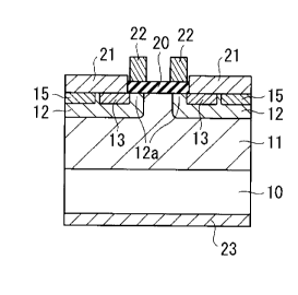
Fig. I is a cross-sectional view showing a step of manufacturing an MOSFET in
an embodiment.
Fig. 2 is a cross-sectional view showing a step of manufacturing the MOSFET in
the embodiment.
Fig. 3 is a cross-sectional view showing a step of manufacturing the MOSFET in
the embodiment.
Fig. 4 is a cross-sectional view showing a step of manufacturing the MOSFET in
the embodiment.
Fig. 5 is a cross-sectional view showing a step of manufacturing the MOSFET in
the embodiment.
-4-
CA 02636776 2008-07-10
Fig. 6 is a cross-sectional view showing a step of manufacturing the MOSFET in
the embodiment.
Fig. 7 is a perspective view schematically showing a structure of a plasma
apparatus used in the embodiment.
Fig. 8 illustrates data showing difference in dependency of channel mobility
on a
gate voltage, depending on whether plasma treatment is performed or not.
DESCRIPTION OF THE REFERENCE SIGNS
4H-SiC substrate; 11 epitaxially grown layer; 12 p well region; 12a channel
region; 13 source region; 15 p+ contact region; 20 gate insulating film; 21
source
10 electrode; 22 gate electrode; 23 drain etectrode; 50 plasma apparatus, 51
chamber; 52
tunnel; 53 upper electrode; 54 lower electrode; 61 wafer; and 62 wafer
carrier.
BEST MODES FOR CARRYING OUT THE INVENTION
(Embodiment)
Figs. 1 to 6 are cross-sectional views showing steps of manufacturing an
MOSFET representing a silicon carbide semiconductor device in an embodiment.
Though Figs. I to 6 show solely two transistor cells representing a part of a
vertical
MOSFET, a large number of transistor cells are integrated to configure one
vertical
MOSFET.
In the step shown in Fig. 1, an n-type 4H (hexagonal)-SiC (4 represents the
number of layers stacked in one period) substrate 10, for example, having a
resistivity of
0.02f2cm and a thickness of 4004m, and having a (0001) face at an off angle of
approximately 8 in [11-20] direction as a main surface is prepared. Then,
using CVD
epitaxial growth including in-situ doping, an epitaxially grown layer 11, for
example,
containing an n-type dopant in a concentration of approximately 5x1015cm 3 and
having
a thickness of approximately 10 m is grown on 4H-SiC substrate 10. An
outermost
surface of epitaxially grown layer 11 immediately after epitaxial growth has
an average
surface roughness Ra, for example, of approximately 0.2nm to 0.3nm. It is
noted
herein that an individual orientation and an individual face are shown with []
and ()
-5-
CA 02636776 2008-07-10
respectively.
Thereafter, in the step shown in Fig. 2, using ion implantation, a p well
region 12,
for example, containing a p-type dopant in a concentration of approximately I
x 10"cm-3
and having a thickness (depth) of approximately 1.0 m is formed in a part of a
surface
portion of epitaxially grown layer 11. Further using ion implantation, a
source region
13, for example, containing an n-type dopant in a concentration of 1 x 1019cm
3 and
having a thickness (depth) of approximately 0.3 m and a p+ contact region 15,
for
example, containing a p-type dopant in a concentration of 5x 1019cm 3 and
having a
thickness (depth) of approximately 0.34m are formed in each part of the
surface portion
of p well region 12. Here, the temperature of 4H-SiC substrate 10 and
epitaxially
grown layer 11 during ion implantation is set, for example, to 500 C.
Thereafter, an
abrasive mainly containing colloidal silica is used to perform CMP (chemical
mechanical
planarization), to thereby remove the surface portion of the substrate, for
example, by
approximately lnm to 5nm. The outermost surface of epitaxially grown layer 11
immediately after CMP has average surface roughness Ra, for example, in a
range from
approximately 0. inm to 0.5nm. Though not shown, in general, after these
steps, a
sacrificial oxide film is formed on the substrate using thermal oxidation, and
thereafter
the sacrificial oxide film is removed, and then the process proceeds to a next
step.
Thereafter, in the step shown in Fig. 3, for example, using thermal oxidation,
a
gate insulating film 20 formed as the silicon oxide film having a thickness of
approximately 50nm is formed on 4H-SiC substrate 10. Here, gate insulating
film 20 is
preferably formed through heating to a high temperature in an atmosphere
containing at
least oxygen element (0). Here, for example, 02, 03, N20, and the like may be
employed as the gas containing oxygen element. Through heating in the
atmosphere
containing oxygen element, an oxide film higher in quality than a film formed
with
sputtering or CVD can be obtained. Heating to a high temperature in a range
from at
least 1250 C to at most 1400 C is preferably performed. Heating to a high
temperature not lower than 1250 C can bring about lower interface state
density at an
-6-
CA 02636776 2008-07-10
interface between gate insulating film 20 and each layer within epitaxially
grown layer 11
(in particular, p well region 12). Heating to a high temperature not higher
than 1400 C
can suppress roughness of the surface of each layer within epitaxially grown
layer 11.
By performing thermal oxidation in the atmosphere containing oxygen element
and
nitrogen element, the interface state density at the interface between gate
insulating film
20 and each layer within epitaxially grown layer 11 (in particular, p well
region 12) can
also be lowered. By thus employing the gas containing nitrogen element and
oxygen
element (such as N20 and NO), the following function and effect is obtained,
as
compared with oxidation using solely oxygen element. Specifically, as
remaining
carbon from which the interface state originates is nitrided to attain a
passivation
function, further lower interface state density can be achieved.
Instead of thermal oxidation, for example, CVD (chemical vapor deposition)
may be employed. As the underlying silicon carbide layer is hardly altered in
CVD,
gate insulating film 20 achieving relatively low interface state density in
the region of
interface with the underlying silicon carbide layer is obtained. Therefore, as
far as only
an effect to lower the interface state density is concerned, CVD is preferred.
Thereafter, in the step shown in Fig. 4, with the use of a barrel type plasma
apparatus, a gas containing at least any one of nitrogen element and oxygen
element is
employed to generate plasma for plasma treatment of gate insulating film 20
(plasma
exposure step). In the plasma exposure step, for example, at least one gas
selected
from among a gas containing N2, a gas containing OZ, and a gas containing 03
is
employed as the gas containing at least any one nitrogen element and oxygen
element.
Thus, passivation or removal (elimination) of carbon remaining at the
interface between
the oxide film and each layer within epitaxially grown layer 11 can be
achieved.
Alternatively, for example, a gas containing nitrogen element and oxygen
element is
employed as the gas containing at least any one of nitrogen element and oxygen
element.
By doing so, passivation or removal (elimination) of carbon remaining at the
interface
between the oxide film and each layer within epitaxially grown layer 11 can
also
-7-
CA 02636776 2008-07-10
similarly be achieved. Here, for example, at least one gas selected from a gas
containing N2 and a gas containing NOx is employed as the gas containing
nitrogen
element and oxygen element. By doing so, passivation or removal (elimination)
of
carbon remaining at the interface between the oxide film and each layer within
epitaxially
grown layer 11 can also similarly be achieved. If the gas containing nitrogen
element
and oxygen element is employed, for example, a partial pressure (ratio)
between
nitrogen element and oxygen element can be set to 1:1.
The plasma exposure step is not particularly limited, so long as plasma is
generated by using the gas containing at least any one of nitrogen element and
oxygen
element. The gas containing at least any one of nitrogen element and oxygen
element
may further contain, for example, hydrogen or the like.
Fig. 7 is a perspective view schematically showing a structure of a plasma
apparatus 50 used in the embodiment. Plasma apparatus 50 includes a chamber 51
formed with a quartz tube or the like, a tunnel 52 formed with an aluminum
mesh tube
or the like provided in chamber 51, an upper electrode 53 attached to a
ceiling portion
of chamber 51, and a lower electrode 54 attached to a bottom portion of
chamber 51.
Upper electrode 53 is connected to a high-frequency power supply with a
matching unit
55 being interposed, and lower electrode 54 is connected to ground. A
plurality of
wafers 61 vertically placed on a wafer carrier 62 are arranged in tunnel 52.
In the present embodiment, for example, plasma is generated under such
conditions as power of 300W and frequency of 13.56MHz, while a gas obtained by
diluting NZU with a nitrogen gas to a concentration of approximately 10 volume
%
flows through chamber 51. For example, the temperature in chamber 51 is set to
approximately 100 C and a time period during which exposure to plasma is
performed is
set to approximately 60 minutes.
Thereafter, in the step shown in Fig. 5, a portion of gate insulating film 20
located above source region 13 and p+ contact region l 5 is removed, and
thereafter, a
source electrode 21 formed by a nickel (Ni) film having a thickness of
approximately
-8-
CA 02636776 2008-07-10
0.1 m is formed in a region from which gate insulating film 20 has been
removed, for
example, with a lift-off method.
Thereafter, in the step shown in Fig. 6, for example, by performing heat
treatment at a temperature of 975 C for 2 minutes in an argon (Ar) atmosphere,
a
contact characteristic between Ni composing source electrode 21 and a drain
electrode
23 and silicon carbide composing the underlying layer (source region 13, p+
contact
region 15 and 4H-SiC substrate 10) is changed from Schottky contact to Ohmic
contact.
Thereafter, a gate electrode 22 composed of Al is formed on gate insulating
film 20,
spaced apart from source electrode 21.
Through the manufacturing steps above, an n-channel vertical MOSFET
attaining a function as a power device is formed. In the vertical MOSFET, a
region
located in the uppermost portion of p well region 12 and under gate electrode
22 with
gate insulating film 20 being interposed attains a function as a channel
region 12a.
When the MOSFET turns on, the current supplied from drain electrode 23 flows
in the
vertical direction from 4H-SiC substrate 10 to the uppermost portion of
epitaxially
grown layer 11, and thereafter the current reaches source region 13 through
channel
region 12a in the uppermost portion of p well region 12. Here, in channel
region 12a,
electrons, i.e., carriers, run from source region 13 toward the uppermost
portion of
epitaxially grown layer 11. Mobility of electrons in channel region 12a refers
to
channel mobility.
In the step of forming the gate oxide film shown in Fig. 3 of the present
embodiment, CO or CO2 volatilizes as a result of bonding between C atoms in
epitaxially grown layer 11 (SiC layer) and 0 atoms, while a silicon oxide film
(Si02) is
formed as a result of bonding between Si atoms with 0 atoms. Here, unlike
thermal
oxidation at the surface of an Si layer, a large number of C atoms remain
after thermal
oxidation treatment of the surface of the SiC layer. Accordingly, a large
number of
dangling bonds of Si, C or C-C bonds representing bonding between C atoms are
present in the interface region between the gate oxide film and the silicon
carbide layer.
-9-
CA 02636776 2008-07-10
Consequently, a large number of interface state densities are present in a
region around
the interface between the gate oxide film and the silicon carbide layer.
Here, by exposing gate insulating film 20 to plasma generated by using the gas
containing oxygen element, a function of breaking of C-C bond by 0 atom is
attained.
In addition, by exposing gate insulating film 20 to plasma generated by using
the gas
containing nitrogen, a function to inactivate the dangling bond of Si, C
(termination
function) is attained. Any of these functions contributes to lower interface
state density
in the interface region between gate insulating film 20 and channel region
12a.
Consequently, channel mobility of the MOSFET is improved and leakage current
is also
decreased. In particular, in the present embodiment, as the gate insulating
film is
exposed to plasma generated by using the gas containing N20 which is the gas
containing oxygen and nitrogen, the function to break C-C bond and the
function to
inactivate the dangling bond are both attained, a function to lower the
interface density
is further noticeable.
Fig. 8 illustrates data showing difference in dependency of channel mobility
on a
gate voltage, depending on whether plasma treatment is performed or not. Data
curves
L1 and L2 in Fig. 8 represent channel mobility in an MOSFET sample (thickness
of gate
insulating film of 60nm) that has been subjected to plasma treatment (in the
case of this
sample, N2 plasma treatment) after the gate insulating film is formed and in
an MOSFET
sample (thiclcness of gate insulating film of 60nm) that has simply been
subjected to
thermal oxidation in Oz atmosphere to form the gate insulating film. Here, the
MOSFET samples were manufactured under the conditions described previously in
connection with the steps shown in Figs. 1 to 6. Here, average surface
roughness Ra
of epitaxially grown layer 11 was l Onm, average surface roughness Ra of the
outermost
surface of epitaxially grown layer 11 immediately after CMP was 0.5nm, and
gate
insulating film 20 was formed with thermal oxidation at 1300 C by using OZ as
the gas
containing oxygen element, or in the plasma exposure step, it was formed by
using the
gas obtained by diluting NZO with the nitrogen gas to a concentration of 10
volume %.
-10-
CA 02636776 2008-07-10
As shown in the figure, it can be seen that channel mobility noticeably
improved by
performing plasma treatment.
In addition, in the plasma treatment step shown in Fig. 4, the treatment
temperature is set to approximately 100 C, and treatment at a high temperature
around
1100 C is not necessary as in the technique of Patent Document 1. Therefore,
high
throughput can also be maintained.
Moreover, according to the technique of Patent Document 1, as the treatment is
performed at a high temperature around 1100 C, it is difficult to maintain
uniform
temperature distribution in the wafer, and variation in the interface state
density within
the wafer is significant. In contrast, according to the present invention,
uniform
treatment of the wafer with plasma can relatively easily be performed. As
uniformity of
the interface state density within the wafer is thus also high, variation in
the threshold
voltage of the MOSFET can be made smaller.
It is noted that data curves L I and L2 shown in Fig. 8 were plotted in a
graph by
calculating mutual conductance based on characteristics of a gate voltage and
a drain
current when a drain voltage of 0.1 V was applied and by finding field effect
mobility.
In the step of manufacturing an MOSFET according to the present embodiment,
the gas containing N20 was employed as the atmosphere for plasma treatment.
Here,
by employing the gas containing at least any one of nitrogen element and
oxygen
element, the interface state density present in the interface region between
gate
insulating film 20 and epitaxially grown layer I 1 can be lowered, and an
effect of the
present invention can thus be achieved. Specifically, a gas containing N2, a
gas
containing O2 or 03, a gas containing NOx, a gas containing nitrogen element
and
oxygen element, and the like are exemplary gases containing at least any one
of nitrogen
element and oxygen element. By employing these gases, plasma containing at
least any
one of oxygen element and nitrogen element can be generated.
A barrel type plasma generation apparatus is more advantageous as a plasma
generation apparatus than a parallel plate type plasma generation apparatus,
because
- 11 -
CA 02636776 2008-07-10
damage to a gate insulating film and the like is less likely. Damage can be
suppressed
also by employing ICP (Inductively Coupled Plasma).
In the step shown in Fig. 2, thermal oxidation is preferably performed at a
temperature in a range from at least 1250 C to at most 1400 C. This is
because, as the
temperature is higher, an effect to lower the interface state density is
greater. Here, an
atmosphere containing O2, an atmosphere containing NO2, an atmosphere
containing
N20, or the like may be selected for use as the atmosphere.
(Other embodiments)
The structure in the embodiment of the present invention disclosed above is by
way of illustration and the scope of the present invention is not limited by
the scope of
the description. The scope of the present invention is defined by the terms of
the
claims, and is intended to include any modifications within the scope and
meaning
equivalent to the terms of the claims.
In the embodiment above, an example in which the silicon carbide semiconductor
device according to the present invention is applied to an MOSFET (DMOSFET)
has
been described, however, the silicon carbide semiconductor device according to
the
present invention is also applicable to a VMOSFET, a LIMOSFET, an IGBT, and
the
like.
In addition, in the embodiment above, an example in which the present
invention
is applied to an inversion mode MOSFET has been described, however, the
present
invention is applicable also to an accumulation mode MOSFET. Moreover, in the
embodiment above, an example in which the present invention is applied to a
vertical
MOSFET has been described, however, the present invention is applicable also
to a
lateral MOSFET. Here, the drain region opposed to the source region with the
channel
region being interposed is formed in the surface portion of the epitaxially
grown layer.
The substrate in the present invention is not limited to a 4H-SiC substrate,
and
an SiC substrate of a poly type different from 4H poly type, such as a 6H-SiC
substrate
(the number of layers stacked in one period is 6) or a substrate made of a
material
-12-
CA 02636776 2008-07-10
different from those for the SiC substrate, such as an Si substrate, may be
adopted.
For example, by applying the present invention also to a silicon carbide
semiconductor
device including a 3C-SiC epitaxially grown layer hetero-epitaxially grown on
an Si
substrate, an MOSFET small in variation in a threshold voltage or a Schottky
diode of
high withstand voltage can be obtained.
INDUSTRIAL APPLICABILITY
The silicon carbide semiconductor device according to the present invention
may
be utilized for an MOSFET, an IGBT, and the like used as a power device or a
high-
frequency device.
-13-