Note: Descriptions are shown in the official language in which they were submitted.
CA 02636930 2014-01-20
WO 2007/082059
PCT/US2007/000813
WIDEBAND OPTICAL COUPLING INTO THIN SO! CMOS PHOTONIC
INTEGRATED CIRCUIT
Technical Field
The present invention relates to an apparatus for providing coupling into and
out of
a thin (i.e., sub-micron dimensioned) optical waveguide and, more
particularly, to the use
of reference planes and lensing elements to provide coupling between a fiber
or lens and a
thin waveguide.
Background of the Invention
A common prior art technique for coupling light from an external source to a
silicon waveguide is to cleave or polish end facets on both the waveguide and
the mating
fiber termination. Examples of fiber terminations include, but are not limited
to:
multimode or single-mode fibers with small or zero cleave/polish angles, and
specially-
shaped or lensed single-mode fibers that produce spot sizes as small as 1.5
m. The fiber
termination is aligned to allow maximum light transmission through the
waveguide, and
then fixed in position. Anti-reflection (AR) coatings can be used on both the
fiber
termination and the waveguide facet to reduce the Fresnel losses. In all of
these prior art
arrangements, the input and output ports are necessarily located at edge
facets of the
waveguiding-containing wafer die, significant restrictions on device geometry
(e.g.,
topology and/or size) are imposed by using this prior art edge coupling
constraint.
Another factor associated with optical coupling is the development and use of
extremely "thin" waveguides formed within the SOI layer of an SOI-based opto-
electronic
arrangement. For the purposes of the present invention, a "thin" waveguide is
defined as
having a typical width on the order of approximately 0.5 jam and a typical
thickness on the
order of approximately 0.15 m. In the past, "nanotapers" or "inverse tapers"
have been
successfully used with thin waveguides. However, this success has been shown
only within
research/development environments, where there is careful control over
fabrication
conditions.
1
CA 02636930 2008-07-02
WO 2007/082059 PCT/US2007/000813
Thus, a need remains in the art for a manufacturable, high efficiency optical
coupling arrangement for providing permanent coupling of lasers and fibers
into thin, SOT-
based optical waveguides as utilized will be required for high volume
production of opto-
electronic products.
Summary of the Invention
The need remaining in the art is addressed by the present invention, which
relates
to an apparatus for providing coupling into and out of a thin (i.e., sub-
micron
dimensioned) optical waveguide formed in the surface SOT layer of an SOI
structure and,
more particularly, to the use of reference planes within the SOI structure
itself and
associated lensing elements to provide coupling between a fiber or laser and a
thin
waveguide.
In accordance with the present invention, a defined interface within an SOI
structure (such as, for example, the interface between the silicon substrate
and the
overlying buried oxide (BOX) layer) is utilized as a reference plane for the
coupling
arrangement. The thin waveguide is formed within the SOI layer and terminates
at a
sidewall formed within the SOT structure, with a lensing arrangement utilized
to provide
coupling between the input device and the waveguide.
In one embodiment of the present invention, a separate lens element is
disposed
between the light source (either fiber or laser) and the sidewall termination
of the thin
waveguide. The lens is held within a fixture disposed in a trench that has
been etched into
the SOI structure. The fixture itself includes a reference surface that is
associated with the
SOT-based reference plane so that the lens will be in optical alignment with
the thin
waveguide when the fixture is placed in the trench. In an "active alignment"
configuration
of this embodiment, the lateral displace of the lens fixture with respect to
the waveguide
termination can be adjusted by moving the fixture along the lateral extent of
the trench
until maximum optical coupling is obtained. Permanent attachment is made once
maximum coupling is achieved.
In an alternative embodiment, a lensing arrangement may be directly integrated
with the optical source, such as a lensed fiber or a laser comprising an
integral lens. In the
case of a lensed fiber, the fiber is first be positioned within a separate
block component
(preferably a silicon block) that is mounted over the SOT structure. The
silicon block is
formed to include an accurately-positioned V-groove that will support the
fiber such that
2
CA 02636930 2008-07-02
WO 2007/082059 PCT/US2007/000813
the core is in the desired position to provide coupling to the thin waveguide.
The silicon
block is "flip chip" attached to the SOI structure to form the permanent
coupling
arrangement, using the substrate/BOX reference plane for optical alignment
between the
fiber's core and the thin waveguide.
In any of the embodiments of the present invention, a portion of the in-
coupled
signal propagating along the thin waveguide may be tapped off and used to as
an active
feedback signal to adjust the alignment between the laser/fiber and thin
waveguide until
maximum coupling has been achieved. Additionally, the same types of alignment
arrangements may be used to out-couple a signal propagating along a thin
waveguide into
an output fiber, or other optical output device (such as, for example, a
photodiode).
Other and further embodiments and features of the present invention will
become
apparent during the course of the following discussion and by reference to the
accompany
drawings.
Brief Description of the Drawings
Referring now to the drawings,
FIG. 1 is an isometric view of an exemplary SOI structure including both a
fiber-
based coupling arrangement and a laser-based coupling arrangement formed in
accordance
with the present invention;
FIG. 2 is an enlarged side view of an exemplary fiber coupling arrangement
formed in accordance with the present invention;
FIG. 3 is an exploded isometric view of the silicon block portion of the fiber
coupling arrangement and an associated optical fiber;
FIG. 4 is an isometric view of the silicon block of FIG. 3, with the fiber
positioned
within the block's V-groove;
FIG. 5 is an isometric view of the silicon block of FIG. 4 in place over an
SOT
structure including a thin waveguide to-which the fiber is to be aligned;
FIG. 6 is a simplified top view of an exemplary laser coupling arrangement
formed
in accordance with the present invention;
FIG. 7 is a side view of an exemplary lensing fixture of the invention,
showing in
particular the configuration of the reference surface and associated lensing
component;
3
CA 02636930 2008-07-02
WO 2007/082059
PCT/US2007/000813
FIG. 8 is a side view of the laser coupling arrangement of the present
invention,
illustrating the optical output from a laser source 24 as passing through a
lensing
component and being focused into a thin SOI waveguide; and
FIG. 9 is a top view of an exemplary arrangement of the present invention in
the
form of both an input coupling arrangement and an output coupling arrangement.
Detailed Description
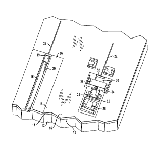
FIG. 1 is an isometric view of an exemplary SOT structure 10 formed to include
both a fiber coupling arrangement and a laser coupling arrangement of the
present
invention. It is to be understood that any number of fiber-based couplings
and/or laser-
based couplings may be utilized on a given SO! structure. The pair of
couplings is shown
here only for the sake of discussion and explanation.
As shown, SOI structure 10 comprises a silicon substrate 12, a buried oxide
(BOX)
layer 14 and a sub-micron thick, single crystal silicon surface layer 16
(hereinafter referred
to as "SOT layer 16"). It is an important feature of the present invention
that by utilizing a
sub-micron dimensioned optical waveguide within SOI layer 16, the nanotaper
coupling
arrangement can be configured to be essentially polarization independent. That
is, both
the TE and TM optical modes will couple into the waveguide with essentially
the same
coupling efficiency. One exemplary configuration (for use in association with
a
propagating wavelength of 1310nm) utilizes an SO1 layer 16 having a thickness
of
approximately 140 nm and a nanotaper tip width of 180 ¨ 200 nm. By utilizing
an
associated lens system with a mode field diameter of 2.5 p.m, the TE and TM
modes will
couple into the nanotaper tip with nearly the same efficiency (e.g., less than
1 dB
polarization dependent loss). It is to be understood that other SOT layer
thicknesses and
nanotaper tip widths (with associated adjustments in mode field diameter) may
be utilized
to achieve acceptable polarization independent performance. Polarization
independent
coupling is an important advantage for applications where a photodetector is
to be utilized
in association with the waveguide, inasmuch as the photodetector will be able
to achieve
_
fixed responsivity with randomly polarized single mode input coupled light.
" 30 In accordance with the present invention, a selected interface
between contiguous
layers of the SOT structure is utilized as a reference surface to provide
alignment between
an input element (such as a fiber or laser) and a relatively thin waveguide
formed in SOT
layer 16. Preferably, the interface between silicon substrate 12 and BOX 14 is
defined as
4
CA 02636930 2008-07-02
WO 2007/082059 PCT/US2007/000813
the reference plane (hereinafter designated as reference plane 13) inasmuch as
the location
of this interface does not vary greatly from wafer to wafer. Using this
interface as the
reference plane, the distance between reference plane 13 and the location of
the thin
waveguide within SOI layer 16 can be determined and will remain essentially
constant. It
is to be understood, however, that the interface between any contiguous layers
within the
structure may be used as a "reference plane", such as the top of SOI layer 16
itself.
Moreover, as other layers are added to the SOI structure during processing
(such as, for
example, CMOS interlevel dielectric layers), any of the interfaces between
these layers
may also be used as the reference plane.
Referring to FIG. 1, an optical fiber 18 is illustrated as positioned within a
trench
formed through the thickness of SOI structure 10. In this example, optical
fiber 18
includes a lensed endface 19 to improve the coupling efficiency between
optical fiber 18
and a thin waveguide 22 formed within SOI layer 16. The alignment between
lensed
endface 19 of fiber 18 and thin waveguide 22 is provided by a fiber-holding
fixture (not
15 shown in this view) that overlies the SO1 structure, using reference
plane 13 to determine
the dimensions required to provide alignment. The particular aspects of the
fiber-holding
fixture are illustrated and described hereinbelow in associated with FIGs. 2-
5.
Also shown in FIG. 1 is a laser source 24 which is disposed on a relatively
thin
recess 26 formed within SOI structure 10. A lensing element 28 is positioned
between the
20 output of laser source 24 and thin waveguide 22 to provide the required
high efficiency
coupling of the laser's output signal into thin waveguide 22. In accordance
with the
present invention, a lensing fixture 28 is positioned to span a relatively
deep trench 30
formed between thin recess 26 and a waveguide termination sidewall 32. In
particular,
lensing fixture 28 is formed to include a reference surface 34 that contacts
the reference
plane formed by SOI layer 16, with the width of surface 34 sufficient to span
deep trench
30. Importantly, lensing component 36 within lensing fixture 28 is formed with
respect to
reference surface 34 so as to be in alignment with waveguide 22 when in
position. A
backface monitor 38 may be used in association with laser source 24 to receive
the energy
exiting the rear facet of laser source 24 and provide feedback/control
information for
- 30 proper biasing of laser source 24.
FIG. 2 is an enlarged side view of an exemplary fiber coupling arrangement
formed in accordance with the present invention. Shown again in this view is
optical fiber
18, including lensed endface 19. SOI structure 10, including silicon substrate
12, thin
5
CA 02636930 2008-07-02
WO 2007/082059 PCT/US2007/000813
BOX layer 14 and SO! layer 16 is also shown, where thin waveguide 22 is formed
within
SOI layer 16 and fiber 18 is positioned so that lensed endface 19 is in
optical alignment
with thin waveguide 22. In accordance with the present invention, a fiber-
holding block
40 is used to provide this desired alignment, while holding fiber 18 in a
fixed position
within a V-groove 42 formed in block 40. In preferred structures, block 40
comprises
silicon and may variously be referred to hereinafter as "silicon block 40". In
the particular
view of FIG. 2, a top surface 44 of block 40 is utilized as a reference
surface that is
maintained a predetermined distance above reference plane 13 of SO! structure
10 when
block 40 is mounted over SOT structure 10. by controlling the depth of V-
groove 42 with
respect to reference surface 44, therefore, an arrangement is formed where the
tip of
lensed endface 19 will be aligned with thin waveguide 22 when block 40 is
positioned in
place. A thin layer of any type of well-known bonding or epoxy material may be
used to
permanently attach block 40 to SO! structure 10. As mentioned above, block 40
is
preferably formed of silicon, which matches the material composition of SOT
structure 10.
As a result, the components will maintain their alignment over an extended
period of time,
since they have matched coefficients of thermal expansion (CTE). It is to be
understood,
however, that other materials (such as plastics) may be used to form block 40,
where a
slight mismatch of CTEs may be irrelevant for certain applications.
FIG. 3 is an exploded isometric view of silicon block 40 and associated
optical
fiber 18. Evident in this view is the location and position of V-groove 42
along the extent
of silicon block 40. It is well-known in the CMOS processing art that a V-
groove may be
formed in silicon by anisotropically etching the [011] crystallographic plane
surface of a
silicon substrate. For this reason as well, therefore, it is preferred that
silicon be used as
the material for block 40. The actual dimensions of the V-groove can be
controlled to sub-
micron tolerances by controlling the width of the V-groove etch. Also shown in
FIG. 3. is
a relatively deep trench 46 formed at the termination of V-groove 42, in the
position where
lensed endface 19 rests. In embodiments where a lensed fiber is not used, a
separate
lensing element, such as that described above in association with the laser
source, may be
positioned and used to provide the desired high efficiency alignment.
- 30 FIG. 4 is a similar view of silicon block 40 and fiber 18, in
this case with fiber 18
disposed within, and fixed to, V-groove 42. A plurality of attachment fixtures
48 are also
shown, where fixtures 48 are used to provide the actual mechanical alignment
and
attachment of block 40 to SO! structure 10. FIG. 5 is an isometric view of
silicon block
6
CA 02636930 2008-07-02
WO 2007/082059 PCT/US2007/000813
40 in place over SOT structure 10, where it is particularly shown that
reference surface 44
of block 40 is disposed over and attached to SOI structure 10, using reference
plane 13 as
the reference surface for alignment purposes in accordance with the present
invention. It
is to be understood that this type of coupling arrangement may be utilized
with either an
input fiber or an output fiber (or both). In particular, when the output fiber
is a rpultimode
fiber having a relatively large core area and numerical aperture, it is
possible to achieve
acceptable coupling efficiency without including a lens (either integrated or
discrete)
between the waveguide output and the fiber endface. Additionally, for multi-
mode output
fiber, the multi-mode fiber may be attached to trench 20 since the alignment
accuracy
required is on the order of +1- 20 p.m, thus eliminating the need for a
separate block
component 40 to provide alignment.
FIG. 6 is a simplified top view of an exemplary laser coupling arrangement
formed
in accordance with the present invention. As shown, laser source 24 is
disposed on a
shallow trench 16 formed through SOT structure 10 (for example, a trench
having a
thickness on the order of 10 gm). In order to improve coupling efficiency, the
laser source
is preferably mounted "emitter stripe down" (i.e., towards the reference
plane). This
configuration eliminates the vertical tolerancing problems that would
otherwise arise
associated with thickness variations of the laser chip itself. Lensing fixture
28 is
positioned within deep trench 30 (on the order of, approximately, 100 p.m).
Both trenches
16 and 30 may be formed using a conventional reactive ion etch (RIB) process,
where a
"deep RIB" process is preferably used to form trench 30. As shown, trench 30
terminates
at a sidewall 32, with waveguide 22 also terminating at sidewall 32.
Particularly evident
in this view is the positioning of reference plane 13 at the interface between
silicon
substrate 12 and BOX layer 14 (as mentioned above, other layers may be used to
define as
a reference plane, such as the interface between BOX layer 14 and SOI layer 16
or,
alternatively, the top surface layer of SOT layer 16). Regardless of the
interface used to
provide a reference plane, as long as laser source 24 and included lensing
component 36
are properly aligned with thin waveguide 22, coupling will be achieved.
In accordance with the present invention, therefore, reference surface 34 of
lensing
" 30 fixture 28 is designed, in conjunction with the position of lensing
component 36, so that
when surface 34 is positioned within deep trench 30, alignment will be
achieved. FIG. 7 is
a side view of lensing fixture 28, showing in particular the configuration of
reference
surface 34 and associated lensing component 36. In the particular embodiment
as
7
CA 02636930 2008-07-02
WO 2007/082059 PCT/US2007/000813
illustrated in FIG. 6, an optical tap 50 is utilized to determine the degree
of alignment that
has been achieved between laser source 24 and thin waveguide 22. In
particular, a
coupling waveguide 52 is disposed adjacent to a portion of thin waveguide 22
so as to
extract a portion of the propagating optical signal. An optical power monitor
54 (for
example, a photodiode) is used to measure the power in the propagating signal
and use this
value to determine if maximum coupling efficiency has been achieved. This
measurement
may be used, for example, to adjust the position of lensing fixture 28 within
deep trench
30 (as shown by the double-ended arrow) until maximum coupling efficiency is
obtained.
Various types of active optical alignment arrangements exist in the art and
may be used to
effectuate this alignment process. Optical power monitor 54 may also used for
feedback/control of laser source 24.
FIG. 8 is a simplified side view of the laser coupling arrangement of the
present
invention, in this case illustrating the optical output from laser source 24
as passing
through lensing fixture 28 and being focused into thin waveguide 22. Waveguide
22
contains, at its entrance point, an optical mode converter to properly couple
the free space
(three-dimensional) signal into a one-dimensional signal for propagation along
waveguide
22. The mode converter can be constructed by adiabatically narrowing the width
of the
waveguide from its nominal value (e.g., 0.5 gm) to a more narrow width at the
termination
of waveguide 22 (e.g., 100 nm). This adiabatic taper will convert the mode
field diameter
of the wider portion of waveguide 22 from approximately 0.5 gm to a value in
the range of
.75 ¨ 5.0 gm at the narrow tip termination of waveguide 22 (the variation a
function of the
actual dimensions of the tip and the optical wavelength(s) being used).
Depending on the
performance requirements for various applications, such a mode converter may
be
required for either fiber-based or laser-based coupling arrangements. Evident
in this view
is both shallow trench 26 (used to support laser source 24 and, possibly,
backface monitor
38) and deep trench 30 (used to support lensing fixture 28). It is evident in
this view that
the focal point of lensing element 28 can be adjusted to achieve maximum
coupling by
moving fixture 28 backward or forward within trench 30 (as shown by the arrows
and
phantom outline of lensing element 28).
As mentioned above, it is possible to use the coupling arrangement of the
present
invention as either an input coupler to a thin waveguide or an output coupler
from a thin
waveguide. FIG. 9 is a top view of an exemplary arrangement of the present
invention in
the form of both an input coupling arrangement and an output coupling
arrangement, in
8
CA 02636930 2008-07-02
WO 2007/082059 PCT/US2007/000813
this example, an input fiber 181 is disposed to align with an input lensing
fixture 281, using
a silicon alignment block (not shown) in the manner described above. The
output from
lensing fixture 281 is focused into thin waveguide 22, which is an input to an
optical/opto-
electronic block 100 formed within the SOT structure. Block 100 may include a
variety of
different active and/or passive optical devices, where the output from block
100 is then
coupled into an output section of thin waveguide 22, and directed through an
output
lensing fixture 280 and into output fiber 180.
From the invention thus described, it will be obvious that the embodiments of
the
present invention may be varied in many ways. Such variations are not to be
regarded as a
departure from the spirit and scope of the invention, and all such
modifications as would
be obvious to one skilled in the art are intended for inclusion within the
scope of the
invention as defined by the following claims.
=
9