Note: Descriptions are shown in the official language in which they were submitted.
CA 02637339 2014-04-24
SELECTIVE REFLECTIVE AND ABSORPTIVE SURFACES AND
METHOD FOR RESONANTLY COUPLING INCIDENT RADIATION
FIELD OF THE INVENTION
The present invention relates generally to highly reflective and highly
absorptive
wavelength selective surfaces and more particularly such materials formed
using multiple
fo conductive elements over a ground plane.
BACKGROUND OF THE INVENTION
Frequency selective surfaces can be provided to selectively reduce reflections
from incident electromagnetic radiation. Such surfaces are often employed in
signature
management applications to reduce radar returns. These applications are
typically
15 employed within the radio frequency portion of the electromagnetic
spectrum.
As modern radar systems are often equipped with different and even multiple
frequency bands, such signature management surfaces are preferably broad band,
reducing reflections over a broad portion of the spectrum. Examples of known
frequency
selective surfaces providing such a response include one or more than one
dielectric
zo layers, which may be disposed above a ground plane. Thickness of the
dielectric layers
combined with the selected material properties reduce reflected radiation. The
thickness
of one or more of the layers is a predominant design criteria and is often on
the order of
one quarter wavelength. Unfortunately, such structures can be complicated and
relatively
thick, depending upon the selected dielectric materials and wavelength of
operation,
25 particularly since multiple layers are often employed.
The use of multiple frequency selective surfaces disposed above a ground
plane,
for radio frequency applications, is described in U.S. Patent Number 6,538,596
to Gilbert.
The frequency selective surfaces can include conductive materials in a
geometric pattern
with a spacing of the multiple frequency selective surface layers, which can
be closer than
CA 02637339 2009-03-11
a quarter wave. However, Gilbert seems to rely on the multiple frequency
selective
surfaces providing a virtual continuous quarter wavelength effect. Such a
quarter
wavelength effect results in a canceling of the fields at the surface of the
structure. Thus,
although individual layers may be spaced at less than one-quarter wavelength
(e.g., X/12
or )./16), Gilbert relies on macroscopic (far field) superposition of
resonances from three
of four sheets, such that the resulting structure thickness will be on the
order of one-
quarter wavelength.
SUMMARY OF THE INVENTION
What is needed is a simple, thin, highly reflective and highly absorptive
wavelength selective surface capable of providing a tunable absorption band.
Preferably,
the location of the absorption band as well as its bandwidth can be tuned.
An object of the present invention is to provide selective reflective and
absorptive
surfaces and method for resonantly coupling incident radiation.
Various embodiments of the present invention provide an apparatus and method
for providing a tunable absorption band in a highly reflective wavelength
selective
surface. An array of surface elements are defined in an electrically
conductive layer
disposed above a continuous electrically conductive layer, or ground plane.
In one aspect, the invention relates to a device for selectively absorbing
incident
electromagnetic radiation. The device includes an electrically conductive
surface layer
including an arrangement of multiple surface elements. An electrically
isolating
intermediate layer defines a first surface in communication with the
electrically
conductive surface layer. A continuous electrically conductive backing layer
is provided
in communication with a second surface of the electrically isolating
intermediate layer.
The arrangement of surface elements selectively couples at least a portion of
the incident
electromagnetic radiation between itself and the continuous electrically
conductive
backing layer, such that the resonant device selectively reflects incident
radiation
responsive to the coupling. Alternatively or in addition, the device
selectively absorbs
incident radiation responsive to the coupling.
In another aspect, the invention relates to a process of selectively absorbing
incident radiation. A first electrically conductive layer is provided
including multiple
discrete surface elements. A continuous electrically conducting ground plane
is also
provided. The first electrically conductive layer is separated from the
continuous
electrically conductive ground plane using an intermediate layer. The
resulting structure
couples between at least one of the multiple surface elements and the
continnous
-2-
CA 02637339 2009-03-11
electrically conducting ground plane, at least a portion of electromagnetic
radiation
incident upon the first electrically conductive layer. At least a portion of
the incident
radiation that is not coupled is reflected.
In accordance with another aspect of the present invention, there is provided
a device for selectively coupling incident electromagnetic radiation
comprising:
a first electrically conductive layer including a plurality of surface
elements;
an electrically isolating intermediate layer defining a first surface in
communication with the electrically conductive surface layer; and
a second, continuous electrically conductive layer in communication with
a second surface of the electrically isolating intermediate layer, the
plurality of surface
elements resonantly coupling at least a portion of the incident
electromagnetic radiation
with respect to the continuous electrically conductive layer, the device
selectively
absorbing incident radiation responsive to the coupling.
In accordance with another aspect of the present invention, there is provided
a method of selectively reflecting incident radiation comprising:
providing a first electrically conductive layer including a plurality of
discrete surface elements;
providing a continuous electrically conducting ground plane; and
separating the first electrically conductive layer from the continuous
electrically conductive ground plane using an intermediate layer, the
resulting structure
coupling between at least one of the plurality of surface elements and the
continuous
electrically conducting ground plane at least a portion of electromagnetic
radiation
incident upon the first electrically conductive layer and reflecting at least
a portion of the
incident radiation not coupled.
-3-
CA 02637339 2009-03-11
BRIEF DESCRIPTION OF THE DRAWINGS
The foregoing and other objects, features and advantages of the invention will
be
apparent from the following more particular description of preferred
embodiments of the
invention, as illustrated in the accompanying drawings in which like reference
characters
refer to the same parts throughout the different views. The drawings are not
necessarily
to scale, emphasis instead being placed upon illustrating the principles of
the invention.
FIG. 1 shows a top perspective view of one embodiment of a wavelength
selective
surface having a rectangular array of electrically conductive surface
elements.
FIG. 2 shows a top planar view of the wavelength selective surface of FIG. 1.
FIG. 3 shows a top planar view of another embodiment of a wavelength selective
surface in accordance with the principles of the present invention having a
hexagonal
array of electrically conductive square surface elements.
FIG. 4 shows a top perspective view of an alternative embodiment of a
wavelength selective surface having apertures defined in an electrically
conductive
surface layer.
FIG. 5A shows a cross-sectional elevation view of the wavelength selective
surface of FIG. 1 taken along A-A.
FIG. 58 shows a cross-sectional elevation view of the wavelength selective
surface of FIG. 4 taken along B-B.
FIG. 6A shows a cross-sectional elevation view of an alternative embodiment of
a
wavelength selective surface having an over layer covering electrically
conductive
surface elements.
FIG. 6B shows a cross-sectional elevation view of an alternative embodiment of
a
wavelength selective surface having an over layer covering an electrically
conductive
surface layer and apertures defined therein.
FIG. 7A shows in graphical form, an exemplary reflectivity-versus-wavelength
response of a narrowband wavelength selective surface constructed in
accordance with
the principles of the present invention.
3a
4,414...0441.0,4,p7 ea .4 q=
CA 02637339 2008-06-12
WO 2007/149121
PCT/US2006/047449
FIG. 7B show; in graphical form, an exemplary reflectivity-versus-wavelength
response of a wideband wavelength selective surface constructed in accordance
with the
principles of the present invention.
DETAILED DESCRIPTION OF THE PREFERRED EMBODIMENTS
A description of preferred embodiments of the invention follows.
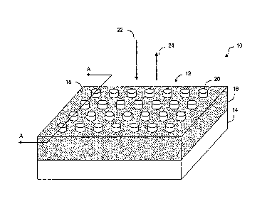
An exemplary embodiment of a wavelength selective surface 10 is shown in
FIG. 1. The wavelength selective surface 10 includes at least three
distinguishable layers.
The first layer is an electrically conductive outer or surface layer 12
including an
arrangement of surface elements 20. The surface elements 20 of the outer layer
12 are
disposed at a height above an inner layer including a continuous electrically
conductive
sheet, or wound layer 14. The arrangement of surface elements 20 and ground
layer 14 is
separated by an intermediate layer 16 disposed therebetween. At least one
function of the
intermediate layer 16 is to maintain a physical separation between the
arrangement of
= surface elements 20 and the ground layer 14. The intermediate layer 16
also provides
electrical isolation bemeen the two electrically conductive layers 12, 14.
In operation, wavelength selective surface 10 is exposed to incident
electromagnetic radiation 22. A variable portion of the incident radiation 22
is coupled to
the wavelength selective surface 10. The level of coupling depends at least in
part upon
the wavelength of the incident radiation 22 and a resonant wavelength of the
wavelength
zo selective surface 10, as determined by related design parameters.
Radiation coupled to
the wavelength selective surface 10 can also be referred to as absorbed
radiation. At
other non-resonant wavelengths, a substantial portion of the incident
radiation is reflected
24.
In more detail, the electrically conductive surface layer 12 includes multiple
discrete surface features, such as the electrically conductive surface
elements 20 arranged
in a pattern along a surface 18 of the intermediate layer 16. The discrete
nature of the
arrangement of surface features 20 requires that individual surface elements
20 are
isolated from each other. This also precludes interconnection of two or more
individual
surface elements 20 by electrically conducting paths. Two or more individual
surface
elements which are connected electrically form a composite surface element
which gives
rise to a new resonance.
-4-
CA 02637339 2008-06-12
WO 2007/149121 PCT/US2006/047449
The electrically conductive surface layer 12 including an arrangement of
surface
elements 20 is typically flat, having a smallest dimension, height, measured
perpendicular
to the intermediate layer surface 18. In general, each surface element 20
defines a surface
shape and a height or thickness measured perpendicular to the intermediate
layer surface
18. In general, the surface shape can be any closed shape, such as closed
curves, regular
polygons, irregular polygons, star-shapes having three or more legs, and other
closed
structures bounded by piecewise continuous surfaces including one or more
curves and
lines. In some embodiments, the surface shapes can include annular features,
such as ring
shaped patch with an open center region. More generally, the annular features
have an
outer perimeter defining the outer shape of the patch and an inner perimeter
defining the
shape of the open inner region of the patch. Each of the outer an inner
perimeters can .
have a similar shape, as in the ring structure, or a different shape. Shapes
of the inner and
outer perimeters can include any of the closed shapes listed above (e.g., a
round patch
with a square open center).
is The shapes can be selected to provide a resonant response having a
preferred
polarization. For example, surface features having an elongated shape provide
a resonant
response that is more pronounced in a polarization that is related to the
orientation of the
elongated shape. Thus, an array of vertically aligned narrow rectangles
produces a
response having a vertically aligned linear polarization. In general,
preferred
polarizations can be linear, elliptical, and circular.
Each of the electrically conductive surface elements 20 is formed with an
electrically conductive material. Such conductive materials include ordinary
metallic
conductors, such as aluminum, copper, gold, silver, iron, nickel, tin, lead,
and zinc; as
well as combinations of one or more metals in the form of a metallic alloy,
such as steel,
and ceramic conductors such as indium tin oxide and titanium nitride.
Alternatively or in
addition, conductive materials used in formation of the surface elements 20
include
semiconductors. Preferably, the semiconductors are electrically conductive.
Exemplary
semiconductor materials include: silicon and germanium; compound
semiconductors such
as silicon carbide, gallium-arsenide and indium-phosphide; and alloys such as
silicon-
germanium and aluminum-ga. llium-arsenide. 'Electrically conductive
semiconductors are
typically doped with one or more impurities in order to provide good
electrical
conductivity. Similarly, the ground layer 14 can include one or more
electrically
conductive materials, such as those described herein.
-5-
CA 02637339 2008-06-12
WO 2007/149121 PCT/US2006/047449
The intermediate layer 16 can be formed from an electrically insulative
material,
such as a dielectric providing electrical isolation between the arrangement of
surface
elements 20 and the ground layer 14. Some examples of dielectric materials
include
silicon dioxide (Si02); alumina (A1203); aluminum oxynitride; silicon nitride
(Si3N4).
Other exemplary dielectrics include polymers, rubbers, silicone rubbers,
cellulose
materials, ceramics, glass, and crystals. Dielectric materials also include:
semiconductors, such as silicon and germanium; compound semiconductors such as
silicon carbide, gallium-arsenide and indium-phosphide; and alloys such as
silicon-
germanium and alumfin-um-gallium-arsenide; and combinations thereof. As
dielectric
materials tend to concentrate an electric field within themselves, an
intermediate
dielectric layer 16 will do the same, concentrating an induced electric field
between each
of the surface elements 20 and a proximal region of the ground layer 14.
Beneficially,
such concentration of the electric-field tends to enhance electromagnetic
coupling of the
arrangement of surface elements 20 to the ground layer 14.
Dielectric materials can be characterized by parameters indicative of their
physical
properties, such as the real and imaginary portions of the index of
refraction, often
referred to as "n" and "k." Although constant values of these parameters n, k
can be used
to obtain an estimate of the material's performance, these parameters are
typically
wavelength dependent for physically realizable materials. In some embodiments,
the
intermediate layer 16 includes a so-called high-k material. Examples of such
materials
include oxides, which can have k values ranging from 0.001 up to 10_
The arrangement of surface elements 20 can be configured in a preferred
arrangement, or array on the intermediate layer surface 18. Referring now to
FIG. 2, the
wavelength selective surface 10 includes an exemplary array of flattened,
electrically
conductive surface elements 20. Multiple surface elements 20 are arranged in a
square
grid along the intermediate layer surface 18. A square grid or matrix
arrangement is an
example of a regular array, meaning that spacing between adjacent surface
elements 20 is
substantially uniform. Other examples of regular arrays or grids include
oblique grids,
centered rectangular grids, hexagonal grids, triangular grids, and Archimedean
grids. In
some embodiments, the grids can be irregular and even random. Each of the
individual
elements 20 can have substantially the same shape, such as the circular shape
shown.
Although flattened elements are shown and described, other shapes are
possible.
For example, each of the multiple surface elements 20 can have non-flat
profile with
-6-
CA 02637339 2008-06-12
WO 2007/149121 PCT/US2006/047449
respect to the intermediate layer surface 18, such as a parallelepiped, a
cube, a dome, a
pyramid, a trapezoid, or more generally any other shape. One major advantage
of the
present invention over other prior art surfaces is a relaxation of the
fabrication tolerances.
The high field region resides underneath each of the multiple surface elements
20,
between the surface element 20 and a corresponding region of the ground layer
14.
In more detailõ each of the circular elements 20 has a respective diameter D.
In
the exemplary square grid, each of the circular elements 20 is separated from
its four
immediately adjacent surface elements 20 by a uniform grid spacing A measured
center-
to-center. An alternative embodiinent of another wavelength selective surface
40
lo including a hexagonal arrangement, or array of surface elements 42 is
shown in FIG. 3.
Each of the discrete surface elements includes a square surface element 44
having a side
dimension D'. Center-to-center spacing between immediately adjacent elements
44 of' the
hexagonal array 42 is about A'. For operation in the infrared portion of the
electromagnetic spectrum, D will generally be between about-0.5 microns for
near
infrared and 50 microns for the far infrared and terahertz, understanding that
any such
limits are not firm and will very depending upon such factors as n, k, and the
thickness of
layers.
Array spacing A can be as small as desired, as long as the surface elements 20
do
not touch each other. Thus, a minimum spacing will depend to some extent on
the
dimensions of the suiface feature 20. Namely, the minimum spacing must be
greater than
the largest diameter of the surface elements (i.e., A > D). The surface
elements can be
separated as far as desired, although absorption response suffers from
increased grid
spacing as the fraction of the total surface covered by surface elements falls
below 10%.
An exemplary embodiment of an alternative family of wavelength selective
surfaces 30 is shown in FIG. 4. The alternative wavelength selective surfaces
30 also
include in intermediate layer 16 stacked above a ground layer 14; however, an
electrically
conductive surface 32 layer includes a complementary feature 34. The
complementary
feature 34 includes the electrically conductive layer 32 defining an
arrangement of
through apertures 36,, holes, or perforations.
The electrically conductive layer 32 is generally formed having a uniform
thickness. The arrangement of through apertures 34 includes multiple
individual through
apertures 36, each exposing a respective surface region 38 of the intermediate
layer 16.
Each of the through apertures 36 forms a respective shape bounded by a closed
perimeter
-7-
CA 02637339 2008-06-12
WO 2007/149121
PCT/US2006/047449
=
formed within the conductive layer 32. Shapes of each through aperture 36
include any
of the shapes described above in reference to the electrically conductive
surface elements
20 (FIG. 1), 44 (FIG. 3).
Additionally, the through apertures 36 can be arranged according to any of the
configurations described above in reference to the electrically conductive
surface
elements 20, 44. This includes a square grid, a rectangular grid, a triangular
grid, a
hexagonal grid, an oblique grid, a centered rectangular grid, and random
grids. Thus, any
of the possible arrangements of surface elements 36 and corresponding exposed
regions
of the intermediate layer surface 18 can be duplicated in a complementary
sense in that
lo the surface elements 20 are replaced by through apertures 36 and the
exposed regions of
the intermediate layer surface 18 are replaced by the electrically conductive
layer 32.
A cross-sectional elevation view of the wavelength selective surface 10 is
shown
in FIG. 5A. The electrically conductive ground layer 14 has a substantially
uniform
thickness HG. The intermediate layer 16 has a substantially uniform thickness
HD, and
each of the individual surface elements 20 has a substantially uniform
thickness Hp. The
different layers 12, 14, 16 can be stacked without gaps therebetween, such
that a total
thickness HT of the resulting wavelength selective surface 10 is substantially
equivalent to
the sum of the thicknesses of each of the three individual layers 14, 16, 12
(i.e., HT Ho
+ HD + Hp). A cross-sectional elevation view of the complementary wavelength
selective
surface 30 is shown in FIG. 5B and including a similar arrangement of the
three layers 14,
16, 32.
= In some embodiments, the intermediate insulating layer has a non-uniform
thickness with respect to the ground layer. For example, the intermediate
layer may have
a first thickness HD under each of the discrete conducting surface elements
and a different
thickness, or height at regions not covered by the surface elements. It is
important that a
sufficient layer of insulating material be provided under each of the surface
elements to
maintain a design separation and to provide isolation between the surface
elements and
the ground layer. In Lt least one example, the insulating material can be
substantially
removed at all regions except those immediately underneath the surface
elements. In
other embodiments, the insulating layer can include variations, such as a
taper between
surface elements. At least one benefit of the inventive design is a relaxation
of design
tolerances that results in a simplification of fabrication of the devices.
-8-
CA 02637339 2008-06-12
WO 2007/149121 PCT/US2006/047449
The thickness chosen for each of the respective layers 12, 32, 16, 14 (Hp, HD,
1-10)
can be independently varied for various embodiments of the wavelength
selective
surfaces 10, 30. For example, the ground plane 14 can be formed relatively
thick and
rigid to provide a support structure for the intermediate and surface layers
16, 12, 32.
Alternatively, the ground plane 14 can be formed as a thin layer, as long as a
thin ground
plane 14 forms a substantially continuous electrically conducting layer of
material
providing the continuous ground. Preferably, the ground plane 14 is at least
as thick as
one skin depth within the spectral region of interest. Similarly, in different
embodiments
of the wavelength selective surfaces 10, 30, the respective surface layer 12,
32 can be
io formed with a thickness Hp ranging from relatively thin to relatively
thick. In a relatively
thin embodiment, the surface layer thickness Hp can be a minimum thickness
required
just to render the intermediate layer surface 18 opaque. Preferably, the
surface layer 12,
32 is at least as thick as one skin depth within the spectral region of
interest.
Likewise, the intermediate layer thickness HD can be formed as thin as
desired, as
is long as electrical isolation is maintained between the outer and inner
electrically
conducting layers 12, 32, 14. The minimum thickness can also be determined to
prevent
electrical arcing between the isolated conducting layers under the highest
anticipated
induced electric fields. Alternatively, the intermediate layer thickness HD
can be formed
relatively thick. The concept of thickness can be defined relative to an
electromagnetic
20 wavelength 21/4, of operation, or resonance wavelength. For example, the
intermediate
layer thickness HD can be selected between about 0.01kc in a relatively thin
embodiment
to about 0.52we in a relatively thick embodiment.
The wavelength selective surfaces 10, 30 can he formed using standard
semiconductor fabrication techniques. Alternatively or in addition, the
wavelength
25 selective surfaces 10, 30 can be formed using thin film techniques
including vacuum
deposition, chemical vapor deposition, and sputtering. In some embodiments,
the
conductive surface layer 12, 44 can be formed using printing techniques. The
surface
features can be formed by providing a continuous electrically conductive
surface layer
and then removing regions of the surface layer to form the surface features.
Regions can
so be formed using standard physical or chemical etching techniques.
Alternatively or in
addition, the surface .features can be formed by laser ablation, removing
selected regions
of the conductive material from the surface, or by nano-imprinting or
stamping, or other
fabrication methods known to those skilled in the art.
-9-.
CA 02637339 2008-06-12
WO 2007/149121 PCT/US2006/047449
Referring to FAG_ 6A a cross-sectional elevation view of an alternative
embodiment of a wavelength selective surface 50.is shown having an over layer
52.
Similar to the embodiments described above, the wavelength selective surface
50 includes
an electrically conductive outer layer 12 having an arrangement of surface
elements 20
(FIG. 1) disposed at a height above a ground layer 14 and separated therefrom
by an
intermediate layer 16. The over layer 52 represents a fourth layer, or
superstrate 52
provided on top of the electrically conductive surface layer 12.
The over layer 52 can be formed having a thickness }lci measured from the
intermediate layer surface 18. In some embodiments, the over layer thickness 1-
Ici is
io greater than thickness of the surface elements 20 (i.e., Hci > Hp). The
over layer 52 can
be formed with varying thickness to provide a planar external surface.
Alternatively or in
addition, the over layer 52 can be formed with a uniform thickness, following
a contour
of the underlying electrically conductive surface 12.
An over layering material 52 can be chosen to have selected physical
properties
(e.g., k, n) that allow at least a portion of incident electromagnetic
radiation to penetrate
into the over layer 52 and react with one or more of the layers 12, 14, and 16
below. In
some embodiments, the overlying material 52 is optically transparent in the
vicinity of the
primary absorption wavelength, to pass substantially all of the incident
electromagnetic
radiation. For example, the overlying material 52 can be formed from a glass,
a ceramic,
a polymer, or a semiconductor. The overlaying material 52 can be applied using
any one
or more of the fabrication techniques described above in relation to the other
layers 12,
14, 16 in addition to painting and/or dipping.
In some embodiments, the over layer 52 provides a physical property chosen to
enhance performance of the wavelength selective device in an intended
application. For
example, the overlaying material 52 may have one or more optical properties,
such as
absorption, refraction, and reflection. These properties can be used to
advantageously
modify incident electromagnetic radiation. Such modifications include
focusing, de-
focusing, and filtering. Filters can include low-pass, high-pass, band pass,
and band stop.
The overlaying material 52 can be protective in nature allowing the wavelength
selective surface 50 to function, while providing environmental protection.
For example,
the overlaying material 52 can protect the surface conductive layer 12 from
corrosion and
oxidation due to exposure to moisture. Alternatively or in addition, the
overlaying
material 52 can protect either of the exposed layers 12, 16 from erosion due
to a harsh
-10-
CA 02637339 2008-06-12
WO 2007/149121 PCT/US2006/047449
(e.g., caustic) environment. Such harsh environments might be encountered
routinely
when the wavelength selective surface is used in certain applications. At
least one such
application that would benefit from a protective overlaying material 52 would
be a marine
application, in which a protective over layer 52 would protect the
electrically conductive
layer 12 or 32 from corrosion.
In another embodiment shown in FIG. 6B, a wavelength selective surface 60
includes an overlying material 62 applied over a conductive layer 32 defining
an
arrangement of through apertures 34 (FIG. 4). The overlying material 62 can be
applied
with a maximum thickness lic2 measured from the intermediate layer surface 18
to be
io greater than the thickness of the conductive layer 32 (i.e., lic2 > Hp).
The overlaying
material 62 again can provide a planar external surface or a contour surface.
Accordingly, a wavelength selective surface 60 having apertures 36 defined in
an
electrically conductive layer 32 is covered by an overlying material 62. The
performance
and benefits of such a device are similar to those described above in relation
to FIG. 6A.
Referring to FIG. 7A, an exemplary reflectivity versus wavelength response
curve
70 of a representative narrow-resonance response is shown in graphical form.
The
response curve 70 is achieved by exposing a wavelength selective surface 10
(FIG. 1)
constructed in accordance with the principles of the present invention to
incident
electromagnetic radiation 22 (FIG. 1) within a band including a resonance. As
shown, the
zo reflectivity to incident electromagnetic radiation varies according to
the curve 70 within'
the range of 0% to 100%. As the wavelength of the incident radiation 22 is
varied from 2
to 20 microns, the reflectivity starts at a relatively high value of about
75%, increases to a
value of over 85% at about 3 microns, reduces back to about 75% at about 3.5
microns,
and increases again to nearly 100% between about 3.5 and 7 microns. Between 7
and 8
microns, the reflectivity response curve 70 incurs a second and more
pronounced dip 72
to less then 20% reflectivity. The second dip 72 is steep and narrow,
corresponding to
absorption of incident electromagnetic radiation by the surface 10. The
reflectivity
response curve 70 at wavelengths beyond about 8 microns rises sharply back to
more than
90% and remains above about 80% out to at least 20 microns. This range, from 2
to 20
microns, represents a portion of the electromagnetic spectrum including
infrared
radiation.
The second and much more pronounced dip 72 corresponds to a primary
resonance of the underlying wavelength selective surface 10. As a result of
this
-11-
=
CA 02637339 2008-06-12
WO 2007/149121 PCT/US2006/047449
resonance, a substantial portion of the incident electromagnetic energy 22 is
absorbed by
the wavelength selecti.ve surface 10. A measure of the spectral width of the
resonance
response 70 can be determined as a width in terms of wavelength normalized to
the
resonant wavelength (i.e., Ak/kc or d%/X.c). Preferably, this width is
determined at full-
width-half-maximum (FWHM). For the exemplary curve, the width of the
absorption
band at FWHM is less than about 0.2 microns with an associated resonance
frequency of
about 7 microns. This results in a spectral width, or dX/X,e of about 0.03.
Generally, a
diAc value of less than about 0.1 can be referred to as narrowband. Thus, the
exemplary
resonance is representative of a narrowband absorption response.
Results supported by both computational analysis of modeled structures and
measurements suggest that the resonant wavelength associated with the primary
resonance response 72 is sensitive to a maximum dimension of the electrically
conductive
surface elements (e.g., a diameter of a circular patch D, or a side length of
a square patch
D'). As the diameter of the surface elements is increased, the wavelength of
the primary
'15 absorption band 72 also increases. Conversely, as the diameter of the
surface elements is
decreased, the wavelength of the primary absorption band 72 also decreases.
The first, less pronounced dip 74 in reflectivity corresponds to a secondary
absorption band of the underlying wavelength selective surface 10. Results
supported by
both computational analysis of modeled structures and measurements suggest
that the
wavelength associated with the secondary absorption band 74 corresponds at
least in part
to a center-to-center spacing of the multiple electrically conductive surface
elements. As
the spacing between surface elements 20 in the arrangement of surface elements
20 is
reduced, the wavelength of the secondary absorption band 74 decreases.
Conversely, as
the spacing between the arrangement of surface elements 20 is increased, the
wavelength
of the secondary absorption band 74 increases. The secondary absorption band
74 is
typically less pronounced than the primary absorption band 72, such that a
change in
reflectivity AR can be determined between the two absorption bands 74, 72. A
difference
in wavelength between the primary and secondary absorption bands 72, 74 is
shown as
AW.
In general, the performance may be scaled to different wavelengths according
to
the desired wavelength range of operation. Thus, by scaling the design
parameters of any
of the wavelength selective surfaces as described herein, resonant performance
can be
obtained within any desired region of the electromagnetic spectrum. Resonant
-12-
CA 02637339 2008-06-12
WO 2007/149121 PCT/US2006/047449
wavelengths can range down to visible light and even beyond into the
ultraviolet and X-
ray. At the other end of the spectrum, the resonant wavelengths can range into
the
terahertz band (e.g., wavelengths between about 1 millimeter and 100 microns)
and even
up to radio frequency bands (e.g., wavelengths on the order of centimeters to
meters).
Operation at the shortest wavelengths will be limited by available fabrication
techniques.
Current techniques can easily achieve surface feature dimensions to the sub-
micron level.
It is conceivable that such surface features could be provided at the
molecular level using
currently available and emerging nanotechnologies. Examples of such techniques
are
readily found within the field of micro-mechanical-electrical systems (MEMS).
Referring to FIG. 7B, an exemplary reflectivity versus wavelength response
curve
80 of a wide-resonance wavelength selective surface is shown in graphical
form. This
wideband response curve 80 can also be achieved with the wavelength selective
surface
10 (FIG. 1) constructed in accordance with the principles of the present
invention, but
having a different selection of design parameters. Here, a primary absorption
band 82
occurs at about 8 microns, with wavelength range at FWHM of about 3 microns.
This
results in a spectral width Ak/kc of about 0.4. A spectral width value AM,
greater than
0.1 can be referred to as broadband. Thus, the underlying wavelength selective
surface
10 can also be referred to as a broadband structure.
One or more of the physical parameters of the wavelength selective surface 10
can
be varied to control reflectivity response of a given wavelength selective
surface. For
example, the thickness of one or more layers (e.g., surface element thickness
Hp,
dielectric layer thickness HD, and over layer thickness HO can be varied.
Alternatively or
in addition, one or more of the materials of each of the different layers can
be varied. For
example, the dielectric material can be substituted with another dielectric
material having
a different n and k values. The presence or absence of an over layer 52 (FIG.
6A), as well
as the particular material selected for the over layer 52 can also be used to
vary the
reflectivity or absorption response of the wavelength selective surface.
Similar
performance changes may be achieved by changing the material of the ground
plane,
change the dimension D of the surface elements, or by changing the shape of
the surface
elements.
In a first example, a wavelength selective surface includes an intermediate
layer
formed with various diameters of surface patches. The wavelength selective
surface
includes a triangular array of round aluminum patches placed over an aluminum
film
-13-
CA 02637339 2008-06-12
WO 2007/149121 PCT/US2006/047449
ground layer. The various surfaces are each formed with surface patches having
a
different respective diameter. A summary of results obtained for the different
patch
diameters is included in Table 1. In each of these exemplary embodiments, the
patch
spacing between adjacent patch elements was about 3.4 microns, and the
thickness or
depth of the individual patches and of the ground layer film were each about
0.1 micron.
An intermediate, dielectric layer having thickness of about 0.2 microns was
included
between the two aluminum layers. It is worth noting that the overall thickness
of the
wavelength selective surface is about 0.4 microns ¨ a very thin material. The
exemplary
dielectric has an index of refraction of about 3.4. Table 1 includes
wavelength values
io associated with the resulting primary absorptions. As shown, the
resonant wavelength
increases with increasing patch size.
Table 1. Primary Absorption Wavelength Versus Patch Diameter
Patch Diameter Resonant Wavelength (XG)
1.25 lam 4.1 pm
1.75 pm 5.5 pm
2.38 pm 7.5 pm
2.98 pm 9.5 gm
In another example, triangular arrays of circular patches having a uniform
array
spacing of 3.4 microns and patch diameter of 1.7 microns are used. A
dielectric material
provided between the outer conducting layers is varied. As a result, the
wavelength of the
primary absorption shifts. Results are included in Table 2.
Table 2. Resonance Versus Dielectric Material
¨Dielectric material Resonant Wavelength (1t.c)
Oxide 5.8 jArn
Nitride 6.8 lam
Silicon 7.8 pm
While this invention has been particularly shown and described with references
to
preferred embodiments thereof, it will be understood by those skilled in the
art that
various changes in form and details may be made therein without departing from
the
scope of the invention encompassed by the appended claims.
-14-