Note: Descriptions are shown in the official language in which they were submitted.
CA 02637467 2008-07-17
WO 2007/094971 PCT/US2007/002655
-1-
ELECTRONIC BALLAST HAVING ADA.PTIVE FREQUENCY SHIFTING
CROSS REFERENCE TO RELATED APPLICATIONS
[0001] This patent application is based on and claims priority to U.S. Patent
Application, Serial No. 11/352,962, filed February 13, 2006 and entitled
ELECTRONIC
BALLAST HAVING ADAPTIVE FREQUENCY SHIFTING, the contents of which are
incorporated by reference as if set forth fully herein.
FIELD OF THE INVENTION
[0002] The present invention relates to electronic ballasts and, more
particularly, to
electronic dimming ballasts for gas discharge lamps, such as fluorescent
lamps.
BACKGROUND OF THE INVENTION
[0003] Electronic ballasts for fluorescent lamps typically can be analyzed as
comprising a "front-end" and a "back-end". The front-end typically includes a
rectifier for
changing alternating-current (AC) mains line voltage to a direct-current (DC)
bus voltage,
and a filter circuit, e.g., a capacitor, for filtering the DC bus voltage. The
front-end of
electronic ballasts also often includes a boost converter, which is an active
circuit for
boosting the magnitude of the DC bus voltage above the peak of the line
voltage and for
improving the total harmonic distortion (THD) and the power factor of the
input current to
the ballast. The ballast back-end typically includes a switching inverter for
converting the
DC bus voltage to a high-frequency AC voltage, and a resonant tank circuit
having a
relatively high output impedance for coupling the high-frequency AC voltage to
the lamp
electrodes.
CA 02637467 2008-07-17
WO 2007/094971 PCT/US2007/002655
-2-
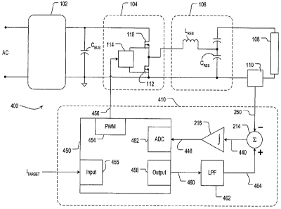
[00041 Referring first to Fig. 1, there is shown a simplified block diagram of
a prior
art electronic ballast 100. The ballast 100 includes a front-end 102 for
producing a
substantially DC bus voltage across a bus capacitor, CBUs, from an AC input
voltage. The
ballast 100 further comprises an inverter 104 for converting the DC bus
voltage into a
high-frequency voltage for driving a lamp current in a fluorescent lamp 108.
The
high-frequency voltage provided by the inverter 104 is coupled to the lamp 108
through a
resonant tank 106 having a resonant inductor, LREs, and a resonant capacitor,
C.
[0005] The inverter 104 includes first and second series-connected switching
devices
112, 114 and a gate drive circuit 116. The switching devices 112, 114 in the
inverter 104 are
controlled using a d(1-d) complementary switching scheme. In the d(1-d)
complementary
switching scheme, the first switching device 112 has a duty cycle of d and the
second
switching device 114 has a duty cycle of 1-d_ The switching devices 112, 114
are controlled
by the gate drive circuit 116 such that only one switching device is
conducting at a time.
When the first switching device 112 is conducting, then the output of the
inverter 104 is
pulled upwardly toward the DC bus voltage. When the second switching device
114 is
conducting, then the output of the inverter 104 is pulled downwardly toward
circuit common.
[0006] The current through the lamp 108 is controlled by changing the
frequency
andlor the duty cycle of the high-frequency voltage at the output of the
inverter 104. A
current sense circuit 110 is coupled in series with the lamp 108 and provides
a larnp current
signal 250 representative of the magnitude of the current through the lamp. An
analog
control circuit 210 is responsible for controlling the gate drive circuit 116
and thus the
switching devices 112, 114 of the inverter 104. The analog control circuit 210
includes a
reference circuit 212, a summing circuit 214, a compensator circuit 216, a
frequency-shift
circuit 218, a triangle-wave oscillator 222, and a comparator 220. The
reference circuit 212
provides a reference signal 242 representative of a target current I-i-AizcET
for the lamp 108.
The summing circuit 214 receives the lamp current signal 250 and the reference
signal 242
and creates an error signal 240 representative of the difference between the
target current and
the actual current in the lamp 108. The compensator circuit 216 receives the
error signal 240
and provides a duty cycle request voltage 246 that is proportional to the
desired duty cycle of
the inverter 104.
CA 02637467 2008-07-17
WO 2007/094971 PCT/US2007/002655
-3-
[00071 The frequency shift circuit 218 also receives the reference signal 242
and
provides a desired frequency signal 245 representative of the desired inverter
frequency. The
triangle-wave oscillator 222 receives the desired frequency signal 245 from
the fi-equency
shift circuit 218 and provides a triangle-wave signal 244 at the desired
frequency. The
comparator 220 receives both the triangle wave signal 244 and the duty cycle
req'uest voltage
246 and produces a pulse width modulated (PWM) signal 248 with the desired fi-
equency and
duty cycle. This PWM signal 248 is provided to the gate drive circuit 116,
wliich drives the
switches 112, 114 in the inverter 104.
[0008] In addition to the normal running mode, the ballast 100 has several
other
modes of operation including a "preheat" mode and a "strike" mode. The purpose
of the
preheat mode is to heat the lamp filaments prior to the application of a
sufficient voltage to
strike the lamp. During the strike mode, the lamp voltage is increased until
either the lamp
strikes or a predetermined voltage limit is reached.
[0009] Preheat is accomplished by controlling the frequency of the inverter
104 to a
preheat frequency, which is greater than the frequency of the inverter 104 in
norn-ial
operation. During preheat, the compensator circuit 216 is always in control of
the duty cycle
of the inverter 104. At the same time, the reference circuit 212 provides a
reference signal
242 at a level that represents a non-zero lamp current. Since there is no
current through the
lamp during preheat, the current sense circuit 110 produces the lamp current
signal 250 with a
positive magnitude and thus the output of the summing circuit 214, i.e., the
error signal 240,
has a non-zero value. The compensator circuit 216 includes an integrator (not
shown), so the
non-zero error signa1240 causes the compensator circuit 216 to increase the
duty cycle of the
duty cycle request voltage 246 to 50%, at which time the compensator circuit
saturates. At
this point, the duty cycle of the duty cycle request voltage 246 is fixed at
50% and the preheat
voltage is adjusted by changing the frequency. It is important to note that
since the
compensator circuit 216 contains an integrator, it is not possible to set the
duty cycle to an
arbitrary level. In practice, the choices would be saturated at 50% or
saturated at 0%. An
alternative would be to provide additional circuitry to clamp the output of
the compensator
circuit 216 at a given level during preheat, but this would add additional
cost and complexity.
CA 02637467 2008-07-17
WO 2007/094971 PCT/US2007/002655
-4-
[0010] To strike the lamp 108, i.e., in the strike mode, the operating
frequency of the
inverter 104 is swept down from the preheat frequency to a low-end frequency.
Preferably,
the low-end frequency is near the resonant frequency wR of the resonant tank
106, i.e.,
wR = 1/4(LRES * CRES). Accordingly, the voltage at the output of the resonant
tank 106 at the
low-end frequency is substantially large and is appropriate to strike the lamp
108, When the
lamp 108 strikes, the lamp current begins to flow through the lamp. At this
time, the
compensator circuit 216 of the analog control circuit 210 is still saturated
and the duty cycle
of the duty cycle request voltage 246 is still 50%. As a result, a current
above the target
current starts to flow through the lamp 108. This excess current will cause
the compensator
circuit 216 to come out of saturation and to set the duty cycle of the PWM
signal 248 so as to
maintain the target current in the lamp 108. While the compensator circuit 216
is saturated,
the current in the lamp 108 can be significantly higher than the target
current. The lligh
current, along with the time required for the loop to come out of saturation,
can result in a
noticeable flash when the lamps strike.
[0011] A simplified schematic diagram of another prior art electronic ballast
300 is
shown in Fig. 2. The ballast 200 operates in a similar manner as the ballast
100 shown in Fig.
1, but the analog control circuit 210 has been replaced by a digital control
circuit 310. An
analog-to-digital converter (ADC) 352 in a microprocessor 350 receives the
lamp current
signa1250 from the current sense circuit I 10 and converts it into an 8-bit
digital
representation. The reference signal 242 representative of the target current
in the lamp 108
is received at an input 355. The software in the microprocessor 350 then
compares the
measured current with the target current to generate an error signal, which is
then used to
generate a desired duty cycle. The desired frequency is determined from the
desired current.
A pulse-width modulated (PWM) signal 356 is produced at an output 354 of the
microprocessor 350. The software in the microprocessor 350 drives the PWM
signal 356
with the desired frequency and duty cycle and provides the PWM signal to the
gate drive
circuit 116. In the ballast 300, software in the microprocessor 350 of the
digital control
circuit 310 provides the functionality that was provided by the analog control
circuit 210 of
the ballast 100.
[0012] The digital implementation of the preheat mode of the ballast 300 is
very
different than the preheat mode of the ballast 100. The software that normally
implements
CA 02637467 2008-07-17
WO 2007/094971 PCT/US2007/002655
-5-
the conlpensator routine is not in control of the inverter duty cycle. In
fact, a cornpletely
different routine is in control of the inverter. As a result, it is possible
to directly control both
the duty cycle and the frequency to achieve the desired preheat level.
[0013] In the digital implementation of the strike mode, the duty cycle is
held at a
fixed level and the frequency is swept down from the preheat frequency to the
low-end
frequency. During this period, the software must monitor the lamp voltage and
lamp current
to detect when the lamp strikes. It is very important to detect when the lamp
strikes because
once it is struck, a different routine must be run to implement the normal
operation control
loop. Since both the frequency and duty cycle are controllable during strike,
it would be
possible to set the duty cycle to something less than 50% during the strike
phase. The lower
duty cycle would result in the lamp starting at a lower current to help reduce
flasli. However,
in order to ensure accurate detection of lamp strike, the lamp must strike
with a relatively
high current.
[0014] Replacing the analog control circuit 210 of the ballast 100 with the
digital
control circuit 310 of the ballast 300 has several benefits. First, there are
fewer parts in the
digital control circuit 310 since most of the control functions are completed
by the
microprocessor 350. Second, the control functions provided by the
microprocessor 350 can
be easily altered without the need to change any hardware of the digital
control circuit 310.
Further, situation-specific software can be executed when the ballast 300 is
in different
normal and abnormal modes of operation.
[0015] However, the digital control circuit 310 has some disadvantages in view
of the
analog control circuit 210. The capability of the microprocessor 350 is
dependent on the cost
of the device. So, in order to achieve a reasonable cost, some compromises may
need to be
made in the areas of core speed, ADC resolution, ADC sampling rate and math
capability.
Quantization effects of the ADC conversion can become significant at low dim
levels. This
can be improved with a higher resolution ADC or a higher sampling rate, but as
mentioned
earlier, higher capability results in higher cost for the microprocessor 350.
[0016] Both the analog control circuit 210 and the digital control circuit 310
of the
prior art ballast 100, 300 use an open-loop frequency shift in which there is
a predetermined
CA 02637467 2008-07-17
WO 2007/094971 PCT/US2007/002655
-6-
operating frequency for a given desired light level. The concept of adjusting
botli the
frequency and the duty cycle of the inverter 104 is described in greater
detail in U.S. Patent
No. 6,452,344, issued September 17, 2002, entitled "Electronic Dimming
Ballast", which is
hereby incorporated herein by reference in its entirety.
[00171 Fig. 3 is a simple control system diagram illustrating the control
loops of the
prior art ballasts 100, 300. The operating duty cycle, dop, of the inverter is
controlled through
a closed-loop technique, while the operating frequency, foP, is controlled
through an open-
loop technique. The actual lamp current, IACTUAL, is provided as feedback to
the duty-cycle
control loop and is subtracted from the target current, ITARGET, to produce a
lamp current error
signal, eI, and ultimately, the desired operating duty cycle doP. In contrast,
the desired
operating frequency fop is simply generated solely in response to the target
current ITAxGET.
[0018] Fig. 4 shows a plot of the target operating frequency of the inverter
104 versus
the lainp current and a plot of the operating frequency versus the lamp
current at a fixed 50%
duty cycle, which demonstrates the maximum current that can be delivered by
the ballast 100,
300 at a given frequency. At low light levels, the ballast operating frequency
is maintained at
the low-end frequency fLOw_END, which is near the resonant frequency of the
resonant tank
106. Above a predetermined level, the operating frequency is decreased
linearly as the lamp
current increases, i.e., as the desired lighting level of the lamp 108
increases towards high-
end.
[0019] One complication that results from operating the inverter 104 at
a.frequency
that is away from the resonant frequency when utilizing the d(1-d) switching
scheme (i.e., at
high-end) is the possibility of "mercury pumping". As the operating frequency
moves away
from the resonant frequency, and the impedance of the lamp 108 decreases (as
the lamp
current increases), the filtering effect of the resonant tank 106 is reduced.
When the inverter
104 is operating at any duty cycle other than 50%, the voltage at the output
of the inverter is
asymmetric and contains second harmonic content. For duty cycles near 50%, the
second
harmonic is not significant. However, as the duty cycle moves away from 50%,
the second
harmonic content increases.
CA 02637467 2008-07-17
WO 2007/094971 PCT/US2007/002655
-7-
[0020] When operating at the high-end frequency fHiow_ENO, a significant
amount of
this second harmonic content from the inverter 104 is passed through the
resonant tank 106 to
the lamp 108. As a result, the lamp current is not symmetric. Blocking
capacitors, e.g.,
capacitor 118 in Figs. I and 2, at the output of the ballast 100, 300 prevent
the ballast from
delivering significant DC current to the lamp 108. However, the asymmetric
current in the
lamp 108 coupled with the non-linear lamp load results in a DC voltage on the
lamp 108.
The DC voltage on the lamp 108 will cause mercury ions to migrate from one end
of the lamp
to the other. If the DC voltage is high enough, the lamp 108 will become
starved for mercury
at one end. As a result, the starved end of the lamp 108 will produce less
light and may also
turn pink.
[0021] In order to avoid significant mercury pumping, the analog control
circuit 210
and the digital control circuit 310 of the prior art ballasts 100, 300
utilized frequency shift
profiles that were selected to insure that the duty cycle was as close to 50%
as possible when
operating at the high-end frequency. However, the tolerances of the components
of the
resonant tank 106, and the variations in the operating characteristics of
common fluorescent
lamps, require that the frequency be selected such that even worst-case
combinations are
capable of reaching the needed high-end current IxICH_END. The constraints of
being able to
reach high-end in the worst case while having the highest duty cycle possible
result in the
need for tight tolerances on components and the need to tailor tank component
values to a
narrow load range.
[0022] Thus, there exists a need for an electronic ballast that avoids mercury
pumping
and operates at high-end with a duty cycle close to 50% and has a broad range
of load types,
but does not require a resonant tank that has components with small
tolerances.
SUMMARY OF THE INVENTION
[0023] According to the present invention, an electronic ballast for driving a
gas
discharge lamp includes an inverter, a resonant tank, a control circuit, and a
current sense
circuit. The inverter converts a substantially DC bus voltage to a high-
frequency AC voltage
having an operating frequency and an operating duty cycle. The resonant tank
couples the
high-frequency AC voltage to the lamp to generate a present lamp current
through the lamp.
CA 02637467 2008-07-17
WO 2007/094971 PCT/US2007/002655
-8-
The control circuit is operable to control the operating frequency and the
operating duty cycle
of the high-frequency AC voltage of the inverter. The current sense circuit
provides to the
control circuit a present lamp current signal representative of the present
lamp current. The
control circuit is operable to control the operating duty cycle of the high-
frequency AC
voltage of the inverter in response to a target lamp current signal and the
present lamp current
signal. Further, the control circuit is operable to control the operating
frequency of the high-
frequency AC voltage of the inverter in response to the operating duty cycle
and a target duty
cycle, such that the control circuit is operable to minimize the difference
between the
operating duty cycle and the target duty cycle. Preferably, the control
circuit is further
operable to control the operating frequency to a base operating frequency in
dependence on
the target lamp current signal, when the target lamp current changes in value.
[00241 The present invention further provides a method for controlling an
electronic
ballast for driving a gas discharge lamp. The ballast comprises an inverter
characterized by
an operating frequency and an operating duty cycle. The method comprises the
steps of
generating a present lamp current through the gas discharge lamp in response
to the operating
frequency and the operating duty cycle of the inverter; generating a present
Iamp current
signal representative of the present lamp current; receiving a target lamp
current signal
representative of a target lamp current; controlling the duty cycle of the
inverter in response
to the target lamp current signal and the present lamp current signal; and
controlling the
operating frequency of the inverter in response to the target lamp current
signal, the operating
duty cycle of the inverter, and a target duty cycle, such that the difference
between the
operating duty cycle and the target duty cycle is minimized.
[0025] In addition, the present invention provides a control circuit for an
electronic
ballast having an inverter for driving a gas discharge lamp. The control
circuit is operable to
control an operating frequency and an operating duty cycle of the inverter of
the ballast. The
control circuit comprises a duty cycle control portion for controlling the
operating duty cycle
of the inverter in response to a target lamp current signal and a present lamp
current signal,
and a frequency control portion for controlling the operating frequency of the
inverter in
response to the target lamp current signal, the operating duty cycle, and a
target duty cycle.
The difference between the operating duty cycle and the target duty cycle is
minimized.
CA 02637467 2008-07-17
WO 2007/094971 PCT/US2007/002655
-9-
BRIEF DESCRIPTION OF THE DRAWINGS
[0026] Fig. 1 is a simplified schematic diagram of a prior art electronic
ballast having
an analog control circuit;
[0027] Fig. 2 is a simplified schematic diagram of a prior art electronic
ballast having
a digital control circuit;
[0028] Fig. 3 is a simplified control system diagram illustrating the control
loops of
the prior art ballasts of Figs. 1 and 2;
[0029] Fig. 4 is a plot of the operating frequency of an inverter of the
electronic
ballast of Figs. 1 and 2 versus the lamp current;
[0030] Fig. 5A is a simplified schematic diagram of an electronic ballast
according to
the present invention;
[0031] Fig. 5B is a simplified schematic diagram of the electronic ballast of
Fig. 5A;
[0032] Figs. 6A and 6B are flowcharts of the software executed by a
microprocessor
of the ballast of Fig. 5A according to the present invention;
[0033] Fig. 6C is a flowchart of the software executed by the microprocessor
of the
ballast of Fig. 5A in response to a change in a target lamp current;
[0034] Fig. 7 shows a plot of the operating frequency of the electronic
ballast of Fig.
5A according to the present invention;
[0035] Fig. 8 is a control system diagram illustrating the control loops of
the ballast
according to a first embodiment of the present invention of Fig. 5A;
[0036] Fig. 9 is a control system diagram illustrating the control loops of a
second
embodiment of the ballast of the present invention;
[0037] Fig. 10 is a flowchart of the software executed by a microprocessor of
the
ballast of Fig. 9 according to a second embodiment of the present invention;
and
CA 02637467 2008-07-17
WO 2007/094971 PCT/US2007/002655
-10-
[0038] Fig. 11 is a simplified schematic diagram of a ballast according to a
third
embodiment of the present invention.
DETAILED DESCRTPTION OF THE INVENTION
[0039] The foregoing summary, as well as the following detailed description of
the
preferred embodiments, is better understood when read in conjunction with the
appended
drawings. For the purposes of illustrating the invention, there is shown in
the drawings an
embodiment that is presently preferred, in which like numerals represent
siinilar pai-ts
throughout the several views of the drawings, it being understood, however,
that the
invention is not limited to the specific methods and instrumentalities
disclosed.
[0040] Fig. 5A shows a simplified block diagram of an electronic ballast 400
according to the present invention. The ballast 400 includes many similar
blocks as the prior
art ballasts 100, 300, which each have the same function as described
previously. However,
those components of the ballast 300 that differ from the prior art ballast 100
will be described
in greater detail below.
[0041] The ballast 400 includes a hybrid analog/digital control circuit 410.
The
hybrid control circuit 410 improves on the characteristics of the analog
control circuit 210
and digital control circuit 310 of the prior art ballasts 100, 300. The hybrid
control circuit
410 includes the summing circuit 214 and the compensator circuit 216, which
function the
same as those circuits in the prior art ballast 100.
[0042] The hybrid control circuit 410 further comprises a microprocessor 450,
which
provides a PWM signa1456 at an operating frequency, fop, and an operating duty
cycle, doP,
to the gate drive circuit 116 of the inverter 104. The microprocessor 450
receives a target
lamp current, ITARGET, via an input 455. The target lamp current ITaRGET may
be obtained, for
example, from a phase-control input (not shown) or from a digital message
received from a
communication link (not shown). A ballast operable to receive a phase-control
input is
described in greater detail in the previously mentioned U.S. Patent No.
6,452,344. A ballast
operable to be coupled to a digital communication link is described in greater
detail in co-
pending U.S. Patent Application Serial No. 10/824,248, Publication No.
2005/0179404, filed
CA 02637467 2008-07-17
WO 2007/094971 PCT/US2007/002655
-11-
April 14, 2004, entitled "Multiple-Input Electronic Ballast with Processor",
which is hereby
incorporated herein by reference in its entirety.
[0043] The microprocessor 450 provides a PWM reference signal 460, having a
duty
cycle dependent on the target lamp current ITARGET, at an output port 458. A
low pass filter
462 generates a DC reference signal 464, which is representative of a desired
current in the
lamp 108, from the PWM reference signal 460. The summing circuit 214 receives
the
present lamp current signal 250 and the DC reference signal 464 and creates a
lamp current
error signal 440 representative of the difference between the target current
and the actual
current in the lamp. The compensator circuit 216 receives the error signal 440
and provides a
duty cycle request signal 446, which is a DC voltage inversely proportional to
the desired
duty cycle of the inverter 104.
[0044] Fig. 5B is a simplified schematic diagram of the electronic ballast 400
showing the current sense circuit 110 and the hybrid control circuit 410 in
greater detail.
During the negative portions of the AC current through the lamp 108, the lamp
current flows
through a resistor R570 and a diode D572. Alternatively, the lamp current
flows through
only a diode D574 to circuit common during the positive portions of the lamp
current. A
resistor R576 and a capacitor C578 filter the voltage produced across the
resistor R570 and
generate the lamp current signal 250. Accordingly, the lainp current signal
250 provides a
substantially DC voltage having a negative magnitude representative of the
current through
the lamp 108.
(0045] The PWM reference signal 460 provided at the output port 458 of the
microprocessor 450 is filtered by the low pass filter 462 comprising a
resistor R580 and a
capacitor C582 to produce the DC reference signal 464 representative of the
target lamp
current ITARGET. The DC reference signal 464 and the lamp current signal 250
are provided to
the inverting input of an operational amplifier (op amp) 584 through resistors
R586 and
R588, respectively. A DC offset voltage VOFFSET is provided to the non-
inverting input of the
op amp 584. A capacitor C590 is connected between the inverting input and the
output of the
op amp 584 to provide the integration functionality of the compensator circuit
216.
Accordingly, the output of the op amp 584 is a function of the integral of the
sum of the DC
reference signal 464 and the lamp current signal 250. Finally, the voltage at
the output of the
CA 02637467 2008-07-17
WO 2007/094971 PCT/US2007/002655
-12-
op amp 584 is filtered by a resistor R592 and a capacitor C594 to provide the
duty cycle
request signal 446 to the microprocessor 450.
[0046] Figs. 6A and 6B are flowcharts of the software executed cyclically by
the
microprocessor 450 of the ballast 400 in order to adaptively change the
operating frequency
foP of the inverter 104 according to the present invention. The flowcharts of
Figs. 6A and 6B
will be described with reference to the schematic diagram of the ballast 400
of Fig. 5A.
Preferably, the process of Figs. 6A and 6B repeats every 104 sec.
[0047] An ADC 452 in the microprocessor 450 receives the duty cycle request
signal
446 and converts the signal into a digital value (at step 502). Since the duty
cycle request
signal 446 is inversely proportional to the operating duty cycle doP, the
microprocessor 450
inverts and scales the digital value to generate the operating duty cycle doP.
For example, the
operating duty cycle doP is linearly scaled such that a digital value of 0
corresponds to an
operating duty cycle of 0% and a digital value of 512 corresponds to an
operating duty cycle
of 100%. In normal operation, the software in the microprocessor 450 uses the
operating
duty cycle doP along with the operating frequency foP to calculate an
operating period, ToP,
and an on-time, tON. The operating frequency fop is detennined from the target
lamp current
ITARGET and the operating duty cycle doP, as will be described in greater
detail below. The '
operating period ToP and the on-time tON are used by a PWM module 454 to
provide the
PWM signal 456 at the operating frequency foP and the operating duty cycle
doP. The
microprocessor 450 is operable to set the operating duty cycle doP as either
the duty cycle
provided by the duty cycle request signa1446 or some other duty cycle.
[0048] While in normal operation, the microprocessor 450 monitors the present
operating duty cycle doP of the inverter 104. The operating duty cycle doP is
subtracted from
a predetermined target duty cycle, dTARGET, e.g., preferably 43%, to obtain a
duty cycle error
value, ed (at step 504). If the error value ed is inside of a dead-band (at
step 506), the process
loops around to read the duty cycle request signal 446 again. The dead-band is
a range,
through which the error value ed can be varied without initiating a response
in order to
prevent oscillations. The dead-band is preferably 1% above and below the
predetermined
target duty cycle dTARGET, e.g., 42% to 44%. If the duty cycle error value ed
is outside of the
dead-band, the error value is then limited to a maximum positive error value,
eMAx+, e.g., 2%,
CA 02637467 2008-07-17
WO 2007/094971 PCT/US2007/002655
- 13-
or a maximum negative error value, eMAx_,e.g., -2%, (at step 510) in
dependence on the sign
of the error value. For example, if the error value ed is -2.5%, the error
value ed will be
limited to -2%.
[0049] Next, the error value ed is added to a 16-bit accumulator ACC in the
microprocessor 450, thereby increasing (or decreasing) the value of the
accumulator (at step
512). When the accumulator reaches a predetermined positive value (or a
predetermined
negative value), the microprocessor 450 will reset the accumulator and change
the operating
frequency foP of the ballast (as described in greater detail below).
Accordingly, if the error
value ed is large, the accumulator will reach the predetermined positive (or
negative) value
more quickly. Preferably, the predetermined positive and negative values
correspond to the
size of the accumulator, e.g., +(216 - 1) and -(216 - 1), respectively, for
the 16-bit
accumulator ACC. The accumulator reaches the predetermined positive value (or
the
predetermined negative value) when the accumulator overflows. The
microprocessor 450 acts
on the overflow of the accumulator by reading a carry flag (which is set when
the
accumulator overflows) and a negative flag (which is set when the accumulator
lias a
negative value). When the accumulator overflows, the value of the accumulator
is
automatically reset to zero. The accumulator is also reset to zero at the
startup of the
microprocessor 450.
[0050] Referring to Fig. 6B, if the duty cycle is above (or below) the
predetermined
target duty cycle dTARGET, the microprocessor 450 will slowly decrease (or
increase) the
operating frequency foP of the inverter 104, thereby decreasing (or
increasing) the required
duty cycle doP to deliver the present target lamp current ITARCET. The
microprocessor utilizes
a correction factor, CF, to generate the operating period ToP, and thus the
operating frequency
foP, of the inverter 104. Preferably, the operating period Top is equal to the
base period TBASE
plus the correction factor CF, i.e.,
fop = 1 . (Equation
1)
TBASE + CF
The correction factor CF is initialized to zero at the startup of the
microprocessor as well as
each time the lamp 108 is struck.
CA 02637467 2008-07-17
WO 2007/094971 PCT/US2007/002655
-I4-
[0051] When the duty cycle dop is above the predetermined target duty cycle
d=rARCeT,
i.e., the accumulator ACC has exceeded the predetermined positive value (at
step 514), the
microprocessor 450 increases the correction factor CF (at step 516) by a
predeterinined
increment, e.g., preferably 0. 125 p.sec, which corresponds to a frequency
shift of about 252Hz
when the operating frequency foP is 45kHz, and a frequency shift of about
607Hz when the
operating frequency foP is 70kHz. The correction factor CF then is limited to
a niaxirnum
correction factor CFMAX (at step 518). If the duty cycle doP is below the
predeterinined target
duty dTARGET, i.e., the accumulator ACC has exceeded the predetermined
negative value (at
step 520), the microprocessor 450 decreases the correction factor CF (at step
522).
[0052] Next, the operating frequency of the inverter is limited to a
predetermined
range of frequencies. The operating period ToP, i.e., TBASE + CF, is
determined at step 524
from the present correction factor CF. If the operating period ToP is less
thaii a
predetermined minimum period, TMIN, i.e., the operating frequency foP is
greater than a
predetermined maximum frequency, fMAX (at step 525), the correction factor CF
is set equal
to the minimum period TMiN minus the base operating period TBASE, i.e., fop =
1/TMIN (at step
526). If the operating period Top, i.e., TnASE + CF, is greater than a
predetermined maximum
period, TMAX, i.e., the operating frequency foP is less than a predetermined
minimum
frequency, fMIN (at step 528), the correction factor is set equal to the
maximum period TMAX
minus the base operating period TBASE, i.e., foP = 1/TMAX (at step 530).
Finally, the operating
period ToP is set to the base period TBASE plus the correction factor CF (at
step 532).
Accordingly, the microprocessor 450 produces the PWM signal 456 at the
operating
frequency foP and operating duty cycle doP.
[0053] Fig. 6C is a flowchart of the software executed by the microprocessor
450
when the target lamp current ITARCET changes. In response to a change in the
target lamp
current I-rARGET (at step 540), the microprocessor 450 determines a new base
period TBASE (at
step 542). The microprocessor 450 may use a predetermined relationship between
the target
lamp current ITARGET and the base operating frequency fBASE, for example, the
target ballast
operating frequency curve of Fig. 4, to determine the base operating frequency
faAsE, and thus
the base operating period TBASE (since TBASE = 1/fBASE). Next, the
microprocessor 450 sets
the correction factor CF at step 544. Preferably, the microprocessor 450
initially maintains
the correction factor CF constant (i.e., unchanged) in response to a change in
target lamp
CA 02637467 2008-07-17
WO 2007/094971 PCT/US2007/002655
-15-
current ITARGET. Finally, the microprocessor 450 sets the new operating period
ToN at step
546. Accordingly, the new operating frequency foP will initially be offset
froni the new base
frequency fBASe by the correction factor CF. Alternatively, at step 544, the
microprocessor 450 could set the correction factor CF to a predetermined
value, e.g., zero,
whenever the target lamp current ITARGET changes. Then, in either case, the
microprocessor 450 adaptively modifies the operating frequency foP from the
base frequency
fBASE in accordance with the method of the present invention as described
above.
[0054] Fig. 7 shows a plot of the target operating frequency foP of the bal
[ast 400
versus the lamp current according to the present invention. Further, Fig. 7
shows a plot of the
operating frequency versus the lamp current at both a fixed 50% duty cycle and
a fixed 43%
duty cycle, i.e., the preferred target duty cycle. Accordingly, when operating
at a given lamp
current (near high-end), the ballast 400 will adaptively shift the operating
frequency foP to
achieve a 43% duty cycle. Near low-end, the operating frequency foP is limited
to the
predetermined maximum frequency fMAx.
[0055] The predetermined maximum frequency fMAx is selected to be the desired
frequency when operating at low-end. In the present embodiment, at low light
levels, the
operating duty cycle doP is less than the predetermined target duty cycle
dTARGFT (i.e., 43%)
and the operating frequency foP is limited to the predetermined maximum
frequency fMAX.
As the requested light level (i.e., the target lamp current ITARGET) is
increased, the operating
duty cycle doP is increased while the operating frequency foP is held constant
at the
predetermined maximum frequency fMAx. The microprocessor 450 eventually
reaches a point
where the control loop will attempt to drive the operating duty cycle dop to
be over 43%. At
this point, the operating frequency for shifts while the operating duty cycle
doP ren-iains near
the preferred target duty cycle dTARGET of 43%.
[0056] Fig. 8 is a control system diagram illustrating the control loops foi-
control of
the operating frequency foP and the operating duty cycle doP of the ballast
400 according to
the present invention. Both the operating frequency foP and the operating duty
cycle doP are
controlled via closed-loop techniques. As in the prior art ballasts 100, 300,
the actual lamp
current IACTUAL is provided as feedback to the duty-cycle control loop and is
subtracted from
the target current ITARGET to prod.uce a lamp current error signal, et, and
thus, via the
CA 02637467 2008-07-17
WO 2007/094971 PCT/US2007/002655
-16-
conipensator, the desired duty cycle signal dop. However, in the ballast 400
of the present
invention, the desired frequency signal fop is determined in response to the
target lamp
current, the operating duty cycle, and the target duty cycle.
[0057] The correction value CF, i.e., the operating frequency fop, is adjusted
very
slowly with respect to the operating duty cycle doP. This slow adjustment
prevents unstable
operation that could result if both control loops had similar response times
(or sirnilar
bandwidths). Preferably, the operating duty cycle do>> adjustment operates
witll a response
time of 1 msec to 2msec, i.e., with a bandwidth of 500Hz to 1kHz, while the
operating
frequency foY adjustment operates with a response time of 0.7sec to 1.4sec,
i.e., with a
bandwidth of 0.7Hz to 1.4Hz. Specifically, the response time of the operating
frequency foP
control loop of the ballast 400 is determined by the cycle time of the
frequency adjustment
process (of Figs. 6A and 6B), the size of the accumulator ACC, and the values
of the
maximum duty-cycle error values eMAx+, eMax- = Preferably, the operating duty
cycle dop is
adjusted at least ten times faster than the operating frequency fop.
[0058] In the event of rapid changes in desired light level, the predetennined
relationship between the target lamp current ITARCET and the base operating
frequency fBASE,
i.e., the target ballast operating frequency curve of Fig. 4, gets the
operating frequency foP in
the ballpark. Then, the adaptive frequency shift routine makes small
corrections to the
operating frequency foP very slowly without any noticeable lag in performance.
While it is
important for the modification of the operating frequency foP to be slow with
respect to the
adjustment of the duty cycle doP to avoid oscillations, the duty cycle control
loop must be fast
enough to reach the desired light level quickly enough so as to not cause a
noticeable lag in
dimming performance.
[0059] Testing has shown that a duty cycle of 43% is sufficient, i.e., high
enough, to
prevent "mercury pumping" in the lamp 108. The duty cycle of 43% is also low
enough to
allow for dynamic "headroom" (or margin) with respect to the duty cycle of
50%, which is
the maximum duty cycle of the ballast 400. Since the correction factor is
initially held
constant when the target light level changes (in the preferred embodiment of
the present
invention), and the operating frequency is adjusted rather slowly, the
operating duty cycle
will most likely temporarily rise above 43% when the desired light level,
i.e., the desired
CA 02637467 2008-07-17
WO 2007/094971 PCT/US2007/002655
-17-
lamp current, is quickly increased. The headroom minimizes the likelihood that
the duty
cycle will reach 50% and the compensator circuit 216 will saturate.
[0060] Fig. 9 is a control system diagram illustrating the control loops of a
ballast 900
according to a second embodiment of the present invention. The ballast 900 is
operable to
control the operating frequency of the ballast in response to only the
operating duty cycle and
the target duty cycle. In this embodiment, the ballast 900 is not operable to
control the
operating frequency in dependence upon the target lamp current. The ballast
900 is operable
to drive the lamp 108 such that mercury pumping is avoided. However, when the
target lamp
current changes, the actual lamp current, and thus the lamp intensity, changes
at a slower rate
than in the previous embodiment, since the operating frequency control loop,
i.e., the duty
cycle error value ed, is solely in control of the operating frequency.
[0061] Fig. 10 is a flowchart of the software executed by the microprocessor
of the
ballast 900 to adaptively change the operating frequency fop according to the
second
embodiment of the present invention. Steps 1002 through 1012 are similar in
function to
steps 502 through 512 (of Figs. 6A and 6B) executed by the microprocessor 450
of the ballast
400 according to the first embodiment of the present invention. The process of
Fig. 10 does
not utilize either a base period or a correction factor to determine the
operating period ToP
and the operating frequency foP.
[0062] If the accumulator has reached a predetermined positive level at step
1014,
then the operating frequency foP is decreased by a predetermined increment,
e.g., preferably
314Hz, at step 1016 and limited to a minimum operating frequency fMrN, e.g.,
preferably
about 45kHz, at step 1018. Alternatively, if the accumulator has reached a
predetermined
negative level at step 1020, then the operating frequency foP is increased by
the
predetermined increment, i.e., 314Hz, at step 1022 and limited to a maximum
operating
frequency fMAX, e.g., preferably about 70kHz, at step 1024. If the accumulator
has reached
neither the predetermined positive level nor the predetermined negative level,
the process
exits without.changing the operating frequency foP.
[0063] Fig. 11 is a simplified schematic diagram of a ballast 1100 according
to a third
embodiment of the present invention. The ballast 1100 has an entirely analog
control circuit
CA 02637467 2008-07-17
WO 2007/094971 PCT/US2007/002655
-18-
1110, with a control loop for control of the operating duty cycle doP and
another control loop
for control of the operating frequency foP. The components of the duty cycle
control loop,
i.e., the reference circuit 212, the summing circuit 214, and the compensator
circuit 216,
operate the same way as those components of the analog control circuit 210 of
the prior art
ballast 100 to produce a PWM signal 1170 characterized by the operating duty
cycle doP and
the operating frequency fop at the output of the comparator 220.
[0064] However, the analog control circuit 1110 uses the operating duty cycle
doP as
feedback to determine the operating frequency foP. The PWM signal 1170 is
provided to a
low pass filter (LPF) 1172 to produce a first DC reference signal 1174
represeiitative of the
duty cycle of the PWM signal 1170. A reference circuit 1176 generates a second
DC
referende signal 1178, which is representative of the target duty cycle
dTARC'ET. The first DC
reference signal 1174 is subtracted from the second DC reference signal 1178
by an adding
circuit 1180 to produce a duty cycle error signal 1182. The duty cycle error
signal 1182 is
provided to a compensator circuit 1184, which includes an integrator (not
shown) and drives
a voltage-controlled oscillator (VCO) 1186, e.g., a triangle wave oscillator_
The VCO 1186
produces a triangle wave 1188 at a frequency dependent on the voltage provided
by the
compensator circuit 1184. The triangle wave 1188 is compared to the duty cycle
request
voltage 246 by the comparator 220 to produce the PWM signal 1170.
[0065] The frequency control loop of the analog control circuit 1110 operates
to drive
the duty cycle error signal 1182 to zero. Changes in the operating frequency
for will result in
changes in the current through the lamp 108. Accordingly, the duty cycle
control loop of the
analog control circuit 1110 will change the operating duty cycle dop to
achieve the target
larnp current ITARCET. Since the ballast 1100 controls the operating frequency
fop only in
response to the operating duty cycle doP and the target duty cycle dTARGET,
the ballast 1100
operates according to the control system diagram of Fig. 9.
[0066] Although the present invention has been described in relation to
particular
embodiments thereof, many other variations and modifications and other uses wi
11 become
apparent to those skilled in the art. It is preferred, therefore, that the
present invention be
limited not by the specific disclosure herein, but only by the appended
claims.