Note: Descriptions are shown in the official language in which they were submitted.
CA 02638024 2008-07-22
WO 2007/085070 PCT/CA2006/001549
SURFACE-MOUNTED CRACK DETECTION
BACKGROUND OF THE INVENTION
[01] This invention relates in general to the field of non-destructive
testing,
and in particular to the detection of cracks on a surface using a surface-
mounted
sensor.
[02] In many mechanical and civil devices, structures are used for
mechanical supports that are susceptible to cracking. Frequently due to
loading
conditions and stress concentrations, certain parts of structural surfaces are
known to have a higher risk of cracking than others. Cracks caused or assisted
by fluctuating loading, degradation of a composition, etc. are significant
problems in a wide variety of areas. The testing of materials, bonds between
materials, and components under environmental and stress conditions is often
used to determine safe operating regimes for many critical structures,
according
to their composition, shape, etc. Fatigue testing of materials is used, for
example, in the aeronautics industry. Both in this testing, and as in deployed
structures, it is useful to provide low cost, reliable, crack sensing.
[03] Conventional coupon fatigue tests require constant supervision and
visual monitoring of crack formation/growth, for example, to stop the test
once a
crack has formed and grown to a desired length. Such tests are therefore
labour
intensive, and time consuming, and can only be run during working hours.
[04] One prior art approach to the problem uses commercially available crack
detection gauges, which incorporate a wire grid electrical conductor applied
to a
flexible substrate that are bonded onto the surface of a test specimen.
Unfortunately, such apparatus does not work effectively. Cracks tend to form
and pass under the commercially available crack detection gauges or reconnect
once the crack closes after the load is removed and thus do not reliably break
the electrical circuit used to sense the crack.
1051 In another approach, Japanese published application no. 02236508,
(publication no. 4115151) of Oi Tamio et al.(1992) teaches the detection of
fine
cracks in a test object, using a brittle, electrically insulating tape bonded
to the
test object. A problem with this approach is that the tape has to be
physically
CA 02638024 2008-07-22
WO 2007/085070 PCT/CA2006/001549
applied to the surface, which due to its brittle nature, is susceptible to
cracking
on installation. It may be impossible or exceedingly difficult to apply such a
tape
to uneven test surfaces. Moreover, in our experience, stick on layers have
bonding problems, and if a circuit peels, it cannot sense a crack underneath
it.
Furthermore the electrical test circuit, which is expected to break when a
crack
forms in some situations may reconnect when the crack closes, failing to raise
alarms in some cases, or requiring more expensive sampling equipment for
reliable detection, if reliable detection is possible. Such sampling equipment
may be larger, and may require a power supply. It may be difficult to continue
sampling the system while it is in use because of obstructions, etc.
SUMMARY OF THE INVENTION
[06] According to the teachings of this invention, a surface-mounted,
customizable crack sensor may be obtained.
[07] One aspect of the invention is the use of a cementitious compound to
form a brittle undercoat between a surface, and a trace of an electrically
conductive ink or paint, to define a surface-mounted crack sensor for sensing
a crack in the surface that crosses the trace.
[08] The cementitious compound is preferably formed with a particle and a
binder so that it crumbles when broken. For example, the cementitious
compound may consist of a cement having a base of alumina, magnesia,
silica, or zirconia ceramics. The cementitious compound may consist of a
thermocouple cement.
[09] Another aspect of the invention is an apparatus useful for detecting a
crack on a region of a surface. The apparatus comprises an electrically
insulating undercoat on the surface, said undercoat comprising a cementitious
compound, and a trace of an electrically conductive ink or paint on the
undercoat between at least two terminals for connection to a voltage detector.
The trace defines at least one region that permits an interrogator to
determine
a continuity of the trace.
[010] The trace may consist of a plurality of traces arrayed to provide
indications of a size of a crack, or to identify a position of the crack.
2
CA 02638024 2008-07-22
WO 2007/085070 PCT/CA2006/001549
[011] In accordance with yet another aspect of the invention, an article
having the surface and the apparatus is provided.
[012] The article may further comprise a voltage detector with current probes
secured to terminals of the trace. The voltage detector may have electronics
for outputting an indicator of an outcome of a voltage determination. The
indicator may be provided to one of a computer, and a controller, to provide
notification of a condition of the surface. The electronics may provide a
wireless communications function, such as a radio frequency identification
tag. The electronics may be mounted to the surface.
[013] In accordance with a further aspect of the invention, a method for
monitoring a surface for deformation is provided is provided. The method
involves applying a cementitious compound to the surface to form a brittle
undercoat, applying an electrically conductive trace on the undercoat, and
assessing electrical conductivity of the trace.
[014] In accordance with further aspects of the invention, kits for producing
surface-mounted crack sensors are provided. The kits include at least one of
the cementitious compound and instructions for applying a cementitious
compound to form a brittle undercoat and applying an electrically conductive
ink or paint on the undercoat to define a trace, and at least one other
component of an embodiment of the invention. The kits may also include the
electrically conductive ink or paint; an RFID tag; a pattern-form device for
producing the trace; or a thin film conductive surface.
[015] Further advantages and a better understanding of the invention and its
objects is possible having regard to the detailed description of the invention
with the attached drawings.
BRIEF DESCRIPTION OF THE DRAWINGS
[016] FIG. 1 is a schematic illustration of a surface-mounted crack sensor in
accordance with an embodiment of the invention;
[017] FIG. 2 is a schematic illustration of the surface-mounted crack sensor
shown in FIG. 1 coupled to a voltage detector in accordance with an
embodiment of the invention;
3
CA 02638024 2008-07-22
WO 2007/085070 PCT/CA2006/001549
[018] FIG. 3 is a schematic illustration of a surface-mounted crack detector
featuring communications and processing electronics in accordance with an
embodiment of the invention;
[019] FIG. 4 is a schematic illustration of an alternative embodiment of a
surface-mounted crack detector featuring communications and processing
electronics with an antenna formed of an electrically conductive ink, in
accordance with an embodiment of the invention;
[020] FIG. 5 is a schematic illustration of a multi-layer surface-mounted
crack
sensor adapted for capacitive detection in accordance with an embodiment of
the invention;
[021] FIG. 6 is a schematic illustration of a multi-layer surface-mounted
crack
sensor adapted for capacitive detection using a conductive tape, in accordance
with an embodiment of the invention;
[022] FIG. 7 is a schematic illustration of a single-layer surface-mounted
crack
sensor adapted for capacitive detection in accordance with an embodiment of
the invention;
[023] FIG. 8 is a schematic illustration of a set of templates used for
applying
conductive ink or paint;
[024] FIG. 9a is an image of an example of a surface-mounted crack sensor
produced using a template shown in FIG. 8 defining multiple traces;
10251 FIG. 9b is an image of a silk screen template for applying a conductive
ink or paint using a template shown in FIG. 8;
[026] FIG. 9c is an image of an example of a surface-mounted crack sensor
produced using the silk screen template shown in FIG. 9b;
[027] FIG. 10 is a circuit diagram of examples of an automated coupon fatigue
test apparatus using a surface-mounted crack sensor;
[028] FIG. 11 is an image of a surface-mounted crack sensor applied to a
riveted aluminium test coupon; and
[029] FIG. 12 is an image of a crack passing through the surface-mounted
crack sensor of FIG. 7.
4
CA 02638024 2008-07-22
WO 2007/085070 PCT/CA2006/001549
DETAILED DESCRIPTION OF THE INVENTION
[030] The present invention provides a surface-mounted, customizable crack
detection technique. Herein 'crack' is used to mean any kind of surface
displacement phenomenon whereby one part of the surface moves relative to
another by a significant amount. The term includes cracks or fissures that
open
and close under cyclic loading (or other time-dependent phenomena).
Accordingly the crack detection technique may be used when the surface
cleaves in such a way as to rejoin in an apparently seamless manner when a
stress is removed, for example. The term also includes cracks caused by
shearing movement, crumpling, bulging, and folding where a minimum radius of
curvature is less than a threshold, and even plastic deformations of the
surface
(of a minimum distance), where no breach of the surface is yet pronounced.
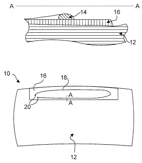
[031] FIG. 1 schematically illustrates a surface-mounted crack sensor 10
applied on a structural surface 12. In some embodiments the invention may
be applied to materials testing, in which case the structural surface 12 may
be
a side of a coupon of a material having a defined property, or a surface of a
test piece or model that is subjected to a test. Alternatively, the surface 12
may be on a critical structural surface of a structure in use. For example,
the
surface 12 may be on a critical component of an aerospace structure, a
motorized vehicle, a building, bridge, or tunnel, or on a pipe. The structural
surface 12 may be on a skin covering other components. The structural
surface 12 may have a wide variety of surface geometries.
[032] The surface-mounted crack sensor 10 includes an electrically
conductive paint or ink 14 applied on top of an undercoat 16 that acts as an
electrical insulator. The undercoat 16 is applied to the structural surface
12.
The electrically conductive paint or ink 14 is applied on the undercoat 16 to
define at least one trace 18 between a pair of terminals 20. The trace 18
passes
across a region on the surface 12 susceptible to cracking. The trace 18 of
electrically conductive paint or ink 14 and the undercoat 16 fracture
together,
if the structural surface 12 develops a crack that passes beneath the trace
18.
[0331 The undercoat 16 is composed of a cementitious compound, and
accordingly is brittle, i.e. it is susceptible to brittle fracture as opposed
to
CA 02638024 2008-07-22
WO 2007/085070 PCT/CA2006/001549
ductile fracture, and accordingly has a low percent elongation, very little
plastic or elastic deformation before fracturing, and the fracturing tends to
absorb little energy. The percent elongation of the cementitious compound is
less than .003 percent, preferably less than .001 percent, and most preferably
less than .0006 percent. The cementitious compound also has a low tensile
strength, less than 8,000 psi. Preferably the tensile strength is less than
5,000 psi, more preferably still, it is less than 2,000 psi. Most preferably
the
tensile strength of the cementitious compound is from 1 to 1500 psi, and still
has an aggressive bond to the structural surface 12. It will be appreciated
that the above-identified ranges are useful on surfaces of considerable
strength, and flexibility; with conductive inks and paints that have some
elasticity and strength; and for traces that are centimeters wide. In
different
scales, with different materials, and different applications, it will be
appreciated that cementitious compounds outside of these ranges may be
desirable.
[034] The undercoat 16 provides adequate bonding for a commercially
available conductive paint or ink, and an intended structural surface, and
further
provides electrical insulation between the conductive ink or paint, and the
structural surface, which, in some applications, is conductive.
[035] The undercoat 16 preferably has a fine particulate composition with a
binding agent so that the undercoat 16 readily crumbles with minimal shear
movement, but aggressively bonds to a wide variety of surfaces. Applicant has
found that certain ceramic-based materials having fine crystalline components
with a binder to provide an exemplary undercoat, although other particulate
compositions may also work. Cementitious compounds provide adequate
bonding of commercially available conductive paints and inks and a wide
variety
of surfaces, and further provide electrical insulation. High temperature
ceramic-
based compounds, such as those used for potting, casting or otherwise
covering thermocouples (herein called thermocouple cements), have been
found to have all of the desired properties for providing an insulating
undercoat.
Commercially available thermocouple cements have alumina, magnesia,
silica, and zirconia ceramic bases.
6
CA 02638024 2008-07-22
WO 2007/085070 PCT/CA2006/001549
[036] While not being limited by the following theory, it is believed that the
applicability of the cementitious compounds to surfaces in use under time-
varying loading, is in part due to their aggressive bonding to the surface 12.
The
surface 12 will normally flex and exhibit nominal, incidental, surface
deformations, resulting in cracking of the undercoat 16. These cracks will
naturally extend through the undercoat 16 substantially normal to the
surface 12. But for any reasonable thickness of the cementitious compounds
(generally a thin film is desired) a strength of a bond to the surface 12 will
prevent spalling and chipping, and so maintain integrity of a substantial part
of
the undercoat 16. This integrity is sufficient for maintaining required
support for
the trace 18, which is substantially more elastic and will not break if a thin
crack
in the undercoat 16 is produced. The break in the trace 18, is at least in
part
due to crumbling and effacement of the undercoat 16, which causes a persistent
gap considerably wider that the thin crack caused by normal flexure of the
surface 12. The crumbling and effacement favours that even if the crack in the
underlying structural surface 12 is closed at a time of measurement, the trace
18
will remain broken. This alleviates problems of failed detection in some
application environments, especially if interrogation of the surface-mounted
crack sensor 10 is most easily performed when the surface 12 is not under a
time-varying load.
[037] The undercoat 16 may be painted on, or applied in a number of ways
known in the art, for example using electrostatic deposition. For example it
may
be painted on by brush, roll, or spray. It may be applied through a template,
for
example made of silk screen-type material. The precise thickness of the
undercoat 16 need not be controlled for most applications because excess
thickness does not appreciably vary the brittleness of the undercoat 16 on one
hand, and because the undercoat 16 need only be thick enough to provide
electrical insulation as required by the application, on the other. In many
embodiments thinness is preferred to reduce a bulk added by the surface-
mounted crack sensor 10. Most cementitious compounds cease to have the
desired anti-spalling properties if applied in too great a thickness, and
cease to
have a desired electrical insulation if applied in too thin a coat, but most
7
CA 02638024 2008-07-22
WO 2007/085070 PCT/CA2006/001549
application methods will not produce a coat that approaches either of these
limits.
[038] In some applications the structural surface 12 is conductive, and the
undercoat 16 must be of a thickness and composition to provide adequate
electrical insulation between the structural surface 12 and the conductive ink
or
paint 14, to permit the detection of the test voltage applied across the trace
18
with a desired reliability. If the structural surface 12 is not conductive,
the
undercoat 16 need only be enough of an insulator so that conduction through
the undercoat 16 does not interfere with the measurement of the test voltage
resulting in an undesired reliability.
[039] The conductive ink or paint 14 may be applied over the undercoat 16
using any number of application techniques known in the art. These include:
using pens that allow for manual drawing of the trace 18; application (for
example, by roller, brush or spray) through a silk-screen or other template;
using
a stamp, for example, of rubber; application by an ink jet; and using a pad
printer
(with a roller or block). Using a pad printer, stamp or application through a
template, a pattern-form on a block, roller, template, or stamp is used to
define
the trace. It will be appreciated that depending on the surface to be used,
shape
of the pattern of the trace, accessibility constraints, surface properties,
etc.,
different methods of application may be preferred, and different surface
preparation steps may be required.
[040] The following are examples of commercially available conductive inks or
paints: acrylic resin containing metallic silver (e.g. Permatex Quick
GridT"^);
copper particle conductivity in a water based paint (e.g. CuPro-CoteTM paint);
silver filled, acrylic based paint; silver particle conductive epoxies; carbon
filled,
polyimide based paint; carbon filled, epoxy based paint; nickel-filled epoxy
based paint; silver powder in a methyl methacrylate binder ink; super shield
liquid format (also called nickel print): and acrylic base high purity nickel
flake
paint.
10411 The terminals=20 of the trace 18 can be formed of a tab, a recess or
other feature that permits coupling to a probe of an electronic interrogator.
The feature may be composed of another material that is secured to the
8
CA 02638024 2008-07-22
WO 2007/085070 PCT/CA2006/001549
surface 12 and/or undercoat 16, and makes reliable electrical connection with
the trace 18. In some embodiments the feature may be an area of the
trace 18 having a greater diameter.
10421 FIG. 2 is a schematic illustration of the surface-mounted crack
sensor 10 coupled to an exemplary embodiment of an electronic
interrogator for verifying continuity of the trace 18; a voltage detector 22.
The
voltage detector 22 may be a standard digital multimeter, for example, and
may have an interface for communicating a measurement outcome. This
communication may be provided by a visual display for a user in certain
situations, but in some applications it is preferable that the output be
provided
to an automated system, for example to a computer or a controller for
controlling automated equipment. The controller (such as an MTS Load
Frame controller) may control equipment used to test crack formation on the
surface 12. The computer or controller may be adapted to initiate failover
procedures and/or to issue system alarms in a system in use that incorporates
or relies on the structural surface, for example.
[043] The voltage detector 22 may be a multiport I/O card that can be
connected to multiple pairs of terminals, which is particularly useful if
multiple
terminals 20 are provided by the trace 18, or by multiple traces are provided.
Examples of patterns for applying the conductive ink or paint 14 to define
multiple terminals 20 are provided in FIG. 4.
[044] In operation, probes of the voltage detector 22 are coupled to the
terminals 20 of the surface-mounted crack sensor 10, resulting in a
determination of whether voltage is conducted there through. If the
surface 12 is cracked beneath the trace 18, conduction through the trace 18
will be broken, and substantially no voltage will be transmitted. Otherwise
the
trace 18 conducts voltage that is detected by the voltage detector 22,
indicating that the surface 12 is not cracked beneath the trace 18.
[045] The voltage detector 22 may be a dedicated part of a
materials/component testing apparatus, in which case it may be connected to
an equipment controller to halt or vary the testing of the material/component
in
response to crack formation, for example. The voltage detector 22 may be
9
CA 02638024 2008-07-22
WO 2007/085070 PCT/CA2006/001549
connected to the surface-mounted crack sensor 10 at a predetermined
interval to test the surface 12. The surface-mounted crack sensor 10 can
advantageously be used when visual inspection is difficult or undesirable.
[046] FIG. 3 is a schematic illustration of an embodiment of a surface-
mounted crack detection apparatus that includes surface-mounted
communications and processing electronics 24. Advantageously the
communications and processing electronics 24 may be of a kind that is
powered externally, via communications circuitry, so that there is no power
supply contained in the communications and processing electronics 24. This
largely facilitates embedding of the communications and processing
electronics 24 on the structural surface 12, as the communications and
processing electronics 24 can be paper thin, and of negligible mass (for many
applications). The communications and processing electronics 24 and
surface-mounted crack sensor 10 provide an integrated, closed detector that
can be painted over or rendered inaccessible in use, but remains available for
remote interrogation. One commercially available example of a
communications and processing device 24 powered by communications
circuitry is a radio frequency identification (RFID) tag. RFID tags are
available
that have memory and are capable of, for example, interrogating a
thermometer, and logging the measurements. Such a RFID tag could be
adapted for use in voltage detection.
[047] RFID tags generally are composed of a plastic film onto which a micro
chip and an antenna are attached. The antenna may be a spiral loop-type
antenna known in the art.
[048] A preferred connection between the terminals 20 and inputs of the
communications and processing device 24 uses an electrically conductive
epoxy because of its rigid connection, elasticity, and ease of application.
[049] In the preceeding examples, continuity of the trace 18 was determined
by connecting two terminals 20 to a voltage detector 22. A principal
advantage of using voltage detection is a low power requirement: by providing
a high impedance resistor in series with the surface-mounted crack sensor 10,
a low power continuity test of the circuit is provided. However, it will be
CA 02638024 2008-07-22
WO 2007/085070 PCT/CA2006/001549
appreciated by those of skill in the art that other electronic interrogators
could
equally be used to detect a crack through the surface-mounted crack
sensor 10 of FIG. 1. For example, a current through the trace 18, could be
used. The current could be detected directly, or by a voltage of a constant
current device well known in the art, for example. One advantage of current
detection is that the current will vary with a minimum cross-section of the
trace 18. The minimum cross-section being defined once the surface-
mounted crack sensor 10 is constructed, any decrease in the current (or any
increase in the voltage required to maintain a fixed current) corresponds to a
narrowing of the minimum cross-section. Accordingly, when current detection
is used, it is possible to determine a dimension of a crack running across
part
of the trace 18.
10501 FIG. 4 schematically illustrates an alternative embodiment of a surface-
mounted crack detector 25 that uses a micro chip 26 and creates an antenna
with the trace 18. In this embodiment, as before, a crack in the structural
surface 12 will sever the trace 18, but the manner in which this is detected,
according to the present invention, is via attempted energization of the micro
chip 26 through the antenna. The micro chip 26 is energized by the efficient
absorption of electromagnetic energy of a predetermined frequency (band) to
which the antenna is tuned. If the antenna is broken, the energy at the
predetermined frequency (band) will not be efficiently absorbed. As a result
the micro chip 26 will not be energized, and further, modulation of a side
band
of the electromagnetic energy re-emitted by the antenna for communication
will also be significantly impeded by the break in the antenna. As a result, a
failure of the micro chip 26 to respond indicates a crack.
[051] It should further be noted that in some applications of the invention,
the
micro chip 26 can be omitted. In these embodiments an eddy current probe
can be used to excite the antenna (trace 18), and a detected response would
indicate whether the electromagnetic energy at the predetermined frequency
(band) had been absorbed. If the electromagnetic energy was not absorbed,
it would be attributed to a break in the trace 18.
11
CA 02638024 2008-07-22
WO 2007/085070 PCT/CA2006/001549
[052] FIGs.5-7 schematically illustrate embodiments of surface-mounted
crack sensors that are interrogated by determining a capacitance produced
between the trace 18 and a charged surface or another trace 18. As is well
known in the art, when different charges build up on parallel plates that are
separated by an insulator, a capacitance is produced. The capacitance varies
directly with the surface area between the intersection of the surface areas
of
the two charged parts, inversely with a distance separating the charged parts,
and depends on a dielectric constant of a medium separating the charged
parts. A capacitance may be detected using a number of capacitance
detection circuits that typically involve oscillators and resistors, and these
capacitance detection circuits are typically tuned to a frequency that is
useful
for detecting the capacitance.
[053] It will further be appreciated that if the structural surface 12 is
conductive, and the undercoat 16 is a thin layer of an insulator, the surface
12
and surface-mounted crack sensor 10 define a capacitor, and this
capacitance can be used to determine whether the trace 18 is broken. If the
trace 18 is broken by an underlying crack, a signal applied between either
terminal 20 of the trace 18 and the surface 12 will detect a smaller
capacitance as a result of the smaller surface area of the capacitor. In
embodiments where effacement of the undercoat 16 effectively replaces the
undercoat with either a vacuum or air, this effacement only contributes to a
drop in the capacitance of the capacitor, because the dielectric constant of
air
and vacuum are higher than that of most solids, including the cementitious
compound. In some embodiments the effacement may produce a detectable
drop in capacitance even before the trace 18 is entirely broken, especially if
the trace 18 is particularly fat, and there are many points of effacement. In
these embodiments, if different capacitance values are observed depending
on which terminal 20 is supplied the voltage, or such a capacitance value is
different than a reference value, a break in the trace 18 is detected.
Circuitry
for determining a capacitance is well known in the art, and typically includes
a
tuned oscillator circuit.
12
CA 02638024 2008-07-22
WO 2007/085070 PCT/CA2006/001549
[054] FIG. 5 schematically illustrates an embodiment of a surface-mounted
crack sensor 30 that consists of two brittle layers. In ghost view, a
rectangular
trace 18 is painted across the undercoat 14, as described above. A
terminal 32 is provided for electrical connection with the rectangular trace
18.
The rectangular trace 18 is overlaid by a second coat 34 of cementitious
compound, which may be a same cementitious compound applied to produce
the undercoat 14. The second coat 34 provides a surface for receiving a
parallel trace 36. The parallel trace 36 provides a terminal 20 for connection
to a capacitance detector.
[055] It will be appreciated by those of skill in the art that in alternative
embodiments a same stamp can be used to form both the trace 18 and the
parallel trace 36, which may be preferably superimposed to maximize the
capacitance.
10561 An advantage of the pattern of the parallel trace 36 is that the
capacitance detected will decrease in steps each time the crack (originating
at
the edge) traverses a respective segment of the parallel trace 36, allowing a
graded assessment of the integrity of the structural surface 12.
[057] It will be noted that the rectangular trace 18 and parallel trace 36
could
be switched as the cracks will pass through the multiple layers of the
cementitious compound together.
[0581 FIG. 6 schematically illustrates an alternative layer for a capacitance-
interrogated surface-mounted crack sensor 40. The capacitance is produced
between the trace 18 (visible in ghost view) and a conductive surface 42 that
is applied over the trace 18. The trace 18 is connected to terminal 20, and
the
conductive surface 42 is connected to a terminal 44. The surface-mounted
crack sensor 40 shown has a second coat 34 to provide the insulation
between the trace 18 and the conductive surface 42.
1059] While any conductive surface 42 may be used, applicant contemplates
the use of a coated film or tape 46, such as Physical Vapour Deposition
(PVD) tape, to provide the conductive surface 42. PVD tape has a metallized
coating on a body of an insulating plastic. As the tape 46 may have
significant
tensile strength and elasticity, in which case it would not be expected to
13
CA 02638024 2008-07-22
WO 2007/085070 PCT/CA2006/001549
fracture with the underlying crack. Whether or not the tape breaks, the
surface area of the capacitor depends on the a surface area of intersection of
the two charged plates (projected into a common plane), and accordingly, a
brake in the trace 18 will reduce the capacitance.
[060] It will be appreciated by those of skill in the art that the second coat
34
could be replaced by other insulating layers, such as the body 46 of a tape
which provides the conductive surface 42 on a top side, rather than a bottom
side as shown. One advantage of this would be an even separation of the
trace 18 and the conductive surface 42. However, it will be necessary to
prevent bonding of the trace 18 to the tape, which could otherwise adhere to
the tape and not break with the undercoat 16.
10611 FIG. 7 schematically illustrates a single-layer capacitance-interrogated
surface-mounted crack sensor 50. Surface-mounted crack sensor 50 is
composed of the same cementitious compound undercoat 16 as in previous
embodiments, however there are two traces 18a and 18b which remain in
parallel configuration. Effectively the capacitance produced between
traces 18a,b is a property of the length of the parallel segments that are
charged. If successive segments of trace 18a or trace 18b are broken, the
capacitance measured between corresponding terminals 20 will drop.
[062] The foregoing embodiments of surface-mounted crack sensors are not
intended to be exhaustive, the range of specific crack sensors provided show
how the cementitious compound can be used with conductive ink or paint to
produce surface-mounted crack sensors.
[063] FIG. 8 is a schematic illustration of a set of templates that could be
used to apply one or more traces 18. Two of the templates provide for
application in a place where cracks are expected in a given direction. For
example, cracks are frequently expected to develop along edges of surfaces,
and work their way into the surface in a direction orthogonal to the edge. In
such a case, traces will logically be arranged to extend parallel to the edge.
Here parallel traces can be used to determine a dimension of the crack. For
example, knowing which traces have ruptured, and which have not may
provide bounds for a size of the crack. This can be useful in testing to
ensure
14
CA 02638024 2008-07-22
WO 2007/085070 PCT/CA2006/001549
that a crack in a test piece has grown to a predetermined size before
automatically ending the test, or to enforce a safe operating regime that
tolerates a certain number of cracks of certain dimensions. Alternatively
multiple traces can be used to determine a position of the crack.
[064] A sensitivity of the surface-mounted crack sensor can be defined by a
thickness of the trace. The crack may only be detected if it spans the
thickness of the trace, and so the surface-mounted crack sensor can be made
of a desired sensitivity as well as of a desired spatial arrangement.
[065] If cracks are expected to form radially from a point, for example,
surrounding a single point attachment (such as a rivet), azimuthally extended
traces can be provided. As before a sequence of azimuthally extended traces
to provide an indicator of a size of the crack.
[066] FIG. 9a is an image of a surface-mounted crack sensor defined using a
template of FIG. 8. The surface-mounted crack sensor has four traces
encircling a region, defined by five terminals. The trace is composed of MG
Chemicals Silver Print TM, and the undercoat is composed of Omega CCTM
high temperature ceramic-based cement.
[067] FIG. 9b is an image of a silk screen template of a second shape shown
in FIG. 8, prior to application of MG Chemicals Nickel Print T"' The silk
screen
template defines one trace encircling a region between two terminals, by
masking a remainder of an undercoat of Omega CCTM high temperature
ceramic-based cement. FIG. 9c is an image of a surface-mounted crack
sensor produced after application of the MG Chemicals Nickel Print TM
[068] The undercoats of the surface-mounted crack sensors were tested
prior to application of the conductive ink or paint to ensure adequate
electrical
insulation is provided throughout the surface where the traces were to be
deposed.
EXAMPLE
10691 The circuit diagram shown in FIG. 10 was used to verify the principle of
the invention. The sensing circuit used a 10-volt DC power supply, which was
CA 02638024 2008-07-22
WO 2007/085070 PCT/CA2006/001549
connected to an analogue input of a computerized MTS load frame controller.
The MTS load frame controller can be set to "alarm" (notify the operator by
displaying a warning message) or autonomously "halt" a command program
sequence immediately upon detecting a pre-set change in the signal on the
analogue input circuit. When the voltage on the analog input dropped below 9
volts, the MTS load frame controller halted the test and stopped the cyclic
loading. A lap joint shown in FIG. 11 stopped after 280,000 cycles.
10701 FIG. 11 is an image of a riveted, lap jointed, aluminum test coupon
upon which a surface-mounted crack detection apparatus has been affixed.
The undercoat was a manually painted on layer of Omega CCTM high
temperature ceramic-based cement. The undercoat was found to be about
5/1000ths of an inch thick. The electrically conductive paint used was
Permatex Quick GridTM, an acrylic resin containing metallic silver, which was
also painted on manually.
[071] FIG. 12 is an enlarged image of a crack formed through the aluminum
test coupon.
[072] It will be appreciated that the surface-mounted sensor according to the
invention can be customized to any complex shape and bridge across built-up
constructs composed of a mix of differing materials.
16