Note: Descriptions are shown in the official language in which they were submitted.
CA 02639203 2008-08-29
MOBILE WIRELESS COMMUNICATIONS DEVICE INCLUDING A FOLDED
MONOPOLE MULTI-BAND ANTENNA AND RELATED METHODS
Field of the Invention
The present invention relates to the field of communications systems, and,
more
particularly, to mobile wireless communications devices and antennas therefor,
and related
methods.
Background of the Invention
One challenge in the development of antennas for mobile handheld devices, such
as cellular devices, is the balance between the antenna size and its
performance. On one
hand, users have come to expect smaller and relatively stylish devices with no
visible
antenna structure, which imposes restrictions on the device form factor and
thus the
available antenna size. On the other hand, users expect devices with an
antenna that
efficiently supports the various wireless communications standards. Yet, this
requires that
the antenna has a reasonable size to achieve requisite performance often over
multiple
operating frequency bands. See, e.g., Geyi, "Physical Limitations of Antenna,"
IEEE
Transactions on Antennas and Propagation, vol. AP-51, pages 2116-2123, 2003.
Planar inverted-F antennas (PIFAs) are commonly used for handheld devices.
However, PIFAs typically have relatively narrow bandwidths. To overcome this
shortcoming, various techniques are sometimes used to increase the effective
bandwidth of
PIFAs, such as using parasitic elements, additional shorting pins, etc. Yet,
such structures
can unduly complicate the antenna structure and increase its cost. See, e.g.,
U.S. Patent
No. 7,023,387; Liu et al., "Dual-Frequency Planar Inverted-F Antenna," IEEE
Transactions on Antennas and Propagation, vol. 45, no. 9, pages 1451-1457,
October
1997; Rowell et al., "A Compact PIFA Suitable for Dual-Frequency 900/1800-Mhz
Operation," IEEE Transactions on Antennas and Propagation, vol. 46, pages
586598, Apr.
1998; Guo et al., "Miniature Built-In Quad-Band Antennas for Mobile Handsets,"
IEEE
Antennas Wireless Propagation. Letters, vol. 2, pages 30-32, 2003.
Another form of antenna, i.e., the monopole antenna, typically has a
relatively
wider bandwidth as compared with that of a PIFA. However, a significant
drawback of
such monopole antennas is that they typically require more surface area (i.e.,
they are
larger) than a comparable PIFA. Another drawback of monopole antennas is that,
due in
1
CA 02639203 2008-08-29
part to the size constraints, they are typically implemented as external
antennas, whereas a
PIFA is easier to implement as an internal antenna.
Even so, another advantage that a 2D monopole antenna has over the PIFA, in
addition to its wideband response, it has a low profile, is simpler to design,
and less
expensive to fabricate.
One exemplary monopole antenna arrangement is set forth in U.S. Patent No.
6,054,955 to Schlegel, Jr., et al. The antenna arrangement is for use in the
housing of a
portable communications device, such as a laptop. The antenna arrangement
includes a
pair of spaced folded monopole antennas in 2D. Each antenna includes a first
printed
circuit board having a conducting surface that forms a ground plane. Mounted
on the first
circuit board is a second printed circuit board having a right-angled strip of
conducting
material, which forms a folded monopole radiating element. The folding of the
monopole
reduces its height, to thereby enable it to fit into small casings and the
like. To compensate
for the effects of the folded monopole on the electrical match, frequency
bandwidth and
electromagnetic fields, a shunt inductance is introduced between the monopole
and the
ground plane. The antennas are mounted within cavities that can be lined or
coated with
metallic material, to improve the radiation patterns of the antennas and
isolate them from
the electronic components of the communications system.
Despite the existence of such antenna arrangements, further advancements in
monopole antenna structures for mobile wireless communications devices may be
desirable in some applications.
Brief Description of the Drawings
FIG. 1 is a schematic block diagram of a mobile wireless communications device
in accordance with an exemplary embodiment including a folded monopole antenna
(FMA).
FIG. 2 is a top perspective view of a printed circuit board (PCB) with a
folded
monopole antenna thereon in accordance with one aspect.
FIG. 3 is a bottom perspective view of the PCB and folded monopole antenna of
FIG. 2.
FIG. 4 is a rotated top perspective view of the PCB and folded monopole
antenna
of FIG. 2.
2
CA 02639203 2008-08-29
FIG. 5 is a 2D plan view (i.e., unfolded) of the conductive trace of the
folded
monopole antenna of FIG. 2.
FIGS. 6A and 6B are enlarged perspective views of the dielectric body of the
folded monopole antenna as seen in FIGS. 2 and 3, respectively, with the
conductive trace
removed.
FIG. 7 is a graph of return loss vs. frequency for an embodiment of the
antenna of
FIG. 2.
FIG. 8 is a measured radiation pattern diagram for an embodiment of the
antenna
of FIG. 2 at 919 MHz.
FIG. 9 is a measured radiation pattern diagram for an embodiment of the
antenna
of FIG. 2 at 1.97 GHz.
FIG. 10 is a schematic block diagram illustrating exemplary components of a
mobile wireless communications device in which the folded monopole antenna of
FIG. 2
may be used.
Detailed Description of the Preferred Embodiments
The present description is made with reference to the accompanying drawings,
in
which preferred embodiments are shown. However, many different embodiments may
be
used, and thus the description should not be construed as limited to the
embodiments set
forth herein. Rather, these embodiments are provided so that this disclosure
will be
thorough and complete. Like numbers refer to like elements throughout.
Generally speaking, a mobile wireless communications device is disclosed
herein
which may include a portable housing, a printed circuit board (PCB) carried
within the
portable housing, and wireless communications circuitry carried by the PCB
within the
portable housing. Furthermore, the device may also include a folded monopole
antenna
assembly. More particularly, the folded monopole antenna assembly may include
a
dielectric body adjacent the PCB and having a generally rectangular shape
defining
opposing top and bottom faces, opposing first and second end faces, and
opposing first
and second side faces. The antenna assembly may also include a conductive
trace coupled
to the wireless communications circuitry having a first end section extending
along the
first end face, a second end section extending along the second end face, and
an
intermediate section extending along the top, bottom, first side and second
side faces.
3
CA 02639203 2008-08-29
In addition, the conductive trace may further include at least one conductive
impedance matching patch coupled to the intermediate section. In some
embodiments, the
at least one conductive impedance matching patch may comprise a plurality of
spaced-
apart impedance matching patches. The at least one conductive impedance
matching patch
may extend along one or more of the top face, the first and second end faces,
and the first
and second side faces.
The first end section may define a feed point for the conductive trace.
Furthermore,
the first and second side faces may have greater widths than the first and
second end faces.
By way of example, the wireless communications circuitry may comprise a
cellular
transceiver. Also, the conductive trace may operate over a plurality of radio
frequency
(RF) communications bands.
A folded monopole antenna assembly for a mobile wireless communications
device and method for making the same are also provided. The method may
include
forming a dielectric body having a generally rectangular shape defining
opposing top and
bottom faces, opposing first and second end faces, and opposing first and
second side
faces. The method may further include forming a conductive trace on the
dielectric body
having a first end section extending along the first end face, a second end
section
extending along the second end face, and an intermediate section extending
along the top,
bottom, first side and second side faces.
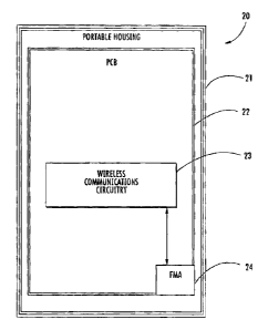
Referring initially to FIGS. 1-6B, a mobile wireless communications device 20
illustratively includes a portable housing 21, a printed circuit board (PCB)
22 carried
within the portable housing, and wireless communications circuitry 23 carried
by the PCB
within the portable housing. The wireless communications circuitry 23 is
carried on a top
dielectric layer 25 of the PCB 22 (FIG. 2), and the PCB also has a ground
plane 26 on a
bottom side thereof (FIG. 3) opposite the top dielectric layer. By way of
example, the
wireless communications circuitry 23 may comprise cellular communications
circuitry,
e.g., a cellular transceiver. Other wireless communications circuitry, such as
wireless local
area network (WLAN) and satellite positioning (e.g., GPS) communications
circuitry, may
also be used, as will be discussed further below.
The device 20 further illustratively includes a folded monopole antenna
assembly
24. In particular, the folded monopole antenna assembly 24 illustratively
includes a
dielectric body or frame 30 adjacent the PCB 22 and having a generally
rectangular shape
defining opposing top and bottom faces 35 and 36, opposing first and second
end faces 37
4
CA 02639203 2008-08-29
and 38, and opposing first and second side faces 39 and 40 (see FIGS. 6A and
6B). It
should be noted that although the edges of the body 30 are shown as being 90
(i.e.,
squared off), these edges/corners may be rounded, etc., in some embodiments.
The antenna assembly 24 also illustratively includes a conductive trace
coupled to
the wireless communications circuitry 23 having a first end section 41
extending along the
first end face 37, a second end section 42 extending along the second end face
38, and an
intermediate section 43 extending along the top, bottom, first side and second
side faces
35, 36, 39 and 40. The conductive trace defines a folded monopole antenna
element, the
unfolded two-dimensional (2D) structure of which is shown in FIG. 5.
In the illustrated example, the conductive trace further includes three
conductive
impedance matching patches Pl, P2, and P3 spaced-apart along the conductive
trace and
coupled to the intermediate section 43, as shown. It should be noted that in
other
embodiments, however, different numbers, shapes, and/or placements of
impedance
matching patches may be used, or none at all. In the present example, the
patch Pl is on
the second side face 40, the second patch P2 is on the top face 35 and the
first side face 39,
and the third patch P3 is on the first side face 39 and the second end face
38. The patches
Pl, P2, and P3 advantageously improve matching for the low and high frequency
bands, as
will be appreciated by those skilled in the art.
In one embodiment, the wireless communications circuitry 23 includes cellular
transmitter/receiver circuitry for communicating over a plurality of cellular
communications bands. By way of example, such cellular bands may include
Global
System for Mobile communication (GSM), International Mobile Telecommunications-
2000 (IMT), Universal Mobile Telecommunications System (UMTS), Digital
Communication Services (DCS), and/or Personal Communication Services (PCS)
bands.
However, other types of wireless radio frequency (RF) communications circuitry
(e.g.,
Bluetooth/802.11 WLAN circuitry), may also be electrically coupled to the
folded
monopole antenna assembly 24 in different embodiments, as well as satellite
positioning
receiver circuitry (e.g., GPS, Galileo, GLONASS, etc.).
The folded monopole antenna assembly 24 advantageously provides the multi-
band and compact characteristics of a PIFA, as well as the broadband,
environmental
isolation, and simplicity characteristics of a monopole antenna. In one
exemplary
embodiment, the antenna 24 supports at least six frequency bands (i.e., hex-
band),
although other numbers of bands may be supported in different embodiments.
More
CA 02639203 2011-06-22
particularly, in this exemplary embodiment the antenna assembly 24 supports
GSM
800/900/1800/1900, IMT-2000, UMTS 2200, DCS/PCS 1800/1900, Bluetooth 2400, and
WLAN 2450, as shown in the measured return loss vs. frequency graph of FIG. 7.
The
measured radiation pattern for the exemplary hex-band antenna 24 at operating
frequencies of 919 MHz and 1.97 GHz are shown in FIGS. 8 and 9, respectively.
In the exemplary embodiment, a length L of the conductive trace 27 is a
quarter
wavelength at about 800 MHz, although different length-to-wavelength ratios
are also
possible in different embodiments. The length L controls the fundamental
resonating
mode of the antenna 24, as will be appreciated by those skilled in the art.
The modes at
higher frequencies are generated at various portions of this length. The 3D
wrapping of the
antenna around the dielectric body 30 controls the current distribution along
the monopole
length L, and thus controls the electrical length(s) for the higher resonant
frequency
band(s) as well as antenna bandwidth, as will also be appreciated by those
skilled in the
art.
Referring to Figure 3, it can be seen that a portion of the conductive trace
43 is
folded around the edge of the PCB 22 and secured to the underside of the PCB
22 at a
location that is proximate to the bottom of the folded monopole antenna
assembly 24.
Those of skill in the art will appreciate that mounting the conductive trace
43 this
configuration provides spacing between the top and bottom portions of the
conductive
trace 43 equal to the combined thicknesses of the PCB 22 and the dielectric
body 40,
thereby providing enhanced performance with a very compact structural
assembly.
In the exemplary implementation, the antenna assembly 24 has dimensions of
10mm x 20mm x 8.5mm, the ground plane 26 has dimensions of 55mm x 87mm, and a
1.5mm thick FR-4 dielectric ground plane 25 with relative permittivity 4.4 may
support
the antenna and the ground plane. However, it will be appreciated by those
skilled in the
art that other dimensions and/or materials may be used in different
embodiments.
The antenna assembly 24 therefore advantageously provides broadband operation
in the supported frequency bands. The relatively small size of the antenna
assembly 24
results from "wrapping" the conductive trace 43 into the above-described 3D
structure,
which provides a relatively compact structure in addition to a relatively
simplicity due to
the fact that it is a monopole antenna. Moreover, the antenna assembly 24
advantageously
provides desired matching properties at the supported frequency bands without
the need
for additional matching circuitry, although such circuitry may be used in some
6
CA 02639203 2011-06-22
embodiments if desired, as will be appreciated by those skilled in the art.
The 3D shape of
the antenna assembly 24 not only significantly reduces the antenna size, but
it may also
provide radiation pattern diversity as well.
A method for making the folded monopole antenna 24 may include forming the
dielectric body 30 having a generally rectangular shape defining opposing top
and bottom
faces 35 and 36, opposing first and second end faces 37 and 38, and opposing
first and
second side faces 39 and 40. The method may further include forming a
conductive trace
27 on the dielectric body 30 having a first end section 41 extending along the
first end face
37, a second end section 42 extending along the second end face 38, and an
intermediate
section extending along the top, bottom, first side and second side faces 35,
36, 39, and 40.
It should be noted that in some embodiments the conductive trace 27 may be
etched on a
supporting dielectric surface, as will be appreciated by those skilled in the
art.
Exemplary components of a hand-held mobile wireless communications device
1000 in which the antenna 24 may be used are further described below with
reference to
FIG. 10. The device 1000 illustratively includes a housing 1200, a keypad 1400
and an
output device 1600. The output device shown is a display 1600, which is
preferably a full
graphic LCD. Other types of output devices may alternatively be utilized. A
processing
device 1800 is contained within the housing 1200 and is coupled between the
keypad 1400
and the display 1600. The processing device 1800 controls the operation of the
display
1600, as well as the overall operation of the mobile device 1000, in response
to actuation
of keys on the keypad 1400 by the user.
The housing 1200 may be elongated vertically, or may take on other sizes and
shapes (including clamshell housing structures). The keypad may include a mode
selection
key, or other hardware or software for switching between text entry and
telephony entry.
[0029] In addition to the processing device 1800, other parts of the mobile
device
1000 are shown schematically in FIG. 10. These include a communications
subsystem
1001; a short-range communications subsystem 1020; the keypad 1400 and the
display
1600, along with other input/output devices 1060, 1080, 1100 and 1120; as well
as
memory devices 1160, 1180 and various other device subsystems 1201. The mobile
device
1000 is preferably a two-way RF communications device having voice and data
communications capabilities. In addition, the mobile device 1000 preferably
has the
capability to communicate with other computer systems via the Internet.
7
CA 02639203 2011-06-22
Operating system software executed by the processing device 1800 is preferably
stored in a persistent store, such as the flash memory 1160, but may be stored
in other
types of memory devices, such as a read only memory (ROM) or similar storage
element.
In addition, system software, specific device applications, or parts thereof,
may be
temporarily loaded into a volatile store, such as the random access memory
(RAM) 1180.
Communications signals received by the mobile device may also be stored in the
RAM
1180.
The processing device 1800, in addition to its operating system functions,
enables
execution of software applications 1300A-1300N on the device 1000. A
predetermined set
of applications that control basic device operations, such as data and voice
communications 1300A and 1300B, may be installed on the device 1000 during
manufacture. In addition, a personal information manager (PIM) application may
be
installed during manufacture. The PIM is preferably capable of organizing and
managing
data items, such as e-mail, calendar events, voice mails, appointments, and
task items. The
PIM application is also preferably capable of sending and receiving data items
via a
wireless network 1401. Preferably, the PIM data items are seamlessly
integrated,
synchronized and updated via the wireless network 1401 with the device user's
corresponding data items stored or associated with a host computer system.
Communication functions, including data and voice communications, are
performed through the communications subsystem 1001, and possibly through the
short-
range communications subsystem. The communications subsystem 1001 includes a
receiver 1500, a transmitter 1520, and one or more antennas 1540 and 1560. In
addition,
the communications subsystem 1001 also includes a processing module, such as a
digital
signal processor (DSP) 1580, and local oscillators (LOs) 1601. The specific
design and
implementation of the communications subsystem 1001 is dependent upon the
communications network in which the mobile device 1000 is intended to operate.
For
example, a mobile device 1000 may include a communications subsystem 1001
designed
to operate with the MobitexTM, Data TACTM or General Packet Radio Service
(GPRS)
mobile data communications networks, and also designed to operate with any of
a variety
of voice communications networks, such as AMPS, TDMA, CDMA, WCDMA, PCS,
GSM, EDGE, etc. Other types of data and voice networks, both separate and
integrated,
may also be utilized with the mobile device 1000. The mobile device 1000 may
also be
compliant with other communications standards such as 3GSM, 3GPP, UMTS, etc.
8
CA 02639203 2011-06-22
Network access requirements vary depending upon the type of communication
system. For example, in the Mobitex and DataTAC networks, mobile devices are
registered on the network using a unique personal identification number or PIN
associated
with each device. In GPRS networks, however, network access is associated with
a
subscriber or user of a device. A GPRS device therefore requires a subscriber
identity
module, commonly referred to as a SIM card, in order to operate on a GPRS
network.
When required network registration or activation procedures have been
completed, the mobile device 1000 may send and receive communications signals
over the
communication network 1401. Signals received from the communications network
1401
by the antenna 1540 are routed to the receiver 1500, which provides for signal
amplification, frequency down conversion, filtering, channel selection, etc.,
and may also
provide analog to digital conversion. Analog-to-digital conversion of the
received signal
allows the DSP 1580 to perform more complex communications functions, such as
demodulation and decoding. In a similar manner, signals to be transmitted to
the network
1401 are processed (e.g. modulated and encoded) by the DSP 1580 and are then
provided
to the transmitter 1520 for digital to analog conversion, frequency up
conversion, filtering,
amplification and transmission to the communication network 1401 (or networks)
via the
antenna 1560.
In addition to processing communications signals, the DSP 1580 provides for
control of the receiver 1500 and the transmitter 1520. For example, gains
applied to
communications signals in the receiver 1500 and transmitter 1520 may be
adaptively
controlled through automatic gain control algorithms implemented in the DSP
1580.
In a data communications mode, a received signal, such as a text message or
web
page download, is processed by the communications subsystem 1001 and is input
to the
processing device 1800. The received signal is then further processed by the
processing
device 1800 for an output to the display 1600, or alternatively to some other
auxiliary I/O
device 1060. A device user may also compose data items, such as e-mail
messages, using
the keypad 1400 and/or some other auxiliary I/O device 1060, such as a
touchpad, a rocker
switch, a thumb-wheel, or some other type of input device. The composed data
items may
then be transmitted over the communications network 1401 via the
communications
subsystem 1001.
In a voice communications mode, overall operation of the device is
substantially
similar to the data communications mode, except that received signals are
output to a
9
CA 02639203 2011-06-22
speaker 1100, and signals for transmission are generated by a microphone 1120.
Alternative voice or audio 110 subsystems, such as a voice message recording
subsystem,
may also be implemented on the device 1000. In addition, the display 1600 may
also be
utilized in voice communications mode, for example to display the identity of
a calling
party, the duration of a voice call, or other voice call related information.
The short-range communications subsystem enables communication between the
mobile device 1000 and other proximate systems or devices, which need not
necessarily
be similar devices. For example, the short-range communications subsystem may
include
an infrared device and associated circuits and components, or a BluetoothTM
communications module to provide for communication with similarly-enabled
systems
and devices.
Many modifications and other embodiments will come to the mind of one skilled
in the art having the benefit of the teachings presented in the foregoing
descriptions and
the associated drawings. Therefore, it is understood that various
modifications and
embodiments are intended to be included within the scope of the appended
claims.