Note: Descriptions are shown in the official language in which they were submitted.
CA 02639498 2008-09-11
MBM File 1308-108
DEVICE AND PIXEL ARCHITECTURE FOR
HIGH RESOLUTION DIGITAL IMAGING
FIELD OF THE INVENTION
[0001] The present invention pertains to the field of active pixel sensor
arrays, and in
particular to a charge-gated transistor device and high-resolution imagers
employing
active pixel sensor architectures.
BACKGROUND
[0002] The term digital imaging refers to the function of a system capable
of
producing a digital electronic image from optical image information. Such a
system is
usually consisted of a matrix of pixelated optical detectors each associated
with their own
electronic circuits (which together are called pixels), connected to
peripheral circuits
(biasing, addressing, readout and digitizer circuitries).
[0003] One of the commonly used architectures for large area imaging is the
passive
pixel sensor (PPS) shown in figure 1.a. Here, a detector, for example, an
amorphous
selenium (a-Se) based photoconductor, a Cesium Iodide (CsI) phosphor coupled
to an
amorphous silicon (a-Si:H) p-i-n photodiode, or even a crystalline p-n
junction, is
integrated with a readout circuit comprising a transistor switch such as an a-
Si:H thin-
film transistor (TFT). Signal charge is accumulated on the pixel sensor during
an
integration cycle and is transferred to an external charge amplifier via the
transistor
switch, Ts, during a readout/reset cycle. The transferred charge is converted
to an
equivalent voltage in the charge amplifier and is then further processed
(using sampling
and/or digitization) towards reconstruction of a digital image. It is noted
that the pixel
capacitance mentioned above is the p-i-n photodiode capacitance or an
integrated storage
capacitor for the a-Se photoconductor arrangement, or the p-n junction
capacitance. Other
additional analog signal processing sequences are also possible, for example,
double
sampling mechanisms are typically used to correct for the effect of non-
uniformities
within the circuitry. These non-uniformities may comprise process non-
uniformities in
1
CA 02639498 2008-09-11
MBM File: 1308-108
the form of offsets, and, in the case of a-Si:H technology, non-uniformities
in pixel
circuit performance due to transistor instability. For example, International
Patent
Application Publication Nos. W09634416 and W09705659 further disclose flat-
panel
detectors for radiation imaging using PPS architecture.
[0004] While the PPS has the advantage of being compact and therefore
suitable for
high-resolution imaging, reading a small output signal of the PPS for low
input optical
signal results in a noisy voltage at the output of the charge integrator, due
to the fact that
charge integrators potentially add a considerable amount of noise to the input
signal. This
lowers the signal-to-noise ratio (SNR) at low signal levels, and thus,
degrades the pixel
dynamic range.
[0005] One approach for improved SNR is disclosed in International Patent
Application Publication No. W002067337 indicating that the SNR can be
increased by
employing in-situ, or pixel, amplification via an a-Si:H current-mediated
active pixel
sensor (C-APS) as depicted in figure 1.b. Reported gain, linearity and noise
performance
show an improvement and indicate that the a-Si:H C-APS, coupled with an
established x-
ray detection technology such as a-Se or CsI/p-i-n photodiodes, can meet the
stringent
requirements for low noise digital x-ray imaging for applications such as
fluoroscopy,
which no more than 1000 electrons of noise are allowed. In C-APS architecture,
T2 is
used to reset the voltage of the detector, and an on-pixel transconductance
amplifier (Ti)
converts the detector voltage to an equivalent output current, which is then
integrated in
the column charge amplifier. The advantage of C-APS to PPS is the high gain;
since the
pixel capacitor is not discharged, a constant output current is provided as
long as the row
select transistor, T3, is on. Double sampling is necessary in C-APS to remove
effects of
non-uniformities among pixels.
[0006] Another approach disclosed in International Patent Application
Publication No.
W002067337 reports a near-unity gain pixel amplifier, namely, an a-Si:H
voltage-
mediated active pixel sensor (V-APS). A V-APS architecture is illustrated in
figure 1 c.
The pixel configuration is exactly similar to that of C-APS architecture,
however, in V-
2
CA 02639498 2008-09-11
MBM File. 1308-108
APS, the pixel output is the detector voltage which is buffered out by the
pixel amplifier.
The advantage of V-APS over PPS and C-APS is that the charge amplifier is
replaced by
a simple voltage buffer. This helps less complicated design and less expensive
implementation of peripheral circuits. Like the C-APS, double sampling
mechanisms can
be applied to the V-APS to correct for the effect of non-uniformities within
the circuitry.
[0007] A
difference between C-APS and V-APS is in pixel output signal, i.e., current
versus voltage, the pixel circuit of both architectures (figures 1.b and 1.c)
is otherwise the
same, and is the basic structure of active pixel architecture, comprising
three field effect
transistors. Other variations of the basic architectures have been reported to
improve
functionality of the circuit. For example, International Patent Application
Publication No.
W02000019706 disclose methods of high speed resetting of the pixel, or as
another
example, International Patent Application Publication No. W02006042407
introduces
multimode architectures for high dynamic range, and low noise imaging
applications as
illustrated in figure 2.a; a four-transistor approach. Other non classical
architectures such
as two-transistor multimode architectures have also been reported in F.
Taghibakhsh,
K.S. Karim, "High dynamic range 2-TFT amplified pixel sensor architecture for
digital
mammography tomosynthesis" JET Circuits Devices & Systems, vol. 1, no. 1, pp.
87-92,
(2007), and F. Taghibakhsh, K.S. Karim, "Amplified Pixel Sensor Architectures
for Low
Dose Computed Tomography using Silicon Thin Film Technology", Proceedings of
SPIE, vol. 6510, (2007). These architectures are shown in figure 2.b, where
addressing
each row is performed by providing a separate bias voltage for the entire row.
Although
such architectures provide smaller pixel size for higher imaging resolution,
they require
more complex peripheral circuits, and non standard driving methods. In this
architecture,
the row select (or read) transistor has been transferred from each pixel to
its row. In all
APS architectures at least three transistors are distinguished: 1) a
transconductance
amplifying transistor (Ti) that its gate is connected to the pixel
sensor/detector element,
2) a reset transistor (T2) that presets the voltage of the pixel
sensor/detector element,and,
and 3) a row select (or read) transistor (T3) that connects drain or source of
the
amplifying transistor to the imager matrix bus lines.
3
CA 02639498 2008-09-11
MBM File: 1308-108
[0008] This background information is provided for the purpose of making known
information believed by the applicant to be of possible relevance to the
present invention.
No admission is necessarily intended, nor should be construed, that any of the
preceding
information constitutes prior art against the present invention.
SUMMARY OF THE INVENTION
[0009] An object of the present invention is to provide a device and pixel
architecture
for high resolution digital imaging. In accordance with an aspect of the
present invention,
there is provided a digital imaging apparatus comprising: a detector for
generating a first
signal in response to photons incident thereupon; and readout circuitry
operatively
coupled to the detector, said readout circuitry configured to generate a
second signal
representative of said first signal, said readout circuitry including an
electron device
comprising: a field effect transistor having a gate terminal, a drain terminal
and a source
terminal; and a conductor plate capacitively coupled to the gate terminal of
said field
effect transistor, wherein current flowing between the drain and source
terminals of said
field effect transistor can be modulated by a voltage applied to said
conductor plate and
by an electric charge residing on the gate terminal of said field effect
transistor.
[0010] In accordance with another aspect of the present invention, there is
provided a
digital imaging system comprising an array of digital imaging apparatuses,
each digital
imaging apparatus comprising: a detector for generating a first signal in
response to
photons incident thereupon; and readout circuitry operatively coupled to the
detector, said
readout circuitry configured to generate a second signal representative of
said first signal,
said readout circuitry including an electron device comprising: a field effect
transistor
having a gate terminal, a drain terminal and a source terminal; and a
conductor plate
capacitively coupled to the gate terminal of said field effect transistor,
wherein current
flowing between the drain and source terminals of said field effect transistor
can be
modulated by a voltage applied to said conductor plate and by an electric
charge residing
on the gate terminal of said field effect transistor.
4
CA 02639498 2008-09-11
MBM File 1308-108
[0011] In accordance with another aspect of the present invention, there is
provided a
method of operating one or more selected digital imaging apparatuses in an
array thereof,
the method comprising capacitively applying an addressing signal to the gate
of a
transistor of each selected digital imaging apparatus.
[0012] In accordance with another aspect of the present invention, there is
provided an
electron device comprising a field effect transistor having a gate terminal, a
drain
terminal and a source terminal; and a conductor plate capacitively coupled to
the gate
terminal of said field effect transistor, wherein current flowing between the
drain terminal
and the source terminal of said field effect transistor can be modulated by a
voltage
applied to said conductor plate and by an electric charge residing on the gate
terminal of
said field effect transistor.
[0013] In accordance with another aspect of the invention, there is
provided a single-
transistor active pixel architecture for high resolution active imaging (as
illustrated in
figure 6.a), in which, the row select (or read) transistor is eliminated from
the pixel
circuitry, and the addressing signal is capacitively coupled to the gate of
the amplifying
transistor of the active pixel circuitry.
[0014] In accordance with another aspect of the invention, there is
provided a two-
transistor active pixel architecture for high resolution active imaging (as
illustrated in
figure 4.a), in which, the row select (or read) transistor is eliminated from
the pixel
circuitry, and the addressing signal is capacitively coupled to the gate of
the amplifying
transistor of the active pixel circuitry.
[0015] In accordance with another aspect of the invention, there is
provided a method
of addressing rows of active pixel sensor arrays in which, the 'row select'
(or 'read')
transistor is eliminated from the pixel circuitry, and the addressing signal
is capacitively
coupled to the gate of the amplifying transistor of the active pixel
circuitry.
CA 02639498 2008-09-11
MBM File. 1308-108
[0016] In
accordance with another aspect of the present invention there is disclosed a
charge-gated field effect transistor, in which a second gate is capacitively
coupled to the
gate (first gate) of a generic field effect transistor, and said second gate
is used to switch
the transistor ON and OFF, while being ON, the current flown between drain and
source
terminals of the said double gate transistor is modulated by amount of charge
on the said
first gate.
6
CA 02639498 2008-09-11
MBM File: 1308-108
BRIEF DESCRIPTION OF THE FIGURES
[0017] Figure 1.a. illustrates a passive pixel sensor (PPS) according to
the prior art.
[0018] Figure 1.b. illustrates a current-mediated active pixel sensor (C-
APS)
according to the prior art.
[0019] Figure 1.c. illustrates a voltage-mediated active pixel sensor (V-
APS) array
according to the prior art.
[0020] Figure 2.a. illustrates a 4-transistor multimode pixel sensor
according to the
prior art.
[0021] Figure 2.b. illustrates a 2-transistor multimode (PPS and C-APS)
pixel sensor
according to the prior art.
[0022] Figure 3.a. illustrates a charge-gated transistor according to an
embodiment of
the present invention.
[0023] Figure 3.b. illustrates a charge-gated transistor according to another
embodiment of the present invention.
[0024] Figure 3.c. illustrates a circuit diagram of a charge-gated
transistor according to
an embodiment of the present invention.
[0025] Figure 3.d. illustrates a circuit diagram of a charge-gated
transistor according
to another embodiment of the present invention.
[0026] Figure 4.a. illustrates a two-transistor multimode pixel sensor
architecture
according to an embodiment of the present invention.
7
CA 02639498 2008-09-11
MBM File- 1308-108
[0027] Figure 4.b. illustrates operational cycles of the active pixel
sensor architecture
illustrated in Figure 4.a according to an embodiment of the present invention.
[0028] Figure 4.c. illustrates an array configuration of the two-transistor
multimode
pixel architecture illustrated in Figure 4.a according to an embodiment of the
present
invention.
[0029] Figure 4.d. illustrates an output circuit coupled to a two-
transistor multimode
pixel array according to an embodiment of the present invention.
[0030] Figure 4.e. illustrates an example timing diagram for active mode
readout of
the circuit of Figure 4.d. according to an embodiment of the present
invention.
[0031] Figure 4.f. illustrates an example timing diagram for passive mode
readout of
the circuit of Figure 4.d. according to an embodiment of the present
invention.
[0032] Figure 4.g. illustrates an output circuit for coupling to one or
more pixel
sensors according to an embodiment of the present invention.
[0033] Figure 4.h. illustrates an output circuit for coupling to one or
more pixel
sensors according to another embodiment of the present invention.
[0034] Figure 4.i. illustrates an example timing diagram for active mode
readout of
one or more pixel sensors according to an embodiment of the present invention.
[0035] Figure 5.a. illustrates a 2-transistor active pixel sensor with
separate reset
according to an embodiment of the present invention.
[0036] Figure 5.b. illustrates operational cycles of the active pixel
sensor architecture
illustrated in Figure 5.a according to an embodiment of the present invention.
8
CA 02639498 2008-09-11
MBM File. 1308-108
[0037] Figure 5.c. illustrates an array configuration of the 2-transistor
active pixel
architecture illustrated in Figure 5.a. according to an embodiment of the
present
invention.
[0038] Figure 5.d. illustrates an example timing diagram for high frame
rate readout of
one or more pixel sensors according to an embodiment of the present invention.
[0039] Figure 6.a. illustrates a single-transistor active pixel sensor
architecture
according to an embodiment of the present invention.
[0040] Figure 6.b. illustrates operational cycles of the single-transistor
active sensor
architecture illustrated in Figure 6.a according to an embodiment of the
present invention.
[0041] Figure 6.c. illustrates an array configuration of the single-
transistor active pixel
architecture illustrated in Figure 6.a. according to an embodiment of the
present
invention.
[0042] Figure 6.d. illustrates an example timing diagram for readout of the
array
illustrated in Figure 6.c. according to an embodiment of the present
invention.
[0043] Figure 6.e. illustrates an example timing diagram for real time
operation of the
array illustrated in Figure 6.c. according to an embodiment of the present
invention.
9
CA 02639498 2008-09-11
MBM File. 1308-108
DETAILED DESCRIPTION OF THE INVENTION
Definitions
[0044] The term "detector" is used to define a device that converts photons
of
radiation in any region of the electromagnetic spectrum to electrical charge
directly or
indirectly.
[0045] The term "transistor" is used to define a device for switching,
amplifying or
transconducting purposes. Such transistor could be a thin film transistor
(TFT), field
effect transistor (FET), bipolar junction transistor or other similar device
as would be
readily understood by a worker skilled in the art.
[0046] The term "pixel" is used to define an imaging element consisting of
one or
more detectors coupled to a readout circuit.
[0047] The term "readout circuit" is used to define an electronic circuit
consisting of
one or more transistors that connects the detector to the peripheral circuits.
[0048] The term "peripheral circuit" is used to define electronic circuits
connected to a
pixel (or array of pixels) monolithically or externally, necessary to operate
the imager for
generating digital image information.
[0049] The term "architecture" is used to define the configuration of the
detector and
its readout circuit in a pixel.
[0050] Unless defined otherwise, all technical and scientific terms used
herein have
the same meaning as commonly understood by one of ordinary skill in the art to
which
this invention belongs.
[0051] The present invention provides active pixel digital imaging
architectures
comprising detectors coupled to readout circuitry, wherein the readout
circuitry may
CA 02639498 2008-09-11
MBM File: 1308-108
generate amplified signals when compared to the passive architecture PPS. Each
detector
generates photo-carriers in response to photons incident upon the detector and
produces
charge, which results in a voltage change across the detector or a capacitor
associated
with the detector. This voltage change produces the input signal to the
readout circuitry,
which then outputs a voltage or current signal representative of the detector
signal.
[0052] In one embodiment of the present invention, there is provided an
imaging
apparatus comprising a detector for generating a first signal in response to
photons
incident thereupon and readout circuitry operatively coupled to the detector.
The readout
circuitry is configured to generate a second signal representative of said
first signal, for
example the amplitude of the second signal can represent the first signal. The
readout
circuitry comprises an electron device. The electron comprises a field effect
transistor
and a conductor plate capacitively coupled to the gate terminal of said field
effect
transistor. Current flowing between drain and source terminals of the field
effect
transistor can be modulated by a voltage applied to said conductor plate and
by an
electric charge residing on the gate terminal of said field effect transistor.
In another
embodiment, an array of such imaging apparatuses is provided, each apparatus
for
example comprising one or two transistors.
[0053] Each pixel typically comprises one detector, however it is
contemplated that
more than one detector may be present within each pixel. In addition, the
readout
circuitry may be partially present within the on-panel pixels and partially
present off the
imaging panel, or substantially present on the imaging panel. The imaging
panel may be
rigid, for example comprising a glass substrate, or flexible, for example
comprising a
flexible plastic or flexible metal substrate. In addition, the present
invention may
comprise more than one imaging panel. For example, one panel may comprise some
parts
of the sensor and another panel may comprise other parts of the sensor.
Furthermore, the
pixel electronics may be fabricated on a single chip or on multiple chips.
Furthermore,
the readout circuitry present within a pixel may be physically located in the
same plane as
the detector or this readout circuitry may be embedded under, or fabricated
above, the
detector to provide a high fill factor.
11
CA 02639498 2008-09-11
MBM File: 1308-108
[0054] Portions of the readout circuitry that are common for a column, row,
or group
of pixels may be multiplexed between these pixels in an array. Thus it would
be readily
understood by a worker skilled in the art, that in the various embodiments of
the present
invention, common column, row or group readout circuitry may be multiplexed
between
pixels, and that this may require additional circuitry, for example switching
circuits or
multiplexing circuits. In addition, multiplexers may also be used to reduce
the readout
circuit complexity by decreasing the total number of digital counters, for
example,
required for a column, row, or group of pixels. Furthermore, common column or
row
readout circuitry may also be implemented such that the common readout
circuitry is
individual to each pixel. It would also be understood that the pixels of
various
embodiments may be implemented in arrays of any size, or dimension.
Furthermore,
where portions of readout circuitry have been identified as being shared by
one or more
columns of pixels, it should be understood that the circuitry may equivalently
be shared
by one or more rows of pixels or one or more other groups of pixels.
[0055] Embodiments of the present invention can be operated with various
switching
and timing sequences. For example, where a double sampling technique is used,
the
transistor switching and timing may vary from a sequence in which no double
sampling
technique is used. In various embodiments of the present invention described
herein,
related transistor switching and timing cycles and sequences are provided as
examples,
and numerous other cycles and sequences are possible as would be obvious to a
worker
skilled in the art.
[0056] The detector may be any type of detector, for example, solid-state
photodetectors such as a-Si:H, amorphous selenium or cadmium zinc telluride
based
detectors and photoconductors, or any other appropriate detector. In addition,
direct
detection based detectors such as molybdenum Schottky diodes or
photoconductors, as
well as indirect detection detectors such as those comprising phosphors for
example
gadolinium oxysulfide detectors, or caesium iodide detectors, may also be
used. Any
other types of detectors for x-ray detection may further be used as would be
readily
12
CA 02639498 2008-09-11
MBM File: 1308-108
understood by a worker skilled in the art. The transistors used in various
embodiments of
the present invention may be amorphous silicon (a-Si:H) thin-film transistors
(TFTs),
poly-crystalline silicon TFTs, micro-crystalline silicon TFTs, nano-
crystalline silicon
TFTs, crystalline silicon transistors, or any other similar device as would be
readily
understood by a worker skilled in the art. In further embodiments, radiation
in various
regions of the electromagnetic spectrum may be detected using the present
invention with
the selection of detectors, and devices for the readout circuitry being made
in order that
an appropriate portion of the electromagnetic spectrum can be detected as
would be
readily understood by a worker skilled in the art.
[0057] As would be readily understood by a worker skilled in the art, the
present
invention may be applied to various digital imaging applications. For example,
the
present invention may be applied to medical imaging such as radiography,
fluoroscopy,
real-time fluoroscopy, mammography or tomosynthesis, or x-ray inspection
systems such
as in the inspection of aircraft wings, security systems such as screening of
luggage at
airports, non-destructive material tests, radiography or optical imaging, as
well as other
forms of digital imaging applications as would be readily understood.
[0001] Having fewer on-pixel transistors than standard three-transistor APS
is a
feature of embodiments of the present invention; smaller area is taken up by
the pixel,
which can enable higher pixel density and higher image resolution. Reducing
the
threshold voltage shift of the amplifying transistor by using a switched
amplifier instead
of a regular transistor is another feature of embodiments of the present
invention.
[0002] Figure 3.a illustrates a schematic diagram of one possible
configuration of a
charge-gated field effect transistor 300 as an embodiment of the present
invention. In this
embodiment, a second gate 302 is provided for the transistor much like the
first. The said
first gate 304 is floated and acts as a charge gate, whereas the second gate
302 can be
used as the gate of a regular FET. While the device can be normally used as a
switch by
applying proper voltages to the second gate 302, the device current is
modulated by the
amount of charge deposited in the first gate 304 (the charge gate) resulting
in a switched
13
CA 02639498 2008-09-11
MBM File 1308-108
amplification operation. Implemented in planar configuration, the device
structure can be
realized by placing drain 306, source 308 and gate 312 of the device side by
side, and
extending the charge gate 314 over the three conducting terminals (drain 306,
source 308
and gate 312) with a dielectric in between as illustrated in figure 3.b. This
may result in a
further simplification of the device structure. The circuit symbol of charge-
gated
transistor 300 is illustrated in figure 3.c, while it can be made using
discrete components
as shown in figure 3.d, which also serves as a model for the device.
[0058] Using simple semiconductor device modeling, the drain current of the
FET in
saturation mode, 40, can be represented as:
(1)
ID= pc,¨(vG, -v1.)2
L
in which, p is the carrier mobility, Co, gate capacitance per unit area, W/L,
transistor
aspect ratio VGS, gate to source voltage, and, VT, the threshold voltage. The
capacitance
of the charge gate to the transistor (to FET channel, including overlaps with
drain and
source), CCT, can be written in terms of Co as:
Cc, = Co W(L + Lo, ) (2)
where Loy is the total overlap length of the charge gate over drain and source
area.
Taking the capacitance of the gate to the charge gate to be CGC, VGS can be
written in
terms of the gate voltage, VG, and deposited charge on the charge gate, .4Q,
as:
C GcV6 AQ (3)
GS
I7 C GC Ti _L ____
C .
GC C C G7 C C C(;(.CCI
GC C7
100591 Substituting Co and VGs in the drain current equation results in ID
as:
14
CA 02639498 2008-09-11
MBM File: 1308-108
-\ 2 (4)
= ___ /ICC/ VG CGc AQ
I õ V
+ L,õ) C (.1 +
[0060] The sensitivity of drain saturation current to deposited charge, or
actually the
gain of this device is then calculated as:
= 2t c ( VG Ca:, AQ
___________________________________ V \
(5)
aAco L(L+Lov)cc, +cGc C C Gc
[0061] The drain current in linear mode can be written as follow, using
above
derivation:
/
VG CG( AQ V"s (6)
V V "L'N = L(L + LO ) C(I C
/ 2 DS
V ,
Here, the sensitivity of drain linear current to deposited charge can be
written as:
D LIN ___________________ v (7)
aAQ L(L + Loy ) Cc, + Ca. l's
[0062] The above calculations show a model for basic device
characteristics, and
provide basic design equations for employing charge gated field effect
transistor in active
pixel sensor arrays.
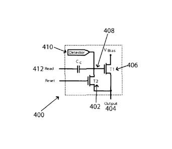
[0063] Another embodiment of the present invention is illustrated in figure
4.a. where
two-transistor multimode pixel sensor architecture 400 has been disclosed. As
shown in
Figure 4.b, the pixel sensor 400 can be reset to zero volts by turning on
transistor T2 402
and grounding the output 404. This ensures that the gate of transistor Ti 406
stays at zero
volts, or below, during integration which makes most of the operation time of
the array.
Sub-threshold voltages at the gate 408 of Ti 406 will not cause any threshold
voltage
CA 02639498 2008-09-11
MBM File: 1308-108
increase of Ti 406. The preset voltage changes depending upon amount of charge
received from the detector 410 during integration time. To read the pixel
value in APS
mode, a positive voltage pulse is applied to the read line 412. Because the
charge gate
408 is floating during the read (T2 402 is OFF, and the detector is ultra high
resistive), Ti
406 behaves like a charge gated transistor, therefore, depending on the read
voltage level
(at 412), pixel biasing voltage (at 416) and geometric design of Ti 406 and
capacitor Cc
418, Ti 406 is biased either in saturation or in linear mode, so that the
output current (at
404) is determined by equation 4 or 6, respectively, as previously explained.
[0064] Figure 4.c illustrates array configuration 420 of the multimode 2T
(two-
transistor) pixel architecture according to an embodiment of the present
invention. It is
worth noting that pixel biasing voltage VBIca, could be a global voltage
source or provided
separately for each row of the array. The array 420 can be read in C-APS or
PPS modes
using the multimode output column circuit shown in figure 4.d, and signal
waveforms
illustrated in figures 4.e and 4.f respectively. In either case, the array is
entirely reset at
first, 461, as illustrated in figures 4.e. and 4.f., and rows 426a, 426b, and
426c are
successively scanned after exposure 462. Vrst 452 is pulsed 463 to discharge
Cf 454 and
reset the output voltage Vout 456 before reading the next row. In one
embodiment, Vcnt
455 may be grounded, and Vout may be the voltage across capacitor Cf, which is
reset to
zero volts during the reset operation. Use of current sink 457 is optional,
with both Vbg
and Vbd negative. Using the two sample & hold circuits 458 and 459 shown in
figure 4.d,
double sampling can be performed to remove fixed pattern noises (FPN) and also
to
correct for nonuniformities in pixel characteristics across the large area
array.
[0065] As an alternative to current integrators, transimpedance amplifiers
485 can be
used in column circuit 480 as illustrated in figure 4.g, where the output
current of the
addressed pixel is immediately converted to an equivalent voltage without time
consuming integration operation; same waveforms 460 of figure 4.e (without
Vrst) are
used. Use of current sink 487 is optional. The array can also be read in V-APS
mode if
the output circuit 490 of figure 4.h is connected to each column, and
waveforms 460 of
figure 4.e (without Vrst) are used. This circuit uses a voltage amplifier 496,
and output
16
CA 02639498 2008-09-11
MBM File 1308-108
load 497 is optional. As the waveforms of figure 4.i show, real time scanning
of the array
is possible when each row is first read 492a, 492b and then reset 493a, 493b,
however,
because the pixel is reset and read via the same output line 494, the required
scanning
time for each row, At 495, is at least equal to the sum of resetting and
reading times,
which makes the frame rate long using this 2T multimode architecture. Signal
waveforms
of figure 4.e can also be adapted for operation of the circuit of figure 4.h.
While the read
time can be shortened at the price of pixel output gain, the resetting time
remains the
limiting factor for how fast an array can be scanned.
[0066] In
contrast with the architecture presented in figure 4.a where the pixel sensor
is reset through the output line, figure 5.a illustrates two-transistor pixel
sensor
architecture 500 with independent reset 502 as another embodiment of the
present
invention. As shown in figure 5.b, driving signals 512, 514 for this
architecture are
similar to the multimode 2T architecture, in addition to the fact that there
is no need to
ground the output line 504 while pixels are being reset. Therefore it is
possible to read
one row of the sensor array, while resetting the others. This provides the
opportunity to
read a high gain APS array much faster than a PPS array with similar image
quality.
Array configuration 520 of this two transistor active pixel architecture is
demonstrated in
figure 5.c. Current mode or voltage mode outputs could be used if column
circuits of
figures 4.d 450, 4.g 480, and 4.h 490 are connected to the output lines 594 or
output 504
in the case of a single pixel. In one embodiment, signal waveforms presented
in figure
4.e can be adapted for operation of the circuit in this case. As signal
waveforms of figure
5.d show, instead of resetting one line at a time, multiple lines are reset
532, 534 at a
fraction of the same time, and one line is read 536, 538 at the very time. For
example, a
charge gain of 15 drops to 3 if the readout time (and so the resetting time)
is decreased
five times, from 30p.s to 61..ts. Now instead of resetting each row for 30 s,
5 rows are
simultaneously reset for only 6[1s, and the whole resetting window and the row
being
read sweep the array 520 at the speed of one row per 61.is (instead of one row
per ¨30[ts);
five times higher frame rate. In one embodiment, high pixel gain makes it
possible to
reduce readout time, and multiple rows are independently reset which can
reduce At.
17
CA 02639498 2016-09-06
[0067] Another embodiment of the present invention is single transistor
active pixel
architecture 600 as depicted in figure 6.a. Low voltage detectors 602 such as
pin diodes
are assumed to be used for this architecture, so that, the pixel sensor is
reset by applying a
proper bias voltage (at 604) to bias the detector diode in the forward mode.
The detector
bias voltage (at 604) is then reduced to slightly negative voltages for proper
operation of
the detector diode 602, an also to make sure that the amplifying transistor,
Ti 606, is in
OFF state. Reading the pixel value is performed as previously explained for 2T-
APS
architectures (refer to figure 6.b for different cycles of operation of single
transistor APS
architecture). The array configuration 610 of the architecture is illustrated
in figure 6.c,
where the outputs can be read 612 in current or voltage mode depending on the
type of
readout circuit connected to the columns (circuits illustrated in figures 4.d
450, 4.g 480,
and 4.h 490 could be used for C-APS or V-APS operation modes). By applying
signal
waveforms 620 of figure 6.d, the array 610 could be used for single shot
scanning, while
signals 630 of figure 6.e can be used for real time scanning.
[0068] The embodiments of the invention being thus described, it will be
obvious that
the same may be varied in many ways. Such variations are not to be regarded as
a
departure from the scope of the invention, and all such modifications as would
be
obvious to one skilled in the art are intended to be included within the scope
of the
following claims.
18