Note: Descriptions are shown in the official language in which they were submitted.
CA 02640455 2008-07-25
WO 2007/091937 PCT/SE2006/050263
1
LAMINATE STRUCTURE AND METHOD OF PRODUCING THE SAME
Field of invention
The invention relates to a laminate structure
comprising a first carrier layer with a surface, a first
active surface being electrically conducting and being
supported by the first carrier layer, a second active
surface being electrically conducting and being supported
by the first carrier layer.
The invention further relates to a method of
producing such a laminate structure.
Technical Background
The old way of distributing products in large
distribution packages, followed by repacking of the
products behind the store counter in paper bags, or the
like, in the amount as bought by the consumer, has almost
completely disappeared. Decades ago the wide spread of
the large self service stores, with pre-packed products
stored on shelves, from which the consumers themselves
pick the products, lead to great developments in the
packaging industry.
Today almost all consumer products are packed at the
manufacturing or processing site, distributed, sold, and
often also stored in the consumers home, in one and the
same package. One popular kind of package used for almost
all kind of products is a box made of paperboard.
Paperboard boxes are, e.g., widely used for dry food
products and for small commodity items such as screws and
nails. By providing an inner bag the paperboard box may
also be used for liquids or for powder products, such as
cocoa or dry milk. This kind of package is also widely
used for cereals and similar products.
This kind of package is often adapted to be opened
by first tearing off a tearing band or strip from the
CA 02640455 2008-07-25
WO 2007/091937 PCT/SE2006/050263
2
paperboard box and then cutting (with a pair of scissors)
the inner bag open. The tearing band often extends across
the complete top surface, from side edge to side edge,
and separates a front flap connected with the front side
of the container from a rear flap connected to the back
side of the package. The front and rear flaps are often
spot glued to side flaps folded from the sides of the
package underneath the front and rear flaps. When the
consumer opens such a package the tear band often breaks
and the tearing action need to be restarted again.
Moreover, the tear band often does not separate from the
flaps as intended, which makes it more difficult to open
the package and which often results in that any reclosing
means, such as flaps and slits, are damaged.
Another kind of package often used as a consumer
package is a bottle or jar formed of plastic or glass
provided with a screw cap or snap lid formed of plastic
or metal. This kind of package has an intrinsic problem
relating to the compromise of providing a sufficiently
low initial opening force and a sufficiently good
sealing. Most caps or lids on this kind of package are
fastened by threads or bayonet mount. In order to provide
the necessary sealing pressure, the caps or lids must be
fastened with a significant torque. Within the packaging
industry there exist numerous variants concerning how to
avoid the need for application of a high torque for
closing the package. However, as will be discussed below,
these variants introduce different drawbacks for the
consumers when opening the packages, and especially at
initial opening of the packages.
One kind of package often used for jam, pickled
gherkin, and the like is a glass jar with a metal lid.
Such a package is often filled by hot-filling or the like
in order to create a negative pressure inside the jar.
This negative pressure will force the lid against the
mouth of the jar and will thereby improve the quality of
the sealing between the lid and jar. However, this way of
CA 02640455 2008-07-25
WO 2007/091937 PCT/SE2006/050263
3
creating a good seal has the drawback that it is very
hard to open such a jar; when trying to rotate the lid,
the negative pressure will give rise to a high friction
force counteracting the intended opening action. This
kind of package also requires that the jar and lid are
formed of relatively rigid components in order to be able
to withstand the forces involved.
One kind of package often used for dry products,
such as instant coffee, is a glass jar with a simple
plastic lid. In order to provide sufficient sealing, the
jar is, underneath the lid, provided with a sealing film
or membrane. Such a sealing membrane is often also
provided on plastic bottles for ketchup, mustard or the
like, and boxes for table margarine or the like, where
the lid has a snap functionality or some other
functionality which is difficult to use to provide a
sealing action. The film or membrane is often glued or
fused to the mouth of the package. However, this kind of
package suffers from the drawback that the necessary
tearing off force must be sufficiently low for the user
to be able to tear off the membrane and preferably in one
piece, but the membrane should also be securely sealed to
the mouth and it should from cost and environment aspects
be as thin as possible. The result is often that the
consumer has difficulties in tearing off the membrane at
all or in tearing off the membrane in one piece. The
membrane is only partially torn off, it is often
difficult to get rid of the remainders since any grip tab
or the like has already been torn off.
Thus, the known packages all suffer from different
drawbacks when it comes to opening of the packages.
Common for all kinds of consumer packages is that
they contain consumer adapted volumes or amounts of the
product in question. This gives that the consumer
packages each have a relatively small volume compared to
the total volume sold by each store and even smaller
compared to the total volume distributed to a number of
CA 02640455 2008-07-25
WO 2007/091937 PCT/SE2006/050263
4
stores in the same distribution area. It is not practical
for the store or distribution personnel to handle every
single consumer package one by one. This is one major
reason for the wide spread use of distribution packages
housing several consumer packages.
One commonly used distribution package is a
corrugated cardboard box enclosing the consumer packages.
The corrugated cardboard is usually folded to form an
open ended box, filled with the consumer packages and
closed by gluing together two or more flaps. In automatic
processes it is also common to gather several consumer
packages side by side and then the corrugated cardboard
box is formed by basically wrapping the cardboard about
the consumer packages and finally close it by gluing
together one or more flaps. Cardboard boxes are usually
opened by either cutting the cardboard using a knife,
tearing the glued flaps open by hand, or tearing the
cardboard along perforations by hand. Using a knife
introduces the risk of personnel injuries or damages to
the consumer packages. In order to avoid handling the
consumer packages one by one, it is often also desirable
to be able to keep a part of the distribution package as
a bottom tray or the like, making it possible to put
several consumer packages onto the shelf in one heave.
Such a package is usually designed to be opened by a
tearing action. However, the cardboard box is often torn
apart instead of simply torn open, when the store
personnel tears the glued flap open or tears the
cardboard along any perforation. This is not satisfactory
since it will give an impression of low quality
reflecting negatively on the product and the store. Since
the tray usually need to be provided with a rim, i.e. a
lower portion of the side walls need to be left, in order
to provide the necessary stability, it is difficult to
open such a distribution package using a knife without
damaging the consumer packages. The cardboard box may
alternatively be closed using interlocking flaps.
CA 02640455 2008-07-25
WO 2007/091937 PCT/SE2006/050263
However, it is often hard to accomplish an automatic
closing of such a box. Moreover, the flaps often need to
be removed by a tearing or cutting action when the box is
to be put on the store shelf. Thus this kind of box is
5 also associated with the problems relating to tearing or
cutting of the cardboard as discussed above.
A simple and cheap way of providing a distribution
package is to plastic film wrapping several consumer
packages. This requires however often that the consumer
packages as such are relatively form stable. When the
consumer packages are to be put on the store shelves, the
store personnel cuts the film wrapping open, using a
knife, and put the consumer packages one by one on the
shelf. The use of a knife introduces the risk of
personnel injuries or damages to the consumer packages.
Moreover, the store personnel still has to handle the
consumer packages one by one. By putting the consumer
packages on a tray and then film wrap the tray together
with the consumer packages, this one by one handling may
be avoid. This kind of distribution package is often used
for metal cans, plastic bottles and plastic tubes
distributed standing up on the tray. However, the film
wrapping still has to be cut open.
Consumer packages and distribution packages have
been used wide spread for several decades within almost
every line of business but as has been discussed above
the different kind of distribution packages are all
associated with different problems.
Summary of invention
It is an object of the invention to provide a
laminate structure which may be used to eliminate or at
least to reduce the above mentioned problems. The
inventive laminate structure may be used in other
applications than the ones discussed above and in the
detailed description.
CA 02640455 2008-07-25
WO 2007/091937 PCT/SE2006/050263
6
The above objective has been achieved with a
laminate structure comprising a first carrier layer with
a surface, a first active surface being electrically
conducting and being supported by the first carrier
layer, a second active surface being electrically
conducting and being supported by the first carrier
layer, wherein the first active surface is separated from
the second active surface a first distance along the
surface of the first carrier layer, wherein the laminate
structure is adapted to receive an electrically weakable
adhesive bridging said distance between the active
surfaces.
In this way, it is possible to pre-manufacture parts
of the structure with the active surfaces on a carrier
layer. When applying the laminate structure to a package
or to a connecting element a number of advantages are
achieved.
It may be noted that supported does not necessarily
mean that the active surfaces need to be in direct
contact with the first carrier layer. In one embodiment
the first active surface is laminated directly onto the
first carrier layer, whereas significant portions of the
second active surface is laminated onto an insulating
layer laminated onto the first active surface. The
laminate structure is still supported by the first
carrier layer.
As mentioned above, glued cardboard packages are
today often provided with a tear strip. By using the
inventive laminate structure it is possible to introduce
a new design of the package, whereby there is no longer
any need for such a tear strip. The package is glued
together at filling of the package using an electrically
weakable adhesive. When the consumer would like to open
the package, a voltage is applied to the electrically
weakable adhesive and the adhesive looses its adhesive
force. The package is thereafter easily opened without
any risk of being incorrectly torn open and without any
CA 02640455 2008-07-25
WO 2007/091937 PCT/SE2006/050263
7
risk of damaging any reclosure tabs/slots or the like.
The package with inventive laminate structure and the
electrically weakable adhesive may also be designed or
configured in a manner not possible today. When designing
a conventional package, the designer must balance design
requirements relating to erecting and closing of the
container with design requirements relating to opening of
the container. This often results in that the closing of
the container is unnecessary complicated and still it is
hard to open the container as intended. This problem is
eliminated or at least greatly reduced with a package
using the inventive laminate structure. It is e.g.
possible to design the container in a way that gives a
simple erecting and closing of the container by simply
using adhesive connections where connection is desired.
When the user wants to open the package a voltage is
applied to the electrically weakable adhesive, and the
desired connections are easily released. In this way it
is further possible to design the package to be as strong
as possible without the need for any far-reaching
compromises concerning how to still make opening of the
package easy. The package is in any case simply opened by
the application of a voltage to the electrically weakable
adhesive.
Similarly, for a package with a body and a cap the
introduction of the inventive laminate structure makes it
possible to provide a package which is tightly closed in
distribution and which still is easily opened. The
laminate structure with the electrically weakable
adhesive may, e.g., be used to secure a screw cap from
unintentionally being screwed of the bottle and, after
being subjected to a voltage, still easily release the
cap from the bottle when the package is to be opened.
This may also be used for a foil covered opening. The
foil is securely fastened to the mouth of the bottle or
jar by forming part of the inventive laminate structure
with the electrically weakable adhesive. When the package
CA 02640455 2008-07-25
WO 2007/091937 PCT/SE2006/050263
8
is to be opened, a voltage is applied and the foil is
easily removed. Thereby it is possible to even fasten the
foil so securely that it is impossible to tear it off
without applying a voltage. In any case it is possible to
secure the foil to a greater extent than today and still
make it possible to release it much easier than today.
With this difference in securing power it is possible to
design very thin foils, since they after application of a
voltage only have to withstand any remaining tear-off
resistance instead of as today where they during tear-off
have to withstand the original tear-off resistance being
designed to be high enough to keep the foil secured to
the package during distribution.
The use of the inventive laminate structure with a
electrically weakable adhesives also allows for the
application of a tamper-proof feature integrally formed
with the initial closure of the package. When the
electrically weakable adhesive has reacted, it will no
longer return to the same strong adhesive strength and it
will thereby provide a tamper-proof feature.
The voltage applied may be either alternating or
direct depending upon the desired manner of weakening of
the electrically weakable adhesive. The voltage may e.g.
be applied by an external source, such as a battery, by
electromagnetic waves, or by designing the package with
active surfaces of different materials with different
electrode potentials, thereby forming an internal
battery.
The inventive laminate structure may also be used in
a connecting element provided with adhesion areas
comprising an electrically weakable adhesive. With this
connecting element it is possible to provide new kinds of
distribution solutions. The connecting element may be
used to hold together packages or other kinds of products
and articles.
It may e.g. be formed as board shaped members
arranged beneath or on top of a pallet of packages. By
CA 02640455 2008-07-25
WO 2007/091937 PCT/SE2006/050263
9
holding the packages to the connecting element, the set
of packages and connecting element will form a
distribution unit with improved handleability. When the
shop assistant has placed the distribution unit in place
on the display shelf, the packages are easily released by
application of voltage to the electrically weakable
adhesive. Since there is no need for any tearing or
cutting of any distribution package, there is no need for
any additional space between the products or packages and
the surrounding display shelves. In accordance with one
embodiment the shop assistant simply slides a set of
eight packages from the pile of product on the pallet
lifter to the display shelf, the packages being held
together by an underlay and a top board. Thereafter the
assistant activates the internal battery applying a
voltage to the adhesion areas with the electrically
weakable adhesive and thereby releasing the top board
from the packages. The assistant withdraws the top board
from the display shelf and finalises the loading of the
shelf with activation of the internal battery of the
underlay, thereby releasing the packages also from the
underlay. When the consumer picks the packages from the
shelf they are easily picked from the shelf and underlay
since they are already released from the underlay. It is
also contemplated that in some cases the packages are
released from the connecting element used during
distribution and then put one by one on the display
shelf.
The inventive laminate structure may also be used in
a package comprising a first adhesion area by which
adhesion area said package is adapted to be temporarily
connected to one or more other packages, wherein the
adhesion area comprises an electrically weakable
adhesive. A set of packages are held together during
distribution by one or more packages provided with the
electrically weakable adhesive. Numerous variations
concerning when to release the packages are contemplated.
CA 02640455 2008-07-25
WO 2007/091937 PCT/SE2006/050263
The shop assistant lifts the set of packages to the
display shelf and then releases them to leave them
arranged together but released from each other. In this
way it will be possible to make use of the distribution
5 solution for the shop assistant whereas the consumer does
not notice any difference compared to the solution of
today. It is also contemplated to release them and then
putting them one by one on the shelf. This is suitable if
the packages are to heavy or bulky to handle in sets of
10 packages. It is also contemplated that the packages are
released from the neighbouring packages by the consumer
when lifting them from the shelf. This gives information
to the consumer that this package has not been released
before. This is e.g. useful for cooled or frozen
products; if you have to release it you know that no
other consumer has walked around in the store with the
product in the shopping cart and then changed his or her
mind and put it back in the freezer. It is also
contemplated that the packages are bundled together and
sold together and only separated when the consumer puts
the products in the cabinets at home or even when he or
she is about to open the package. This may e.g. be used
for selling a primary product and one or more associated
products, such as pasta and pasta sauce, as a bundled
package.
The inventive laminate structure may also be used in
an article forming a handling element comprising a first
adhesion area, adapted to temporarily holding at least
one secondary article to said handling element, and an
engagement area by which the handling element and the
secondary article connected thereto are adapted to be
handled, wherein the adhesion area comprises an
electrically weakable adhesive. Such a design is e.g.
useful for handling and displaying consumer articles on a
rack. It may e.g. be used to display pencils or similar
products that today are put behind a plastic cover on a
CA 02640455 2008-07-25
WO 2007/091937 PCT/SE2006/050263
11
paper board. The electrically weakable adhesive may be
used to connect the article directly to the paper board.
It may be noted that most of the advantages has been
discussed in respect of the complete product comprising
the first and the second carrier layer and the
electrically weakable adhesive. As mentioned initially
one advantage of the inventive laminate structure is that
it is possible to pre-manufacture the laminate structure
in different steps and at different locations. The
carrier layer may, e.g., be manufactured at a first
location and then afterwards be provided with the active
surfaces. The active surfaces may be provided using a
printing technique where conductive ink is applied to the
carrier layer. The active surfaces may also be formed of
conductive foils laminated as foils or as molten
materials to the carrier layer. Such a laminate structure
may then be stored or distributed as a unit. It may also
form part of a package or some other final product. The
electrically weakable adhesive may then as a separate
step be provided to the laminate structure when the
intended products or portions of a product is to be
connected to each other. Other variants of this
possibility to pre-manufacture the laminate structure in
different levels from the carrier layer to the complete
laminate structure will follow from the description of
preferred embodiments.
Preferred embodiments of the invention appear from
the dependent claims.
The first carrier layer may be formed of a non-
conductive material. In this way the conductors may
simply be provided as printed or laminated conductors on
the non-conductive material. There will be no immediate
need for more complicated laminate structures with
insulating layers, etc.
The first carrier layer may be formed of paper
board. This material is preferred since it is easy to
provide a connecting element or package in paper board.
CA 02640455 2008-07-25
WO 2007/091937 PCT/SE2006/050263
12
It is also normally non-conducting making it easy to
provide it with an electrical circuitry using e.g. a
printing or laminating technique.
The laminate structure may comprise an internal
source of electrical power adapted to be activated or
connected to the active surfaces to in a closed
electrical circuit apply a voltage to the electrically
weakable adhesive. In this way the package or connecting
element may be released anywhere and by anyone. This is
especially useful for solutions where the packages are
released by the consumer when he or she picks them from
the shelf and for solutions where bundled packages are to
be released after being purchased.
The first active surface may be of a first material
with a first electrode potential, and the second active
surface may be of a second material with a second
electrode potential, and wherein the first electrode
potential differs from the second electrode potential. In
this way, the active surfaces as such will act as an
internal electrical source and will when connected to
each other via a electrical circuitry outside the
electrically weakable adhesive form a closed electrical
circuit applying a potential difference across the
electrically weakable adhesive.
The laminate structure may further comprise at least
one printed and/or laminated battery. This is an
expedient way of providing an internal source of
electrical power.
The at least one printed and/or laminated battery
may be printed on a first carrier layer. This is an
expedient way of providing a battery forming an internal
source of electrical power. As indicated below the first
carrier layer may also be used to carry on or more active
surfaces. Thereby it is easy to provide a connection
between the battery and the one or more active surfaces
on the first carrier layer.
CA 02640455 2008-07-25
WO 2007/091937 PCT/SE2006/050263
13
A portion of at least one of said active surfaces
may be exposed and adapted to be covered by said
adhesive. In this way the electrically weakable adhesive
will in itself provide the conductive bridge to this
active surface.
At least a portion of the first active surface and
at least a portion of the second active surface may be
exposed and adapted to be covered by said adhesive. In
this way the electrically weakable adhesive will in
itself provide the conductive bridge to both active
surfaces.
The active surfaces may be shaped such that a
projection of the first active surface on the surface of
the first carrier layer essentially surrounds a
projection of the second active surface on the surface of
the first carrier layer. In this way the area in which
the electrically weakable adhesive will be broken or
weakened will be relatively large compared to the size of
the active surfaces. In this way the energy losses due to
resistance in the active surfaces will be minimized. It
will furthermore provide a rather concentrated weakening
of the adhesive, which will facilitate the opening of the
package.
A projection of the first active surface on the
surface of the first carrier layer and a projection of
the second active surface on the surface of the first
carrier layer may at least partly overlap each other,
wherein the laminate structure further comprises an
insulating layer provided between the first and second
active surfaces, at least at the overlap. By providing
active surfaces with overlaps and insulating layers there
between it is possible to optimise the shape of the
electrically weakened area, without having to be limited
by separation in the plane of the carrier layer.
The first active surface may be formed as a closed
loop with its projection on the surface of the first
carrier layer surrounding the projection of the second
CA 02640455 2008-07-25
WO 2007/091937 PCT/SE2006/050263
14
active surface on the surface of the first carrier layer,
wherein the second active surface has a connecting
portion extending out of the closed loop of the first
active surface, and wherein the electrically insulating
layer separates the connecting portion of the second
active surface from the first active surface. In this way
the electrical potential will be bridged by the
electrically weakable adhesive to the first active
surface all the way around the second active surface.
This will give a relatively large weakened area compared
to the size of the second active surface.
The laminate structure may further comprise an
electrically weakable adhesive bridging said distance
between the first and second active surfaces, and being
adapted to be located between the active surfaces and a
second carrier layer. It may e.g. be noted that the
laminated structure may be sold to a producer of a
complete product or package, the laminated structure
being provided with active surfaces but without any
electrically weakable adhesive thereon. The electrically
weakable adhesive may then be applied when the package is
to be closed or an article is to be connected to another
using the laminated structure with the electrically
weakable adhesive.
The laminate structure may further comprise a non
electrically weakable adhesive arranged as a layer
adapted to be located between the electrically weakable
adhesive and a second carrier layer. In this way it is
possible to pre-manufacture the structure with active
surfaces and electrically weakable adhesive and then to
apply a conventional adhesive on top of this when e.g.
the package is closed for the first time. When the
package is to be opened the electrically weakable
adhesive is weakened and the conventional adhesive will
be released together with the portion or package member
not carrying the active surfaces. It is also contemplated
to provide two layers of electrically weakable adhesive,
CA 02640455 2008-07-25
WO 2007/091937 PCT/SE2006/050263
one layer in the pre-manufacturing step and a second
layer when e.g. the package is to be closed.
The laminate structure may further comprise a second
carrier layer adhered to the first carrier layer and the
5 active surfaces by said electrically weakable adhesive or
said non electrically weakable adhesive.
The first carrier layer may form part of a first
portion of a package and the second carrier layer may
form part of a second portion of a package, wherein the
10 first and second portions of the package is adapted to be
connected to each other and thereby keep the package
closed.
The first carrier layer may form part of a first
package member and the second carrier layer may form part
15 of a second package member, wherein the first and second
package members are adapted to co-operate with each other
and thereby form a closed package.
The electrically weakable adhesive may form a
sealing layer. In this way it is possible to e.g. form a
securely sealed package which still may be easily opened.
The laminate structure may also provide a connecting
element wherein the first carrier layer forms part of the
connecting element adapted to temporarily holding
together a plurality of articles, the connecting element
comprising a base member provided with a first adhesion
area adapted to hold a first secondary article to said
base member and a second adhesion area adapted to hold a
second secondary article to said base member, wherein the
adhesion areas comprise an inventive laminate structure.
With this connecting element it is possible to provide
new kinds of distribution solutions. The connecting
element may be used to hold together packages or other
kinds of products and articles. The advantages and
different embodiments of such a connecting element has
been discussed in more detail above with respect to
different manners of making use of the inventive laminate
structure.
CA 02640455 2008-07-25
WO 2007/091937 PCT/SE2006/050263
16
The above disclosed laminated structure may also be
used to provide an article forming a handling element
comprising a first adhesion area, adapted to temporarily
holding at least one secondary article to said handling
element, and an engagement area by which the handling
element and the secondary article connected thereto are
adapted to be handled, wherein the adhesion area
comprises an electrically weakable adhesive. Such a
design is, e.g., useful for handling and displaying
consumer articles on a rack. It may e.g. be used to
display pencils or similar products that today are put
behind a plastic cover on a paper board. The electrically
weakable adhesive may be used to connect the article
directly to the paper board.
The above objective has also been achieved by a method of
producing a laminate structure, the method comprising
providing a first carrier layer,providing a first active
surface being electrically conducting and being supported
by the first carrier layer, providing a second active
surface being electrically conducting, supported by the
first carrier layer and separated from the first active
surface a first distance along the surface of the first
carrier layer, and providing a layer of an electrically
weakable adhesive at least partly bridging said distance
between the first and second active surfaces.
It may be noted that most of the advantages has been
discussed in respect of the complete product comprising
the first and the second carrier layer and the
electrically weakable adhesive. As mentioned initially
one advantage of the inventive laminate structure is that
it is possible to pre-manufacture the laminate structure
in different steps and at different locations. This is
disclosed by the inventive method.
The carrier layer may e.g. be manufactured at a
first location and then afterwards be provided with the
active surfaces. The active surfaces may be provided
using a printing technique where conductive ink is
CA 02640455 2008-07-25
WO 2007/091937 PCT/SE2006/050263
17
applied to the carrier layer. The active surfaces may
also be formed of conductive foils laminated as foils or
as molten materials to the carrier layer. Such a laminate
structure may then be stored or distributed as a unit. It
may also form part of a package or some other final
product. The electrically weakable adhesive may then as a
separate step be provided to the laminate structure when
the intended products or portions of a product is to be
connected to each other. Other variants of this
possibility to pre-manufacture the laminate structure in
different levels from the carrier layer to the complete
laminate structure will follow from the description of
preferred embodiments.
Preferred embodiments of the invention follows from
the dependent claims.
The method may further comprise providing an
electrically weakable adhesive onto the laminate
structure such that it bridges said distance between the
active surfaces. As mentioned above the electrically
weakable adhesive may then as a separate step be provided
to the laminate structure when the intended products or
portions of a product is to be connected to each other.
The advantages of respective feature of the
dependent claims has been discussed in detail with
respect to the corresponding features of the dependent
claims relating to the laminate structure and will not be
repeated with respect to the preferred embodiments of the
method. Reference is made to the detailed discussion
above.
A portion of at least one of said active surfaces
may be exposed and wherein the adhesive is provided onto
the laminate structure such that it covers said portion.
At least a portion of the first active surface and
at least a portion of the second active surface may be
exposed and wherein the adhesive may be provided onto the
laminate structure such that it covers said portions.
CA 02640455 2008-07-25
WO 2007/091937 PCT/SE2006/050263
18
The active surfaces may connectable to each other
via an electrical circuit comprising a switch member by
which the circuit may be closed or opened. This is a
simple way of providing a way of in a controlled manner
apply a voltage to the electrically weakable adhesive.
The active surfaces may be provided such that a
projection of the first active surface on the surface of
the first carrier layer essentially surrounds a
projection of the second active surface on the surface of
the first carrier layer.
The active surfaces may be provided such that a
projection of the first active surface on the surface of
the first carrier layer and a projection of the second
active surface on the surface of the first carrier layer
at least partly overlap each other,
wherein the method further comprising providing an
insulating layer between the first and second active
surfaces, at least at the overlap.
The first active surface may be provided such that
it forms a closed loop with its projection on the surface
of the first carrier layer surrounding the projection of
the second active surface on the surface of the first
carrier layer, wherein the second active surface may be
provided with a connecting portion extending out of the
closed loop of the first active surface, and wherein the
electrically insulating layer may separate the connecting
portion of the second active surface from the first
active surface.
The method may further comprise providing a non
electrically weakable adhesive as a layer between the
electrically weakable adhesive and a second carrier
layer.
The method may further comprise the step fo
providing a second carrier layer adhered to the first
carrier layer and the active surfaces by said
electrically weakable adhesive or said non electrically
weakable adhesive.
CA 02640455 2008-07-25
WO 2007/091937 PCT/SE2006/050263
19
The method may further comprise the step of
providing the first carrier layer as a part of a first
portion of a package and providing the second carrier
layer as a part of a second portion of a package, wherein
the first and second portions of the package is adapted
to be connected to each other and thereby keep the
package closed.
The method may further comprise the step of
providing the first carrier layer as a part of a first
package member and providing the second carrier layer as
a part of a second package member, wherein the first and
second package members are adapted to co-operate with
each other and thereby form a closed package.
The electrically weakable adhesive may form a
sealing layer.
The method may further comprise providing the first
carrier layer as a part of a connecting element adapted
to temporarily holding together a plurality of articles,
the connecting element comprising a base member provided
with a first adhesion area adapted to hold a first
secondary article to said base member and a second
adhesion area adapted to hold a second secondary article
to said base member, wherein the adhesion areas comprise
an inventive laminate structure as disclosed in detail
above.
Brief description of the drawings
The invention will by way of example be described in
more detail with reference to the appended schematic
drawings, which shows presently preferred embodiments of
the invention.
Fig 1 shows in an exploded view a first embodiment
of a basic structure in accordance with the invention
with the active surfaces arranged on the same side of the
adhesive layer.
CA 02640455 2008-07-25
WO 2007/091937 PCT/SE2006/050263
Fig 2 shows in an exploded view a second embodiment
of the basic structure of fig 1.
Fig 3 shows a cross-section of the structure in
fig 2.
5 Fig 4 shows in an exploded view of a third
embodiment of the basic structure of fig 1.
Fig 5 shows an embodiment where twelve packages are
being held together by two panels.
Fig 6-8 indicate three different alternatives of how
10 an electrical energy may be applied in order to weaken
the adhesive.
Fig 6 shows a first embodiment of a panel as shown
in fig 5.
Fig 7 shows a second embodiment of a panel as the
15 one shown in fig 5.
Fig 8 shows a third embodiment of a panel as the one
shown in fig 5.
Fig 9 shows three packages held together to form a
distribution unit.
20 Fig 10a shows two packages of the kind shown in
fig 9 after they have been separated from each other.
Fig 10b shows in enlargement a portion of the
package of fig 10a.
Fig lla shows in cross-section a package.
Fig llb shows in cross-section the package of
fig lla when opened.
Fig 12 shows a portion of a bottle neck provided
with a screw cap.
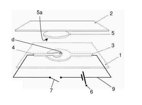
Detailed description of preferred embodiments
The basic structure comprises a first carrier layer
1 and a second carrier layer 2. A first active layer 3 is
laminated on the first carrier layer 1. A second active
layer 4 is laminated on the second carrier layer 2. The
active layers are bonded together by a bonding layer 5,
which bonding layer comprises an electrically weakable
adhesive.
CA 02640455 2008-07-25
WO 2007/091937 PCT/SE2006/050263
21
The electrically weakable adhesive may bridge the
complete distance between the active layers but may also
be completed with additional layers of other materials
capable of performing the necessary electrical and/or
mechanical connection. Such materials may be conventional
non electrically conductive adhesives, polymers,
varnishes, or the like, or electrically conductive
versions of respective material.
Fig 1-4 show embodiments wherein the active surfaces
are arranged on the same side on a first carrier layer.
In fig 1, 2 and 4, the different layers are for clarity
reasons illustrated at a distance from each other.
However, it is apparent that in practice the layers forms
a laminated structure. From the description below it will
follow in which cases the different disclosed layers need
to be in direct contact with each other and when there
may be one or more additional, non-disclosed layers
between the disclosed layers. It may also be noted that
in direct contact may dependent upon the situation mean
in mechanical contact or in electrical contact.
Fig 6-8 shows a connecting element with three
different alternatives of how to apply the electrical
energy to break or weaken the bond of the bonding layer.
In fig 6 and in fig 1-4, the electrical potential
difference between the active layers 3, 4 is adapted to
be provided by an external source 6 of electrical energy
(indicated by the + and - signs). This external source
may e.g. be a battery provided in a handheld device, or a
battery being attached to the package and connectable to
the active layers 3, 4. One or several batteries can,
e.g., be printed on one of the carrier layer and
connected to the active surfaces. In this design the two
active layers 3, 4 may, but need not, be formed of the
same material. When a voltage is applied between the
active surfaces 3, 4, current will flow between the
active surfaces 3, 4 via the bonding layer 5. This will
cause the bonds in the bonding layer 5 or between the
CA 02640455 2008-07-25
WO 2007/091937 PCT/SE2006/050263
22
bonding layer 5 and one or both of the active surfaces 3,
4 to break or to weaken. The current applied may be in
the form of direct current or alternating current. A
direct current is preferably used to weaken the bonds in
the bonding layer 5 or between one of the active surfaces
3 or 4 and the bonding layer 5. An alternating current is
preferably used to weaken the bonds in the bonding layer
5 or between both of the active layers 3, 4 and the
bonding layer 5.
In fig 7, the electrical potential difference
between the active layers 3, 4 is adapted to be provided
by making the active layers 3, 4 of different materials
with different electrode potentials. If the two active
layers 3, 4 are connected, e.g. by moving a switch 7 to a
position where it connects the two layers 3, 4, a closed
circuit is formed and current will flow through the
bonding layer 5, thereby causing the adhesive bond to
break or weaken. For example, copper and graphite can be
used as active layers 3, 4 with different potentials.
This design will create a flow of direct current between
the active layers 3, 4 via the bonding layer 5.
In fig 8, the electrical potential difference
between the active layers 3, 4 is provided by supplying
electro magnetic waves, e.g. radio waves, to the package.
The active layers 3, 4 or a separate member 8 connected
to the active layers 3, 4 may be adapted to be subjected
to the electro magnetic waves and transform this wave to
an electrical potential difference between the active
layers 3, 4. The AC voltage generated by the electro
magnetic waves can be can be used directly or transformed
to DC voltage by a rectifier, e.g. a half-wave rectifier
or a full-wave rectifier, connected to the active
surfaces.
This member 8 may, e.g., be an antenna or a coil. In
this design the two active layers 3, 4 may, but need not,
be formed of the same material.
CA 02640455 2008-07-25
WO 2007/091937 PCT/SE2006/050263
23
Although the discussion concerning the different
manners of providing the electrical potential difference
or voltage has referred to fig 6-8, the teachings may be
used in respect of the different applications of the
laminate structure as deemed suitable.
The use of controlled delaminating material in the
collation of products in transit or handling and
subsequent separation of the products, diminish the need
for extra material and facilitate the distribution of
products.
The connecting elements and packages described in
the following make use of an electrically weakable
adhesive material. The inventive connecting elements and
packages are provided with two active surfaces, being
electrically conducting and acting as electron and/or ion
emitter and receiver, connected with a bonding layer
formed by the electrically weakable adhesive material.
The bonding layer possesses adhesive properties and
conductive properties. When a voltage is applied between
the active surfaces and current flows through the bonding
layer, bonds formed in or between the bonding layer and
at least one of the active surfaces are broken or
weakened. Thus, the bonding layer forms an electrically
weakable adhesive.
The electrically weakable material and different
basic configurations of the active surfaces will
initially be discussed in detail separately from the
specific designs of the different uses. The different
uses will thereafter be discussed in detail. In some
cases the design of the package will be discussed in
combination with a specific kind of basic configuration.
It should however be noted that this is for exemplifying
purposes and that the different basic configurations may
be combined with the different designs of the packages.
According to one embodiment the bonding layer is
composed of a composition possessing both matrix
functionality and electrolyte functionality. The matrix
CA 02640455 2008-07-25
WO 2007/091937 PCT/SE2006/050263
24
and the electrolyte functionalities may be formed by a
single phase or several separate phases.
The matrix functionality provides the adhesive
properties necessary to bind surfaces to one another
mechanically or chemically. The matrix functionality may
be provided by polymers, polymer resins or fibres that
possess adhesive properties.
The electrolyte functionality provides the ion
conductivity necessary to support a faradic reaction,
i.e. an electrochemical reaction in which a material is
oxidized or reduced, or some other chemical/physical
reaction. The materials are preferably chosen and
designed such that the reaction occurs at the interface
between one or both of the active surfaces and the
bonding layer. Alternatively the bonding layer may be
designed such that the reaction will occur within the
bonding layer. This may, e.g., be accomplished by
providing islands of a material with electrolyte
functionality within the matrix material. The electrolyte
functionality may be provided by adding a salt to the
material or by modifying the polymer so that it includes
ion-coordinating moieties.
The electrically weakable adhesive used in the
inventive packages may be the electrochemically
disbondable composition ElectRelease TM supplied by EIC
laboratories and disclosed in more detail in
US 6,620,308.
Fig 1 shows an embodiment wherein the active
surfaces 3, 4 are arranged on the same side of the
bonding layer, which bonding layer comprises an
electrically weakable adhesive. The structure comprises
two carrier layers 1, 2 that are to be delaminated. The
carrier layers 1, 2 may, e.g., be made of paper, paper
board or plastic, but other materials are contemplated.
The active surfaces 3, 4 are arranged on one side of the
bonding layer 5 and are separated from each other a
distance d along the surface 5a of the carrier layer 1
CA 02640455 2008-07-25
WO 2007/091937 PCT/SE2006/050263
The active surfaces 3, 4 may be applied to the first
carrier layer 1 using any conventional method, they may
,e.g., be printed or laminated onto the carrier layer 1.
The active surfaces 3, 4 may be made of any conductive
5 material, e.g. metal ink or foil. The bonding layer 5 is
provided between respective active surface 3, 4 and the
second carrier layer 2, thereby bonding the active
surfaces 3, 4 to the second carrier layer 2 and in turn
thereby bonding the two carrier layers 1, 2 to each
10 other. The bonding layer 5 typically reaches the first
carrier layer 1 in the small accessible area formed by
the gap or distance d between the active surfaces 3, 4.
As shown in fig 2, one of the active surfaces 3 has an
area of distribution formed as an open half-circle
15 partially enclosing the other active surface 4. This
other active surface 4 has an area of distribution formed
as a circle. The two active surfaces 3, 4 form a gap
formed as a part of a ring, in this case a part of a
circular ring, having a width defined by the above
20 mentioned distance d. Other shapes, such as squares are
also contemplated.
The active surfaces 3, 4 are also connected or
connectable to each other via a circuit 9 comprising an
external power supply 6 and a switch 7.
25 When a voltage is applied between the active
surfaces 3, 4, e.g. by the closure of the switch 7,
current will flow between the active surfaces 3, 4 via
the bonding layer 5. This will cause the bonds in the
bonding layer 5 or between the bonding layer 5 and one or
both of the active surfaces 3, 4 to break or to weaken.
The accessible area of the first carrier layer 1 between
the active surfaces 3, 4 may be made so small that even
if the bonding layer 5 reaches the first carrier layer 1,
the force needed to break the bond between this
accessible area and the bonding layer 5 is negligible.
The power supply 6 can, e.g., be at least one battery
that is printed or laminated on the carrier layer 1 and
CA 02640455 2008-07-25
WO 2007/091937 PCT/SE2006/050263
26
connected to the active surfaces 3, 4. In this way, the
battery 6 and the active surfaces 3, 4 can be printed or
laminated on the carrier layer in the same process step.
In order to increase the power supply, several batteries
can be printed on the carrier layer 1 and connected to
the active surfaces. This enables all batteries and the
active surfaces to be printed on the carrier layer in the
same process step, which facilities the manufacturing of
the structure.
In an alternative embodiment to the one shown in
fig 1, the active surfaces 3, 4 are formed of different
materials with different potentials. In such an
embodiment the external power supply 6 may be dispensed
with. When the circuit 9 is closed by the switch 7,
current will flow between the active surfaces 3, 4 via
the bonding layer 5, which will cause the bonds in the
bonding layer 5 or between the bonding layer 5 and one or
both of the active surfaces 3, 4 to break or to weaken.
Fig 2 and 3 shows yet another embodiment of a kind
similar to the one shown in fig 2. In the embodiment of
fig 3 and 3, the active surfaces 3, 4 are separated out
of the plane by an insulating layer 10, but are still on
the same side of the bonding layer 5 compared to the
second carrier layer 2. The first active surface 3 is
electrically connected to a connector 3a that formed part
of the first active surface 3 in the embodiment of fig 2.
The insulating layer 10 separates the conducting
elements and protects them from tear and wear. The
connector 3a is in contact with the first active surface
3, but there is no direct connection between the
connector 3a and the second active surface 4.
The second active surface 4 is provided on the
carrier layer 1 as in the embodiment of fig 1. The
insulating layer 10 is provided on this structure. Above
the insulating layer 10 is the first active surface 3
arranged, and finally on top of this is the bonding layer
5 arranged. Since the first and second active surfaces 3,
CA 02640455 2008-07-25
WO 2007/091937 PCT/SE2006/050263
27
4 are separated out of the plane, the first active
surface 3 may be formed as a circular member completely
surrounding the circular end portion of the second active
surface 4. The active surfaces 3, 4 and the insulating
layer 10 provides a gap between the active surfaces 3, 4
adapted to be bridged by the bonding layer 5. The bonding
layer 5 may extend all the way from the second carrier
layer 2 to the first carrier layer 1 and thereby provide
a direct adhesion between the first and second carrier
layer 1, 3.
The active surfaces 3, 4 are also connected or
connectable to each other via a circuit 9 comprising an
external power supply 6 and a switch 7.
When a voltage is applied between the active
surfaces 3, 4, e.g. by the closure of the switch 7,
current will flow between the active surfaces 3, 4 via
the bonding layer 5. This will cause the bonds in the
bonding layer 5 or between the bonding layer 5 and one or
both of the active surfaces 3, 4 to break or to weaken.
The accessible area of the first carrier layer 1 between
the active surfaces 3, 4 may be made so small that even
if the bonding layer 5 reaches the first carrier layer 1,
the force needed to break the bond between this
accessible area and the bonding layer 5 is negligible.
In an alternative embodiment to the one shown in
fig 2 and 3, the active surfaces 3, 4 are formed of
different materials with different potentials. In such an
embodiment the external power supply 6 may be dispensed
with. When the circuit 9 is closed by the switch 7,
current will flow between the active surfaces 3, 4 via
the bonding layer 5, which will cause the bonds in the
bonding layer 5 or between the bonding layer 5 and one or
both of the active surfaces 3, 4 to break or to weaken.
Fig 4 shows an alternative embodiment to the one
shown in fig 2 and 3, wherein the bonding layer 5 is
adapted to carry a second bonding layer 11. This second
bonding layer 11 may be formed of an adhesive that do not
CA 02640455 2008-07-25
WO 2007/091937 PCT/SE2006/050263
28
have to be conductive or electrically weakable. By
providing this second bonding layer it is possible to
pre-manufacture the first carrier layer 1 with the active
surfaces 3, 4 and the bonding layer 5, and then finally
apply a second bonding layer 11 on the electrically
weakable bonding layer 5 when the second carrier layer 2
is to be fastened to the first carrier layer 1. This
additional bonding layer 11 may also be used in the
design disclosed in fig 2.
An artisan will realise that there exists several
alternatives to and combinations of the above disclosed
embodiments. A brief discussion of some these
alternatives follow hereinafter.
Respective active surface/layer may be arranged
directly or indirectly via a laminating layer or the like
on respective carrier layers. The active layer may in it
self form both active surface and carrier layer.
As mentioned above the active surfaces may be
separated in the plane and/or out of the plane. In order
to separate the active surfaces out of the plane, an
insulating layer, e.g. varnish, may be used. Insulating
layers may also be used to separate conductive elements,
such as active surfaces, from the carrier layer in cases
when the carrier layer is conductive. Additional
conductors may be arranged e.g. between the bonding layer
and the second carrier layer in order to increase the
conductivity in the plane of the structure.
The active surfaces are electrically conductive
surfaces, conductors, and are preferably coated, printed
or laminated on at least one carrier layer. However, if
the carrier layers are electrically conductive, no extra
active surfaces are needed. The active surfaces may be
composed of any electrically conductive material, e.g.
copper, aluminium or graphite. The active surfaces may
for example be in the form of a metal ink.
The carrier layer represent surfaces that are to be
delaminated by the electrical force and can be of any
CA 02640455 2008-07-25
WO 2007/091937 PCT/SE2006/050263
29
conductive or non-conductive material, e.g. paper, paper
board, glass, metal, wood, moulded fibres or plastic. Two
opposite sides of an opening of a package may for example
represent a first and a second carrier layer. This will
discussed in more detail below.
In accordance with one embodiment the carrier layers
are formed of carton boards and the active layers are
formed of an aluminium foil with oxide. The active
surfaces are moisturized with a salt solution and bonded
together using a composition comprising polyurethane.
When an electrical potential difference is applied over
the laminate structure, the aluminium oxide on the
positively charged foil dissolves whereby the laminate is
broken.
The delaminating material structure described above
may be used whenever the strength of a seal needs to be
released, for example in the construction of packages. By
providing the material structure as described above the
packages may be opened by the application of a voltage.
It can be used in all kinds of packages, such as cans,
jars, bottles, cartons and blister packages. It may also
be used together with all kinds of materials, such as
paper, paper board, glass, metal, wood, moulded fibres or
plastic. Two opposite sides of an opening of a package
may represent a first and second carrier layer and the
delaminating material described above may be arranged
between the carrier layers.
Furthermore, the controlled delaminating material
may be used for collation of products in transit or
handling and subsequent separation of the products, for
separating packages bonded together and for tamper-
proofing goods. It may also be used to limit or change
the properties of a product before it is purchased in
order to prevent theft. Collation of products, tamper-
proofing a product or preventing theft of a product may
be done by binding existing parts or elements of the
product or products together or by binding additional
CA 02640455 2008-07-25
WO 2007/091937 PCT/SE2006/050263
elements to the product or products, using the controlled
delaminating material.
In one embodiment for holding packages together, a
connecting element is adapted to temporarily hold
5 together a plurality of packages, which connecting
element has a first adhesion area adapted to hold a first
package to the body and a second adhesion area adapted to
hold a second package to the body. The adhesion areas
further comprise an electrically weakable adhesive, i.e.
10 a bonding layer. The connecting element is provided with
a set of active layers adapted to conduct an electric
current through the bonding layer.
Fig 5 shows an application wherein a full pallet of
packages 50a-g are interlocked using a connecting element
15 51 which make use of a controlled delaminating material.
Interlocking a full pallet saves packages from damage or
from distorting during distribution. Individual packages
50a-g are collated by the attachment of a connecting
element 51, for example a carton board sheet 51. The
20 surface, or parts of the surface, of the board sheet 51
facing the packages is printed with active layers 53, 54
and a bonding layer possessing adhesive as well as
conductive properties is applied between the active
layers 53, 54 and the packages 50 to be interlocked. In
25 store, the packages 50 may be released and displayed on
the pallet by the application of a voltage across the
active layers 53, 54 whereby current will flow through
the bonding layer causing a disbanding reaction to occur
in the bonding layer or at the interface between the
30 bonding layer and one or both of the active layers 53,
54.
Fig 6-8 show examples of how the active layers 53,
54 may be arranged at the carton board sheet 51.
Fig 6 shows an example wherein a first circuit 9a is
printed at a carton board sheet 51. A second circuit 9b
is printed on the board sheet at a distance from the
first circuit 9a. In connection with said first circuit
CA 02640455 2008-07-25
WO 2007/091937 PCT/SE2006/050263
31
9a, a first set of active surfaces 53 are arranged at
short intervals on said board sheet. A second set of
active surfaces 54 are arranged in connection with said
second circuit 9b. Respective second active surface 54 is
arranged at a small distance from respective first active
surfaces 53. This has been disclosed in more detail with
reference to fig 1-4.
Respective active surfaces 53, 54, arranged at a
small distance from each other, form a pair of active
surfaces 53, 54. A bonding layer is applied between the
active surfaces 53, 54 and the packages 50a-g. The
bonding layer is applied in spots such that each spot
covers each pair of active surfaces 53, 54. The set of
active surfaces 53, 54 and electrically weakable adhesive
forms an electrically weakable adhesion area. As shown in
fig 6-9 a plurality of such pairs of active surfaces 53,
54 and the accompanying electrically weakable adhesive is
arranged along the circumference of the connecting
element 51. The connecting element 51 of fig 6 is adapted
to be connected to an external source 6 of electrical
energy (indicated by the + and - signs). When the
connecting element 51 is connected to the external source
6 current will flow in the first and second circuits 9a,
9b via each pair of active surfaces 53, 54 and
conducting, electrically weakable adhesive.
In the embodiment shown in fig 7, the active
surfaces 53, 54 are of different materials with different
potentials. Preferably, also the circuits 9a, 9b are of
respective materials of different potentials. The
circuits 9a, 9b may be connected by a switch 7. When the
switch is open, no current flows through the bonding
layer 55. When the switch is closed, current will flow
through the bonding layer between the active surfaces 53,
53 thereby causing bonds in the bonding layer or between
the bonding layer and one or both of the active surfaces
53, 54 to break or to weaken.
CA 02640455 2008-07-25
WO 2007/091937 PCT/SE2006/050263
32
In yet another alternative embodiment, the
electrical energy may be generated by the application of
electromagnetic waves. Fig 8 shows an example of an
embodiment wherein electromagnetic waves, such as radio
frequencies, generates current in an antenna 8 arranged
between said circuits 9a, 9b.
In an alternative embodiment for holding packages
together, the packages may be held together directly
using controlled delaminating materials. In one example
of this embodiment, multi packs are held together and
released after purchase. Such a design is shown in fig 9
and fig 10a-b.
Fig 9 is a schematic drawing, which shows an example
wherein three packages are held together using controlled
delaminating materials.
The principle will be discussed in more detail with
reference to fig 10a-b, wherein two packages has been
separated slightly in order to make all components
visible.
In fig 9 and fig lOa-b the left package 60a is
provided with a double connector circuit 9a, 9b (as shown
in detail in fig 7-9 and a switch 7 located on an
accessible side 60a' of the package 60a. The circuits 9a,
9b extends to a surface 61a facing a neighbouring package
60b. The circuits 9a, 9b extend essentially along the
perimeters of the surface 61a facing the neighbouring
package 60b and are as shown in detail in fig llb
provided with active surfaces 63, 64 and an electrically
weakable adhesive layer 65.
Thus, in this example, the side 61a of the package
60a forms the first carrier layer. The active surfaces
63, 64 and the circuits 9a, 9b may be arranged on the
said surface 61a of the package 60a in a pattern
similarly to the one described above with reference to
fig 1-4. Spots of bonding layers may be applied between
each pair of active surfaces and the side 62b of the
other package 60b facing the first package 60a, whereby
CA 02640455 2008-07-25
WO 2007/091937 PCT/SE2006/050263
33
the packages are glued together. When the circuit 9a, 9b
is open no current flows through the bonding layer 65,
and the packages 60a, 60b remains glued together. When
the circuit 9a, 9b current will flow through the bonding
layer 65 causing bonds therein or between the bonding
layer 65 and one or both of the carrier layers 61a, 62b
to break or to weaken, and the packages may easily be
separated. As an example, the circuit 9a, 9b may be
closed by the user pressing a button arranged on the
outside on the package, which causes a switch 7 to close.
The current needed to break or weaken the bonds may be
applied by any of the methods described above. Thus, the
active surfaces 63, 64 may be of different materials with
different potentials. Alternatively, the electrical
energy may be applied by an external electrical source or
it can be generated by electromagnetic waves. Further
layers may be applied between the two connected surfaces
of the packages; such layers may be insulating layers,
further conducting layers or layers of conventional
adhesives as described above.
The packages described in the following make use of
an electrically weakable adhesive material. Fig 11-15
disclose examples of uses and applications in different
kind of packages.
Fig lla-b discloses in cross-section a package
provided with a closure adapted to be opened using the
electrically weakable laminated structure described
above.
The package comprises a top panel 20, a bottom panel
21, a front panel 22, a back panel 23 and two side panels
(in front of and behind the cross-section of fig 6a-b). A
closure flap 24 is connected to or integrally formed with
the top panel 20. The closure flap 24 is folded relative
to the top panel 20, extends along a portion of the front
panel 22 and is fastened to the front panel 22 using the
electrically weakable laminated structure described
above.
CA 02640455 2008-07-25
WO 2007/091937 PCT/SE2006/050263
34
Two active surfaces 3, 4 are arranged side by side,
but not in direct contact, on one side of the opening
closed by the top panel 20. The active surfaces 3, 4 are
arranged on the outside of the front panel 22 facing the
closure flap 24. A bonding layer 5 is applied between the
active surfaces 3, 4 and the closure flap 24, thereby
bonding the active surfaces 3, 4 to the closure flap 24.
An electrical circuit 9 is provided to electrically
connect the active surfaces 3, 4. The circuit is
schematically drawn to include a switch 7 and a voltage
supply 6. This has been discussed in more detail with
reference to basic laminate structure of fig 1-4 and the
connecting element of fig 6-9.
In fig lla, the switch 7 is open, no current flows
through the bonding layer 5 and the closure flap 24
remains bonded to the active surfaces 3, 4 and,
consequently, to the front panel 22. In fig 6b, the
switch 7 is closed, a closed circuit is formed, current
flows through the bonding layer 5, thereby causing bonds
in the bonding layer 5 or between the bonding layer 5 and
one or both of the active surfaces 3, 4 to break or to
weaken, whereby the package may easily be opened.
Fig 11 is a schematic picture showing the principle.
Although not shown in fig 11, the circuit 9 and the
switch 7 may be arranged such that the user that wants to
open the package presses a button arranged on the outside
of the package, which causes the switch to close and the
bonds in the bonding layer to break or to weaken.
Furthermore, insulating layers may be arranged in order
to separate the active surfaces 3, 4 out of the plane as
described above with reference to fig 1-4 and a
conventional non-conducting adhesive may be arranged
between the bonding layer 5 and the closure flap 24. It
may also be noted that, in contrast to fig 6 where the
front panel 22 constitutes the first carrier layer 1 and
the closure flap 24 constitutes the second carrier layer
2, the closure flap 24 may constitute the first carrier
CA 02640455 2008-07-25
WO 2007/091937 PCT/SE2006/050263
layer 1 and the front panel 22 of the package may
constitute the second carrier layer 2.
Fig 12 shows another embodiment of a package adapted
to be opened by the application of an electrical force,
5 which package comprises two parts, a container 30, which
is adapted to receive a product, and a cap 31. The
package may for example be a bottle, but any kind of
package is possible. The active surfaces 3, 4 are
arranged at a distance from each other on the surface of
10 the cap 31 facing the container 30. A bonding layer 5 is
applied between the active surfaces 3, 4 and the surface
of the container 30 facing the cap 31. The bonding layer
5 glues the cap 31 to the container 30. The active layers
3, 4 are connected by a circuit 9 comprising a switch 7
15 and a voltage supply 6. When the switch 7 is open, no
current flows between the active surfaces 3, 4 or through
the bonding layer 5 and the cap remains glued to the
container 30. When the switch 7 is closed and current
flows through the bonding layer 5, the bonds in the
20 bonding layer 5 or between the bonding layer 5 and one or
both of the active surfaces 3, 4 are broken or weakened,
whereby the container 30 may easily be opened.
Furthermore, insulating layers may be arranged in
order to separate the active surfaces 3, 4 out of the
25 plane as described above with reference to fig 2-5 and a
conventional non-conducting adhesive may be arranged
between the bonding layer 5 and the container 30 or the
cap 31. It may also be noted that, in contrast to fig 7
where the cap 31 constitutes the first carrier layer 1
30 and the container 30 constitutes the second carrier layer
2, the container 30 may constitute the first carrier
layer 1 and the cap 31 may constitute the second carrier
layer 2.
The inner envelope surface of the cap 31 and the
35 outer envelope surface of the neck of the container 30
may be threaded, whereby the cap is screwed on the
container. The threads may extend about the complete
CA 02640455 2008-07-25
WO 2007/091937 PCT/SE2006/050263
36
circumference of the neck or only partly as in a bayonet
connection often used in glass jars and metal lids. In
such an embodiment the controlled delaminating material
may serve as a tamper proof or as a easily breakable
sealing layer.