Note: Descriptions are shown in the official language in which they were submitted.
CA 02640478 2008-07-28
WO 2007/087821 PCT/EP2006/000797
1
MULTI-BAND TRANSDUCER FOR MULTI-BAND FEED HORN
FIELD OF THE INVENTION
This invention relates to a multi-band transducer which can be used as part of
a
multi-band feed for illuminating a parabolic reflector antenna as well as to
methods of
manufacture and operation thereof. The multi-band transducer can be a multi-
band
microwave transducer.
BACKGROUND TO THE INVENTION
Parabolic reflector antennas are widely used for line of sight communication
in
various frequency bands, such as the Ku and Ka bands. The line of sight (LOS)
communication may form part of terrestrial point-to-point communication links,
or
transmission via communication satellites. It is desirable that a feedhorn
should be
capable of simultaneously illuminating a parabolic reflector at two
frequencies, e.g. the
Ku and Ka bands. The antenna beams produced at both frequency bands should be
centered along the same boresight axis. This requires the use of a multi-band
feed. It
should be noted that the term "illuminating" refers to reception and/or
transmission of
signals.
WO 01/91226 describes a dual-band feed having two circular waveguides
mounted coaxially with one another. A high frequency waveguide is mounted
coaxially within a lower frequency waveguide. An arrangement of turnstile
junctions
and connecting waveguides joins the coaxial waveguides to other apparatus.
SUMMARY OF THE INVENTION
An object of the present invention is to provide an improved multi-band
transducer
which can be used as part of a multi-band feed for illuminating a parabolic
reflector
antenna as well as to methods of manufacture and operation thereof.
A first aspect of the present invention provides a multi-band transducer for
an
antenna comprising:
a first waveguide which extends along a longitudinal axis;
a second waveguide which is mounted coaxially with, and around, the first
waveguide;
a housing which supports the first and second waveguides and which has an
end face which is substantially perpendicular to the longitudinal axis of the
CA 02640478 2008-07-28
WO 2007/087821 PCT/EP2006/000797
2
waveguides; and
at least one second waveguide probe which extends between the interior of the
second waveguide and the end face of the housing.
The transducer can also comprises at least one first waveguide probe which
extends into the interior of the first waveguide.
Mounting at least one of the probes such that it extends to the end face of
the
housing has an advantage that the probe or probes can be more easily and
cheaply
assembled within the housing. The second waveguide probe can be located within
individual channels which extend between the end face of the housing and the
interior
of the second waveguide or a cavity can be provided which serves to guide the
probe
or probes into position, during assembly. The end face provides a mounting
position
for a board which can electrically connect to the probe or probes. Support can
be
provided for microstrip and/or other elements which provide one or more of the
functions of connection, impedance matching, amplification, hybrids.
The housing can have at least one funnel-shaped cavity extending between a
point
at which the at least one second waveguide probe enters the interior of the
waveguide
and the end face.
Each of the second waveguide probes can be housed within a respective channel
within the housing.
Preferably, the second waveguide probes can include a bend, or curved form
such that they are inclined with respect to the longitudinal axis of the
second
waveguide at an end of the probe which enters the interior of the second
waveguide,
with the inclination being towards the end face of the housing. The second
waveguide
probes can meet the end face at an angle which is substantially perpendicular
to the end
face.
In another aspect, the present invention may also provide a dual band, higher
and lower frequency range transducer with coaxial and circular waveguide
interfaces, a
number of probes penetrating into the lower frequency coaxial waveguide and
connected, possibly with coaxial line structures, to one or more combiner
circuits,
possibly on a planar structure perpendicular to the waveguide axis, and a
higher
frequency range circular waveguide continuing within the lower frequency
structure.
The probes and combiner circuits together may allow, by suitable design, for a
degree
of unwanted waveguide mode suppression, e.g. TEM mode in the waveguide for the
CA 02640478 2008-07-28
WO 2007/087821 PCT/EP2006/000797
3
lower frequency. The continuing higher frequency waveguide may include one or
more
probes, possibly but not necessarily on the same planar structure as the lower
frequency combiner circuits. The dimensioning of the probes and their
surrounding
structures may allow for impedance matching. The waveguides can be connected,
possible with one or more matching device, to a dual band coaxial feed horn.
The latter
horn and matching devices may form a single piece body with the main body of
the
transducer.
By extending the same principles, the present invention can also be used to
implement a transducer and feed which operate at more than two, e.g. three,
bands.
BRIEF DESCRIPTION OF THE DRAWINGS
Embodiments of the invention will be described, by way of example only, with
reference to the accompanying drawings in which:
Figure 1 is a schematic block diagram of a transducer and feed in accordance
with an embodiment of the present invention;
Figure 2 is a schematic front view of an embodiment of the transducer, looking
into the dual band waveguide interfaces;
Figure 3 is a schematic rear view of an embodiment of the transducer;
Figure 4 is a schematic longitudinal section view of an embodiment of the
transducer;
Figure 5 is a schematic rear view of an embodiment of the transducer, with the
planar lower frequency combiner circuits removed for illustrative purpose,
thus
showing an embodiment of a mechanical inner construction;
Figure 6 and Figure 7 are a schematic front view and a schematic longitudinal
section view, respectively, of the embodiment of a transducer including an
additional,
preferably dielectric, structure in the coaxial waveguide as to improve
alignment
tolerances of the probes;
Figure 8 and Figure 9 are a schematic front view and a schematic longitudinal
section view, respectively, of the embodiment of a transducer including probes
with
extended dielectric to improve aligmnent tolerances;
Figure 10 and Figure 11 are a schematic perspective view and a schematic
longitudinal section view, respectively, of an embodiment of the transducer,
showing
CA 02640478 2008-07-28
WO 2007/087821 PCT/EP2006/000797
4
an embodiment of the continuing higher frequency waveguide with probes on the
same
planar structure as the lower frequency combiner circuits;
Figure 12 is a schematic rear view of the same embodiment, but with the
waveguide end removed for illustrative purpose;
Figure 13 and Figure 14 are a schematic front view and a schematic
longitudinal section view, respectively, of an embodiment of a tri-band
transducer;
Figure 15 is a simplified electrical schematic of embodiments of the present
invention for hybrid circuits for linear polarization applications;
Figure 16 is a schematic rear view of an embodiment of the transducer with
hybrid circuit extended for circular polarization applications;
Figure 17 is a simplified electrical schematic of this embodiment;
Figure 18 is a schematic rear view of an alternative embodiment of the
transducer with hybrid circuit extended for circular polarization
applications;
Figure 19 is a simplified electrical schematic of this embodiment;
Figure 20 and Figure 21 are a schematic front view looking into the dual band
waveguide interfaces and a schematic rear view, respectively, of an embodiment
of the
transducer using 3 probes.
Figure 22 is a schematic rear view of an einbodiment of the transducer with 3
probes, with the planar lower frequency combiner circuits removed for
illustrative
purpose, thus showing an embodiment of a mechanical inner construction;
Figure 23 is a simplified electrical schematic of this embodiment;
Figure 24 is a schematic front view of an embodiment of a tri-band transducer
with non-coplanar polarizations of the lowest and middle frequency ranges;
DESCRIPTION OF PREFERRED EMBODIMENTS
The present invention will be described with respect to particular embodiments
and with reference to certain drawings but the invention is not limited
thereto but only
by the claims. The drawings described are only schematic and are non-limiting.
In the
drawings, the size of some of the elements may be exaggerated and not drawn on
scale
for illustrative purposes. UVhere the term "comprising" is used in the present
description and claims, it does not exclude other elements or steps.
Furthermore, the
terms first, second, third and the like in the description and in the claims,
are used for
distinguishing between similar elements and not necessarily for describing a
sequential
CA 02640478 2008-07-28
WO 2007/087821 PCT/EP2006/000797
or chronological order. It is to be understood that the terms so used are
interchangeable
under appropriate circumstances and that the embodiments of the invention
described
herein are capable of operation in other sequences than described or
illustrated herein.
Figure 1 shows a schematic block diagram of a feed 1 for an antenna. The feed
5 1 includes a transducer 2 and a feed horn 3 that interfaces with the
transducer 2 at an
interface 4. The transducer 2 in accordance with an embodiment of the present
invention has two ports 5 for a lower frequency range, e.g. the Ku band, and a
port 6,
possibly supporting plural polarization modes for a higher frequency range,
e.g. the Ka
band. The `ports' is to be interpreted broadly, e.g. including microstrip
transmission
lines (as shown in Figure 4) or waveguides (as shown in Figure 4 for the
higher
frequency range), e.g. hollow metallic waveguides, etc. For example various
embodiments of the present invention can use different types of ports, e.g.
one
embodiment uses a waveguide interface, another embodiment uses transitions to
microstrip.
The transducer provides isolation between the signals at two frequency bands,
for example the Ka and Ku bands, as well as optionally providing isolation
between
polarizations, e.g. vertical and horizontal or left- and right-hand circular,
at each
frequency band.
Conventionally, a`transducer' is something which converts energy from one
form to another, such as a probe which converts microwave energy from the
waveguide to electrical energy (or vice-versa). The term `transducer' as used
in this
invention should be interpreted broadly and also refers to the whole
arrangement of
probe, waveguides etc.
Figure 2 shows a schematic front view of the transducer 2, from the direction
looking into the interface 4. The interface 4 is a coaxial waveguide, with
inner circular
waveguide section 7 formed by inner region of tube 9, and an outer coaxial
waveguide
section 8 formed by the outer wall of tube 9 and the wall 10. The inner
circular
waveguide section 7 is preferably dimensioned such that certain modes, e.g.
the TE01
and TE10 modes, can propagate at the higher frequency range of the two
frequency
ranges, but not at the lower frequency range. The outer coaxial waveguide
section 8 is
preferably dimensioned such that the same certain modes, e.g. TE01 and TE10
modes
can propagate at the lower frequency range.
The waveguides are connected, possibly with one or more matching devices, to
CA 02640478 2008-07-28
WO 2007/087821 PCT/EP2006/000797
6
the dual-band coaxial feed horn 3. The feed horn 3 and matching devices may
form a
single piece body with the main body of the transducer 2.
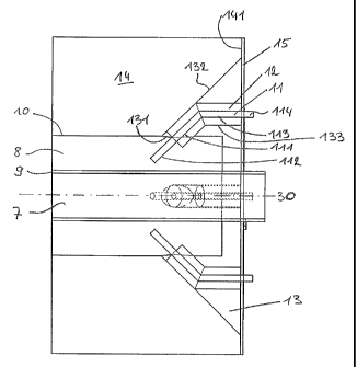
Figures 3 and 4 are schematic rear view and a schematic longitudinal section
view, respectively, of the transducer 2. In this embodiment four probes 11
penetrate
into the outer coaxial waveguide section 8 and provide electrical coupling to
the TE01
and TE10 modes. The probes 11 preferably are bent. Each probe 11 has a first
portion
111 which is inclined with respect to the longitudinal axis 30 of the
waveguides, the
inclination being towards the end face 141 of the housing 14. A tip 112 of
each probe
11 protrudes into the waveguide 8.
A second portion 113 of each probe 11 is aligned substantially parallel with
the
longitudinal axis 30 of the waveguides. Each probe 11 preferably has some
dielectric
material 12 surrounding the probe 11. This helps to position the probe 11
correctly. A
board 15 is mounted to the end face 141 of the housing 14, perpendicular to
the
longitudinal axis 30 of the waveguides. The board can be secured to the
housing by
any suitable mounting technique. This board can secured to the main body, for
example, by, but not limited to, the use of fixation screws, glue or
sandwiched with an
additional cover. Tips 114, 115, 116 and 117 of the probes 11 connect to the
board 15.
Two combiner circuits 191, 192 are implemented on the board 15 as microstrip
elements. Each combiner circuit 191, 192 connects an opposing pair of probes.
Each
combiner circuit 191, 192 has a respective microstrip interface 201, 202 for
that
polarization. Each combiner circuit implements an approximately differential
combination, i.e. approximately 180 relative phase difference, of the two
signals
derived from the pair of probes. Each combiner circuit preferably also
provides some
degree of termination for the sum signal with the resistors 161 and 162, that
is the
hybrid ideally implements a 180 sum-delta hybrid, as shown in Figure 15.
Hence,
using matrix notation for the transfer functions, the operation with an
idealized hybrid
is given by, but ignoring common phase offsets:
Output201 _ 0.5 - 0.5 PYobe114
Res161 0.5 0.5 PYobe115
Because each pair of connected probes are oppositely oriented in the
waveguide, they
have opposite phase coupling to the parallel oriented TE01 mode, and hence
their
signals, after the 180 shift provided by the combining circuit 191, combine
CA 02640478 2008-07-28
WO 2007/087821 PCT/EP2006/000797
7
approximately in phase at the combiner output 201. Also, because the probes
preferably do not couple to the orthogonal TE10 mode, an amount of cross-polar
isolation can be obtained, even with non-ideal combiner circuits. The probes
114 and
115 ideally have in-phase coupling with the TEM mode of the coaxial waveguide
and
hence, because of the combiner circuit phase relation, the TEM mode is to some
extent
coupled to the 0 sum signal port terminated with resistor 161, whereas the
contribution to the output 201 is effectively cancelled due to the 180 shift.
Hence, the
TEM mode is to some degree, coupled to the resistor 161, and therefore some
degree
of termination is provided. This helps to reduce parasitic resonances in the
TEM mode
of the coaxial waveguide. Again using matrix notation, the idealized operation
can be
summarized as follows, but ignoring common phase offsets:
Probe114 _ 0.5 a 0.5 TE01
PYobell S - 0.5 a 0.5 TEM
where lal < 1.
Together with the idealized hybrid transfer matrix shown before, we obtain:
Port201 _ 1 0 TE01
Res161 0 a TEM
Similarly for Port202, we obtain:
Port202 1 0 TEIO
Res162 0 a TEM
Figure 5 is a schematic rear view of the embodiment of the transducer 2, witli
the planar lower frequency combiner circuit removed for clarity. The main
housing has
a set of appropriately shaped cavities 13. The channels 13 allow the probes 11
and their
dielectric surrounding 12 to be inserted into position during the
manufacturing
assembly process. This is possible, even when the main housing 14 is made of a
single
part preferably suitable for mass manufacturing, for example, suitable
manufacturing
CA 02640478 2008-07-28
WO 2007/087821 PCT/EP2006/000797
8
or fabrication techniques such as, but not limited to, metal molding or
plastic molding
with metallic coating. As shown in Figure 5, each channel 13 is located where
a probe
needs to be positioned in the waveguide and extends radially from an entry
position to
the waveguide (131 shown in Figure 4) to the end face 141. During assembly the
channel 13 serves to guide the probe into position. The diameter of the
channel, at the
end nearest waveguide 8, is equal to, or just greater than that of the probe
11 and
dielectric shroud 12 such that the probe 11 is supported by a frictional fit
in the
required position, or is held in place due to the shape of the cavity and the
presence of
the board 15 and/or the preferably solder connection to the microstrip on
board 15.
Referring again to Figure 4, each channel 13 is generally funnel-shaped. The
radially outermost wall 132 of the channel 13 is aligned with portion 111 of
the probe
and extends between the wall of waveguide 8 and the end face 141 of the
housing 14.
The radially innermost wall 133 of the channel 13 has a dog-leg shape, with a
first part
extending from the wall 10 of the waveguide 8 at an angle inclined with
respect to axis
30. This first part is spaced from, and parallel to, the radially-outermost
side 132. A
second part of the wall 133 extends parallel with axis 30 and meets the end
face 141.
During assembly, a non-straight or bent-shaped probe 11 is inserted into a
respective
channel 13 at an angle which is inclined with respect to the longitudinal axis
30. The
probe slides along wall 132 of the channel 13. The probe is stopped when the
dielectric
shrouds 12 touches wall 133, thereby defining the amount the tip 112 extends
into the
waveguide 8. At this point, the probe part 113 between the bent and probe end
114 is
substantially perpendicular to the end face 141 and parallel with the
longitudinal axis
of the waveguides. The board 15 is then mounted to end face 141 of the housing
and probe tips 114 are soldered to the board 15.
25 The dimensions of the channel 13, probes 11 and their dielectric shrouds 12
can
be optimized, for example with, but not limited to, electromagnetic 3D
simulation
software, to provide impedance transformation.
Figures 6-9 show two further embodiments of the invention in which
improvements are made to aid in the positioning of probes within the
waveguide.
30 Firstly, Figure 6 and Figure 7 are a schematic front view and a schematic
longitudinal
section view, respectively, of an embodiment of a transducer which includes an
additional element 18 positioned in the outer coaxial waveguide section 8.
Structure 18
is preferably dielectric material and helps to improve alignment tolerances of
the
CA 02640478 2008-07-28
WO 2007/087821 PCT/EP2006/000797
9
probes 11. The element 18 surrounds the inner waveguide tube 9 and allows a
mechanical positioning of the probes 11, thus reducing the tolerances on the
position of
the probes relative to the waveguide 8, and improving mass manufacturing
repeatability. The assembly process is the same as described above. However,
the
probe 11 can now be more reliably positioned within waveguide 8 as probe 11
can be
inserted into a respective channel 13 until probe tip 112 reaches the radially-
outermost
surface of element 18.
Figure 8 and Figure 9 are a schematic front view and a schematic longitudinal
section view, respectively, of an embodiment of a transducer including probes
11 with
extended dielectric shrouding 12 to improve alignment tolerances. The
dielectric
material 12 around the probe 11 is extended past the end of the probe tip 112
so that it
mechanically touches the inner waveguide tube 9. This allows the probe tip 112
to be
positioned at the required depth inside waveguide section 8. This reduces the
tolerances on the position of the probes 11 relative to the waveguide 8 and
improves
mass manufacturing repeatability. In Figure 9 the dielectric 121 has a face
122 suitably
shaped such that it presses across its, preferably, but not necessarily, full
face against
wall 9. It is not essential to provide this inclined face on the dielectric
material; for
example the dielectric could be cut in other ways or shapes but the
penetration depth of
the probe tip 112 is an electrical design parameter and should preferably not
lead to a
free end in case of a perpendicular dielectric end. The design as shown and
described
will provide close tolerances.
Figure 16 is a schematic rear view of an embodiment of the transducer with
hybrid circuit extended for circular polarization; the ideaiized electrical
schematic is
shown in Figure 17. A preferably 90 hybrid 193 is cascaded to the 180
hybrids.
Using matrix notation, the idealized operation ca.n be summarized as follows:
In the waveguide, we have for the linear and circular modes:
TE01 _ 0.5 j 0.5 ). ( LeftCircular
TE10 j 0.5 0.5 RiglztCiYcular
For the idealized 90 hybrid we obtain:
CA 02640478 2008-07-28
WO 2007/087821 PCT/EP2006/000797
Pof=t203 _ 0.5 - j 0.5 Por t201
Port204 j 0.5 0.5 PoYt202
Together with the relations described above for the linear polarization
embodiment, we
obtain:
5
Port203 0.5 -0.5 - 0.5 j 0.5j Probe114
PoYt204 - 0.5 j 0.5j 0.5 -0.5 Probe115
Res161 0.5 0.5 0 0 Pr~obell6 (Equation 1)
Res162 0 0 0.5 0.5 Probe117
and therefore:
PoYt203 1 0 0
LeftCif=culaf-
Pof-t204 0 1 0
10 = RiglitCircular
Res161 0 0 a 0.5 TEM
Res162 0 0 a 0.5
Alternatively, the overall same functionality can be implemented in a hybrid,
or set of
hybrids, with the 4 probes connected to 4 inputs, and with, one or two
outputs, one
output for each circular polarization (i.e. left-hand circular or/and right-
hand circular)
and providing similar relationships as expressed above in equation 1, or part
thereof.
Also, by appropriate design of the hybrid, one or more resistors may be
incorporated as
to provide some degree of termination of the coaxial waveguide TEM mode.
Figure 18 is a schematic rear view of an embodiment of the transducer with an
alternative hybrid circuit with a single output 205 for circular polarization
and
incorporating a termination resistor 163. The idealized electrical schematic
is shown in
Figure 19. The idealized operation is described by the following, but ignoring
common
phase offsets:
Probe114
1Port205 0.5 -0.5 j0.5 - j0.5 Pf=obe115
Res163 a=0.5 a=0.5 a=0.5 a=0.5 Probe116
PYobe117
CA 02640478 2008-07-28
WO 2007/087821 PCT/EP2006/000797
11
and therefore:
Port205 1 0 0 11 LeftCircular
Res163 0 0 aRiglatCircular
TEM
Instead of using four probes under preferably 90 angles and accordingly
designed hybrid or hybrids, the same functionality can be obtained using three
probes
under preferably 120 angles and an accordingly designed hybrid. This can be
done for
one or two linear polarization couplings, or for one or two circular
polarization
couplings. Also, by appropriate design of the llybrid, one or more resistor
may be
incorporated as to provide some degree of termination of the coaxial waveguide
TEM
mode. Figure 20 and Figure 21 are a schematic front view looking into the
coaxial
waveguide interface 4 and a schematic rear view, respectively, of an
embodiinent of
the transducer using 3 probes. Figure 22 is a schematic rear view of this
embodiment,
with the planar lower frequency combiner circuits removed for illustrative
purpose,
thus showing an embodiment of a mechanical inner construction. Figure 23 is a
simplified electrical schematic of this embodimeiit. If only one polarization,
either
linear or circular, is required, two probes may suffice, while still allowing
for some
termination of the TEM mode.
In any of the previous embodiments, it is also possible to incorporate
amplifiers
between the probes and the hybrids, or have them included within the hybrids.
This
provides an improvement in overall performance.
Figures 10-12 show an embodiment of the transducer where the inner, higher
frequency, waveguide 8 continues within the arrangement of second waveguide
probes
11. Figure 12 sllows the waveguide end removed for clarity. It is useful to
extend the
high frequency waveguide as shown, because the probes can be iinplemented then
on
board 15 and the impedance can be optimized as explained below. In this
einbodiment
two probes 23 are mounted within the inner waveguide 8, offset at 90 from one
another.
Probes 23 are mounted on the same planar board 15 as the lower frequency
combiner circuits previously described. The waveguide 8 is continued through,
and
beyond, the board 15. This is achieved by a ring of holes 25 positioned on the
board
15. The holes are metallised in the direction of the longitudinal axis 30 and
are
connected to one another on the surface of the board 15 by a metallised track.
This
CA 02640478 2008-07-28
WO 2007/087821 PCT/EP2006/000797
12
provides some degree of electrical continuity of the waveguide walls 9. The
ring of
holes 25 aligns with the wall 9 of the inner waveguide 8. A closed end cap 22
fits on
the other side of the ring of holes 25. The side wall of the cap 22 has a pair
of cut-outs
24 to allow the interface lines 21 to enter the waveguide region enclosed by
the cap 22.
The cut-outs 24 are spaced from the feeds 21. The probe 23 is formed by
metallised
tracks on board 15. The later provide a dielectric in the waveguide and also
provide
mechanical support for the probes. The probe dimensions and their distance to
the
closed waveguide end 22 preferably are optimized for matching to the
microstrip
interfaces 21. Even though the probes 23 are in the same plane as the lower
frequency
range combiner circuits 19, no cross-over bridges are required to access the
microstrip
interfaces 21 from other circuits placed on the same plane, thus allowing for
a
straightforward construction suitable for mass manufacturing. Though the probe
orientation for the lower and the upper frequency ranges are shown parallel,
and
therefore the linear polarizations at the lower and higher frequency band are
coplanar,
other embodiments may have angled orientation between the frequency ranges.
That is
the planes defined by each probe axis and the waveguide axis are not same for
the
lower and the higher frequency range. Also, other probe configurations for
transition to
circular waveguide can be integrated.
If, instead of linear polarization, one or both circular polarization are
required,
preferably 90 , preferably microstrip, hybrids can be incorporated between the
probes
and the preferably microstrip interfaces.
In the embodiment described above the inner waveguide 8 is extended by a
combination of a ring of metallised holes 25 and an end cap 22. The board 15
lies
across the inner waveguide 8. In an alternative einbodiment, a hole is
provided in
board 15 which allows the waveguide tube 9 to pass through the board 15. An
end cap
fits across the open end of tube 9. Cut-outs are provided in the side wall of
tube 9 to
allow probes, e.g. soldered to interfaces 21, to enter.
Figure 13 and Figure 14 are a schematic front view and a schematic
longitudinal section view, respectively, of the embodiment of a transducer
using the
same principles but extended for three band operation. A third waveguide 26 is
provided for a third frequency range, e.g. C-band, and probes 27 penetrate
into this
waveguide. All principles as used in the lower frequency band waveguide of the
two-
band transducer embodiment described before, can be applied to this third,
lowest,
CA 02640478 2008-07-28
WO 2007/087821 PCT/EP2006/000797
13
frequency range. Though the probe orientation for the second, lower and the
third
lowest frequency ranges are shown parallel in this embodiment, other
embodiments
may have angled orientation between these frequency ranges, thus resulting in
non-
coplanar polarizations for these frequency ranges. Figure 23 is a schematic
front view
of an embodiment of such a tri-band transducer with non-coplanar polarizations
of the
lowest and lower frequency ranges.
The invention is not limited to the embodiments described herein, which may
be modified or varied without departing from the scope of the invention.