Note: Descriptions are shown in the official language in which they were submitted.
CA 02641490 2008-08-05
WO 2007/095386 PCT/US2007/004213
PHOTOVOLTAIC DEVICE WITH NANOSTRUCTURED LAYERS
RELATED APPLICATIONS
[0001] This patent application claims the benefit of, and priority to, United
States
Provisional Patent Application Serial No. 60/772,548, filed on February 13,
2006, titled
"Solar Cells Integrated With IR and UV Absorbing Nanoparticle Layers," and
United States
Provisional Patent Application Serial No. 60/796,820, filed on May 2, 2006,
titled
"Nanocomposite Solar Cell," the disclosures of both of which are hereby
incorporated by
reference in their entirety.
FIELD OF THE INVENTION
0 [0002] In general, the present invention relates to the field of
photovoltaics or solar
cells. More particularly, the present invention relates to photovoltaic
devices having
nanostructured layers.
BACKGROUND OF THE INVENTION
[0003] Increasing oil prices have heightened the importance of developing cost
5 effective renewable energy. Significant efforts are underway around the
world to develop
cost effective solar cells to harvest solar energy. Current solar energy
technologies can be
broadly categorized as crystalline silicon and thin film technologies. More
than 90% of the
solar cells are made from silicon - single crystal silicon, polycrystalline
silicon or amorphous
silicon.
!0 [0004] Historically, crystalline silicon (c-Si) has been used as the light-
absorbing
semiconductor in most solar cells, even though it is a relatively poor
absorber of light and
requires a considerable thickness (several hundred microns) of material.
Nevertheless, it has
proved convenient because it yields stable solar cells with good efficiencies
(12-20%, half to
two-thirds of the theoretical maximum) and uses process technology developed
from the
!5 knowledge base of the microelectronics industry.
[0005] Two types of crystalline silicon are used in the industry. The first is
monocrystalline, produced by slicing wafers (approximately 150mm diameter and
350
microns thick) from a high-purity single crystal boule. The second is
multicrystalline silicon,
made by sawing a cast block of silicon first into bars and then wafers. The
main trend in
SO crystalline silicon cell manufacture is toward multicrystalline technology.
[0006] For both mono- and multicrystalline Si, a semiconductor p-n junction is
1
CA 02641490 2008-08-05
WO 2007/095386 PCT/US2007/004213
formed by diffusing phosphorus (an n-type dopant) into the top surface of the
boron doped
(p-type) Si wafer. Screen-printed contacts are applied to the front and rear
of the cell, with the
front contact pattern specially designed to allow maximum light exposure of
the Si material
with minimum electrical (resistive) losses in the cell.
[0007] Silicon solar cells are very expensive. Manufacturing is. mature and
not
amenable for significant cost reduction. Silicon is not an ideal material for
use in solar cells
as it primarily absorbs in the visible region of the solar spectrum as
illustrated in FIG. 1.
Significant amount of solar radiation comprises of IR photons as shown in FIG.
2. These IR
photons are not harvested by silicon solar cells thereby limiting their
conversion efficiency.
0 [0008] Second generation solar cell technology is based on thin films. Two
main thin
film technologies are Amorphous Silicon as shown in FIG. 3 and Copper Indium
Gallium
Diselenide (CIGS).
[0009] Amorphous silicon (a-Si) was viewed as the "only" thin film PV material
in
the 1980s. But by the end of that decade, and in the early 1990s, it was
dismissed by many
5 observers for its low efficiencies and instability. However, amorphous
silicon technology has
made good progress toward developing a very sophisticated solution to these
problems:
multijunction configurations. Now, commercial, multijunction a-Si modules
could be in the
7%-9% efficiency range. United Solar and Kaneka have built 25 MW facilities
and several
companies have announced plans to build manufacturing plants in Japan and
Germany.
;0 [0010] The key obstacles to a-Si technology are low efficiencies (about 10%
stable),
light-induced efficiency degradation (which requires more complicated cell
designs such as
multiple junctions), and process costs (fabrication methods are vacuum-based
and fairly
slow). All of these issues are important to the potential of manufacturing
cost-effective a-Si
modules.
;5 [0011] Amorphous silicon solar cells also have poor IR absorption and do
not harvest
energy from IR photons of the solar spectrum. Microcrystalline silicon extends
absorption
into longer wavelengths but also has poor absorption in the IR region. A
variety of reflector
designs have been employed to increase IR harvesting in amorphous silicon
solar cells.
These reflectors add significant cost but provide limited benefit, as they are
unable to extend
0 the IR absorption of amorphous silicon beyond 1,000 nm. Significant
efficiency
improvement can be achieved if IR absorbing layers can be developed which can
be cost
effectively integrated with amorphous and microcrystalline silicon solar
cells.
[0012] . Thin film solar cells made from Copper Indium Gallium Diselenide
(CIGS)
absorbers show promise in achieving high conversion efficiencies of 10-12%.
The record
2
CA 02641490 2008-08-05
WO 2007/095386 PCT/US2007/004213
high efficiency of CIGS solar cells (19.2% NREL) is by far the highest
compared with those
achieved by other thin film technologies such as Cadmium Telluride (CdTe) or
amorphous
Silicon (a-Si).
[0013] These record breaking small area devices have been fabricated using
vacuum
evaporation techniques which are capital intensive and quite costly. It is
very challenging to
fabricate CIGS films of uniform composition on large area substrates. This
limitation also
affects the process yield, which are generally quite low. Because of these
limitations,
implementation of production techniques has not been successful for large-
scale, low-cost
commercial production of thin film solar cells and modules and is non-
competitive with
~ today's crystalline silicon solar modules.
[0014] To overcome the limitations of the physical vapor deposition techniques
that
use expensive vacuum equipment, several companies have been developing high
throughput
vacuum processes (ex: DayStar, Global Solar) and non-vacuum processes (ex:
ISET,
Nanosolar) for the fabrication of CIGS solar cells. Using ink technology, very
high active
5 materials utilization can be achieved with relatively low capital equipment
costs. The
combined effect is a low-cost manufacturing process for thin film solar
devices. CIGS can be
made on flexible substrates making it possible to reduce the weight of solar
cells. Cost of
CIGS solar cells is expected to be lower than crystalline silicon making them
competitive
even at lower efficiencies. Two main problems with CIGS solar cells are: (1)
there is no
~ clear pathway to higher efficiency and (2) high processing temperatures make
it difficult to
use high speed roll to roll process and hence they will not be able to achieve
significantly
lower cost structure achievable by amorphous silicon solar cells.
[0015] CIGS solar cells also have poor IR absorption and do not absorb or
harvest
energy from IR photons of the solar spectrum. Efficiency improvement can be
achieved if IR
5 absorbing layers can be developed which can be cost effectively integrated
with CIGS solar
cells.
[0016] There are significant problems with the currently available
technologies. For
example, crystalline silicon solar cells which have >90% market share today
are very
expensive. Solar energy with c-silicon solar cells costs about 25 cents per
kwh as compared
~ to < 10 cents per kwh for fossil fuels. In addition, the capital cost of
installing solar panels is
extremely high limiting its adoption rate. Crystalline solar cell technology
is mature and
unlikely to improve performance or cost competitiveness in near future.
Amorphous silicon
thin film technology is amenable to high volume manufacturing that could lead
to low cost
solar cells. However, amorphous and microcrystal silicon solar cells absorb
only in the
5 visible region and do not harvest any photons in the IR region.
3
CA 02641490 2008-08-05
WO 2007/095386 PCT/US2007/004213
[0017] A number of examples exist in the prior art in combining such IR
absorbing
thin film layers with Silicon layers to increase solar energy conversion
efficiency. IR
absorbing thin film layers used in the literature were deposited through
expensive vacuum
deposition process. Examples in the literature include multijunction cells and
tandem cells.
Examples in the literature include (1) four terminal devices made from two
separate cells and
(2) two terminal devices made by incorporating tunnel junctions. All these
examples known
in the literature are very expensive to produce limiting their commercial
applications.
[0018] The National Renewable Energy Lab (NREL) has initiated a high
efficiency
tandem solar cell program in 2001 with the primary aim of achieving high
efficiencies. A
0 number of semiconductor materials such as SiGe, PbSe, PbS and III-V
materials absorb in the
IR region and can be used to harvest IR photons. Researchers at NREL have
demonstrated
that broadband multijunction solar cells can be prepared by stacking cells
with absorption in
different wavelength ranges. Tandem solar cells use multiple materials with
different
bandgaps in series in a single cell. Significant progress has been made in
building tandem
5 solar cells however many limitations remain. It is unlikely that these
tandem cells will ever
achieve cost competitiveness for commercial applications. These multijunction
tandem cells
are extremely complicated to design (due to current balancing requirements)
and tend to be
quite expensive. Hence these tandem cells are limited for use in defense,
space and terrestrial
applications where cost is not a critical driving factor. However, it is
unlikely that such
0 designs can ever be economical enough to be used for commercial solar cell
applications.
[0019] Next generation solar cell designs required to truly achieve high
efficiencies
with light weight and low cost. Two potential candidates are (1) polymer solar
cells and (2)
nanoparticle solar cells. Polymer solar cells have the potential to be low
cost due to roll to
roll processing at moderate temperatures (< 150C). However, polymers suffer
from two main
5 drawbacks: (1) poor efficiencies due slow charge transport and (2) poor
stability- especially
to UV. Hence it is unlikely that polymer solar cells will be able to achieve
the required
performance to become the next generation solar cell.
[0020] Several research groups have been conducting experimental studies on
quantum dot based solar cells. Best efficiencies reported to date have been
<5%. Main
0 reasons for low efficiencies of these nanoparticle solar cells has been
charge recombination
due to (1) surface charges on the nano particles and (2) poor charge transport
in the polymer
host. Novel synthetic methods need to be developed to prepare quantum dots
without surface
charge effects. To reduce the impact of polymer host on the charge transport
quantum rods
with a large aspect ratio have been suggested. Researchers from University of
California
5 Berkeley have shown that better efficiency can be achieved by using quantum
rods with
> 10:1 aspect ratio.
4
CA 02641490 2008-08-05
WO 2007/095386 PCT/US2007/004213
[0021] IR absorbing nanoparticles have been reported by University of Toronto
and
University of Buffalo. Ted Sargent's team at University of Toronto has made
the infrared
photovoltaics based on solution-processing by suspending lead sulfide
semiconducting
nanocrystals, measuring 4 nanometers (mu) in diameter, in a semiconducting
plastic (Nature
Materials 2005, 4, 138-142). The 4-nm spheres of PbS are smaller than the
radius of an
excited electron's orbit. The effect of this so-called quantum confinement is
that the light
wavelengths at which the quantum dots begin to absorb energy are directly
related to the
crystals' size. This means that by changing the size of the nanocrystals,
plastic solar cell can
be tuned to any wavelengths desired, from the IR to the visible spectrum. By
controlling the
0 size of the nanocrystals solar cells can be tuned to absorb IR light at
wavelengths of 980,
1200, and 1355 nm and turn it into electric current. IR photovoltaics have
greater potential
because half of the energy in sunlight occurs in the IR, at wavelengths
ranging from 700 nm
to 2 microns. Sargent's first IR system has an abysmal-sounding power-
conversion efficiency
of 0.001%.
5 [0022] Efficient IR absorbing Quantum Dot Photovoltaics composed of indium
phosphide (InP) nanocrystals were developed by Paras Prasad's team at
University of Buffalo
(UB). InP quantum dots demonstrated luminescence efficiencies comparable to
other
quantum dots, but they also emit light in longer wavelengths in the red region
of the
spectrum. This is a key advantage because red-light emission means these
quantum dots will
0 be capable of harvesting photons in the IR region. Quantum dots, comprised
of cadmium
selenide, emit mostly in the lower visible wavelength range. Silicon solar
cells act primarily
in the green region, thus capturing only a fraction of the available light
energy. By contrast,
lead selenide quantum dots can absorb in the infrared, allowing for the
development of
photovoltaic cells that can efficiently convert many times more light to
usable energy than
5 can current silicon solar cells. UB group demonstrated 3% quantum efficiency
for the InP
quantum dots. Their work was described in the paper, "Efficient
photoconductive devices at
infrared wavelengths using quantum dot-polymer nanocomposites," published
online Aug.
11, 2005 in Applied Physics Letters.
[0023] Accordingly, many challenges remain and there is significant need for
further
0 developments.
SUMMARY OF THE INVENTION
[0024] Embodiments of the present invention generally relate to the field of
photovoltaics or solar cells. More particularly, the present invention
provides photovoltaic
devices having IR and/or UV absorbing nanostructured layers.
6 [0025] In one aspect, embodiments of the present invention provide a
photovoltaic
5
CA 02641490 2008-08-05
WO 2007/095386 PCT/US2007/004213
device, comprising: a first photoactive layer comprised of a semiconductor
material
exhibiting absorption of radiation substantially in a visible region of the
solar spectrum, and a
second photoactive layer comprised of nanostructured material exhibiting
absorption of
radiation substantially in an IR region of the solar spectrum. A recombination
layer is
disposed between the first and second layers, and configured to promote charge
transport
between the first and second layers.
[0026] In another aspect, the present invention provides a photovoltaic
device,
comprising: a first photoactive layer; a top photoactive layer disposed above
the first layer,
said top photoactive layer comprised of a material exhibiting a bandgap
greater than the band
0 gap of the first layer; and a bottom photoactive layer disposed below the
first layer, said
bottom photoactive layer comprised of a material exhibiting a bandgap lower
than the band
gap of the first layer. In some embodiments, the top photoactive layer
exhibits a bandgap of
2 ev and greater, and the bottom photoactive layer exhibits a bandgap of 1.2
ev and lower.
[0027] In yet another aspect, embodiments of the present invention provide a
5 photovoltaic device comprising: a first photoactive layer comprised of a
semiconductor
material exhibiting absorption of radiation substantially in a visible region
of the solar
spectrum and a top photoactive layer comprised of one or more nanoparticles
exhibiting
absorption of radiation substantially in an UV region of the solar spectrum. A
recoinbination
layer is disposed between the first and top layers, and configured to promote
charge transport
0 between the first and top layers.
[0028] In a further aspect, embodiments of the present invention provides a
photovoltaic device, comprising: a first photoactive layer comprised of
semiconductor
material exhibiting absorption of radiation substantially in a visible region
of the solar
spectrum, and a top photoactive layer comprised of nanostructured material
exhibiting
5 absorption of radiation substantially in an UV region of the solar spectrum
formed above the
first layer. A recombination layer is disposed between the first and top
layers, and configured
to promote charge transport between the first and top layers. A bottom
photoactive layer
comprised of nanostructured material exhibiting absorption of radiation
substantially in an IR
region of the solar spectrum is formed below the first photoactive layer. A
second
~ recombination layer is disposed between the first and bottom layers, and
configured to
promote charge transport between the first and bottom layers.
[0029] The nanostructured material is any suitable material that comprises
nano-sized
materials or particles. These nano-sized materials or particles may be
dispersed in another
material, such as a precursor or carrier compound. For example, in some
embodiments the
5 nanostructured material is a nanocomposite material which comprises hole
conducting or
6
CA 02641490 2008-08-05
WO 2007/095386 PCT/US2007/004213
electron conducting polymers and complimentary nanoparticles dispersed
therein. The
nanocomposite material may be comprised of one or more nanoparticles dispersed
in a
polymer. In other embodiments, the nanostructured material is comprised of any
one or more
of: semiconducting dots, rbds or mulitpods. Multipods may comprise bi, and tri
rod
structures, or other 2 and 3 dimensional structures. Examples of suitable
nanoparticles
materials include, but are not limited to, any one or more of: PbSe, PbS,
CdHgTe, Si or
SiGe. Of particular advantage, the size and/or composition of the
nanoparticles may be
selected to provide a range of radiation absorption, thus increasing the
absorption efficiency
of the device.
~ [0030] In other embodiments, the 'nanostructured material is comprised of a
mixture
of photosensitive nanoparticles and conductive nanoparticles. One or both of
the
photosensitive and conductive nanoparticles may be functionalized. Examples of
conductive
nanoparticles include, but are not limited to, any one or more of: single wall
carbon
nanotubes (SWCNT), Ti02 nanotubes, or ZnO nanowires. Examples of
photosensitive
5 nanoparticles include, but are not limited to, any one or more of: CdSe,
ZnSe, PbSe, InP, Si,
Ge, SiGe, or Group III-V materials.
[0031] In some embodiments, the recombination layer may be comprised of a
doped
layer comprised of a material that conducts charge opposite that of the
nanostructured
material. Thus in some embodiments, the recombination layer will include a
doped layer
J with a charge opposite that of a conducting polymer in the nanostructured
material.
Alternatively, the recombination layer is a doped layer comprised of a
material that conducts
charge opposite that of the nanoparticles in the nanostructured material. The
recombination
layer may further comprise a metal layer and/or an insulator layer coupled to
a doped layer.
[0032] The first photoactive layer may be comprised of any one of: amorphous
5 silicon, single-crystalline silicon, poly-crystalline silicon,
microcrystalline silicon,
nanocrystalline silicon, CdTe, cooper indium gallium diselinide (CIGS), or
Group III-V
semiconductor material. In another embodiment the first photoactive layer is
comprised of an
organic material which is hole conducting or electron conducting. For example,
the first
photoactive layer may be comprised of a P-I-N semiconductor or a P-N
semiconductor. In
) alternative embodiment, first photoactive layer is comprised on any one or
more of: P3HT,
P3OT, MEH-PPV, PCBM, CuPe, PCTBI or C60.
[0033] In one exemplary embodiment the second layer comprised of
nanostructured
material comprises one or more inorganic nanoparticles dispersed in a hole
conducting
polymer, and the recombination layer is comprised of an N+ doped layer; and a
metal layer
5 coupled to said N+ doped layer.
7
CA 02641490 2008-08-05
WO 2007/095386 PCT/US2007/004213
BRIEF DESCRIPTION OF THE FIGURES
[0034] The foregoing and other aspects of the present invention will be
apparent upon
consideration of the following detailed description, taken in conjunction with
the
accompanying drawings, in which like reference characters refer to like parts
throughout, and
in which:
[0035] Figure 1 shows the known absorption spectrum of Amorphous silicon;
[0036] Figure 2 illustrates the known absorption spectrum of Microcrystalline
silicon;
[0037] Figure 3 shows a conventional amorphous silicon solar cell design;
[0038] Figure 4 is a schematic representation of Core-Shell quantum dots
(Examples:
0 PbSe, PbS and InP);
[0039] Figure 5 illustrates Quantum dots (QD) of different size absorb and
emit at
different colors according to embodiments of the present invention;
[0040] Figure 6 illustrates nanoparticles capped with solvents such as tr-n-
octyl
phosphine oxide (TOPO);
5 [0041] Figure 7 shows functionalized Nanoparticles prepared according to
embodiments of the present invention;
[0042] Figure 8 is a schematic drawing showing one embodiment of a
photovoltaic
device of the present invention with IR absorbing or harvesting nanoparticle
layers integrated
with amorphous or microcrystalline silicon layers;
0 [0043] Figure 9 is a schematic diagram illustrating one embodiment of the
recombination layer of the present invention;
[0044] Figure 10 illustrates a schematic drawing showing another embodiment of
a
photovoltaic device of the present invention with IR harvesting nanoparticle
layers integrated
with polycrystalline or single crystal silicon layers;
5 [0045] Figure 11 shows a photovoltaic device having IR harvesting
nanoparticle
layers integrated with CdTe layers according to embodiments of the present
invention;
[0046] Figure 12 depicts a photovoltaic device with IR harvesting nanoparticle
layers
integrated with CIGS layers according to embodiments of the present invention;
[0047] Figure 13 shows a schematic drawing showing one embodiment of a
8
CA 02641490 2008-08-05
WO 2007/095386 PCT/US2007/004213
photovoltaic device of the present invention with UV absorbing or harvesting
nanoparticle
layers integrated with amorphous or microcrystalline silicon layers;
[0048] Figure 14 is a schematic drawing showing one embodiment of a
photovoltaic
device of the present invention with UV harvesting nanoparticle layers
integrated with
polycrystalline silicon or single crystal silicon layers;
[0049] Figure 15 depicts a schematic drawing showing one embodiment of a
photovoltaic device of the present invention with UV harvesting nanoparticle
layers
integrated with CdTe layers;
J0050] Figure 16 illustrates a schematic drawing showing one embodiment of a
0 photovoltaic device of the present invention with UV harvesting nanoparticle
layers
integrated with CIGS layers;
[00511 Figure 17 shows a photovoltaic device with UV & IR absorbing or
harvesting
nanoparticle layers integrated with amorphous or microcrystalline silicon
layers according to
embodiments of the present invention;
5 [0052] Figure 18 illustrates a photovoltaic device with UV & IR harvesting
nanoparticle layers are integrated with polycrystalline or single crystal
silicon layers
according to embodiments of the present invention;
[0053] Figure 19 shows UV & IR harvesting nanoparticle layers integrated with
CdTe,
layers according to embodiments of the present invention;
0 [0054] Figure 20 shows UV & IR harvesting nanoparticle layers are integrated
with
CIGS layers according to embodiments of the present invention;
[0055] Figure 21 illustrates another embodiment of a photovoltaic device of
the
present invention having UV harvesting nanoparticle layers integrated with III-
V
semiconductor layers;
5 [0056] Figure 22 illustrates a four junction crystalline silicon solar cell
integrated
with IR harvesting nanoparticles according to embodiments of the present
invention;
[0057] Figure 23 shows a four junction crystalline silicon solar cell
integrated with
IJV harvesting nanoparticles according to embodiments of the present
invention;
[0058] Figure 24 shows a four junction thin film solar cell integrated with IR
0 harvesting nanoparticles according to embodiments of the present invention;
9
CA 02641490 2008-08-05
WO 2007/095386 PCT/US2007/004213
[0059] Figure 25 depicts a four junction thin film solar cell integrated with
UV
harvesting nanoparticles according to embodiments of the present invention;
[0060] Figure 26 shows a schematic drawing of a nanocomposite photovoltaic
device with light harvesting layer of photosensitive nanoparticles dispersed
in a polymer
precursor according to embodiments of the present invention;
[0061] Figure 27 shows a schematic drawing of a nanocomposite photovoltaic
device with light harvesting layer of photosensitive nanoparticles dispersed
in a mixture of
polymer and polymer precursor according to embodiments of the present
invention;
[0062] Figure 28 depicts a schematic drawing of a nanocomposite photovoltaic
0 device with light harvesting layer of photosensitive nanoparticle sensitized
carbon nanotubes
(SWCNT) dispersed in a polymer precursor according to embodiments of the
present
invention;
[0063] Figure 29 illustrates a nanocomposite photovoltaic device with light
harvesting layer of photosensitive nanoparticle sensitized carbon nanotubes
(SWCNT)
5 dispersed in a mixture of polymer and polymer precursor according to
embodiments of the
present invention;
[0064] Figure 30 shows a nanocomposite photovoltaic device having light
harvesting
layer of photosensitive nanoparticles and conducting nanostructures such as
SWCNT
dispersed in a mixture of polymer and polymer precursor according to
embodiments of the
0 present invention;
[0065] Figure 31 shows a nanocomposite photovoltaic device with light
harvesting
layer of photosensitive nanoparticles and conducting nanostructures such as
SWCNT
dispersed in a mixture of polymer and polymer precursor according to
embodiments of the
present invention; and
5 [0066] Figure 32 is a process flow diagram showing methods for preparing
photovoltaic devices with a light harvesting layer containing a polymerizable
precursor
according to embodiments of the present invention.
DETAILED DESCRIPTION OF THE INVENTION
[0067] Embodiments of the present invention generally relate to the field of
D photovoltaic or solar cells. More particularly, the present invention
provides photovoltaic
devices having IR and/or UV absorbing nanostructured layers. The terms
photovoltaic
device and solar cell(s) may be used interchangeably throughout the
description.
CA 02641490 2008-08-05
WO 2007/095386 PCT/US2007/004213
[0068] Present invention further relates to increasing solar cell efficiency
cost
effectively by integrating IR photon absorbing or harvesting and/or UV photon
absorbing or
harvesting nanostructure materials. In some embodiments the nanostructured
materials are
integrated with one or more of: crystalline silicon (single crystal or
polycrystalline) solar
cells and thin film (amorphous silicon, microcrystalline silicon, CdTe, CIGS
and III-V
materials) solar cells whose absorption is primarily in the visible region. In
some
embodiments, the nanostructured materials are comprised of one or more
nanoparticles
integrated with a first layer of material which exhibits absorption of
radiation substantially in
the visible spectrum. In some embodiments the nanoparticle layer is comprised
of quantum
0 dots, rods or multipods of various sizes. In one example nanoparticles are
sized in the range
of approximately 2 nm to 10 nm, and more typically in the range of
approximately 2 nm to 6
nm, as shown in FIG. 5. Small nanoparticles absorb at the blue end of the
spectrum while the
large size nanoparticles absorb in the red end of the spectrum.
[0069] Nanoparticle layers are preferably comprised of various luminescent
materials.
5 Examples of suitable materials include, but are not limited to, any one or
more of CdSe,
PbSe, ZnSe, CdS, PbS, Si, Ge, SiGe, InP, or Ill-V semiconductors. PbS, PbSe
and SiGe are
examples of IR absorbing nanoparticles. ZnSe is an example of UV absorbing
nanoparticle.
IR absorbing and UV absorbing nanoparticles of various chemistry and particle
sizes can be
prepared by following methods known in the art.
D [0070] In an alternative embodiment, the nanostructured layer(s) are
comprised of a
polymer composite obtained by dispersing nanoparticles in a conducting polymer
matrix. In
some embodiments, the nanoparticles have a core-shell configuration as
illustrated in FIG. 4.
In this case, the core 10 of the core-shell can comprise semiconductor
materials, such as III-
V, II-IV semiconductors, and the like. The shell 20 may be comprised of
another
5 semiconductor material or a solvent, for example TOPO, as shown in FIG. 6.
In some
embodiments, nanoparticles are functionalized, such as with an organic group
to facilitate
their dispersion in conducting polymer matrix. FIG. 7 shows an exemplary
embodiment
where nanoparticles (also referred to herein as quantum dots "QD") are
comprised Group IV,
II-IV, III-V, II-VI, IV-VI materials. Alteinatively, the nanoparticles 30 are
comprised of any
) one or more of CdSe, PbSe, ZnSe, CdS, PbS, Si, SiGe or Ge. In some example
the
nanoparticles are functionalized with fiuictional groups 40 such as carboxylic
(-COOH),
amine (-NH2), Phosfonate (-P04), Sulfonate (-HSO3), Aminoethanethiol, and the
like.
[0071] Nanoparticle layers can be deposited by known solution processing
methods
such as spin coating, dip coating, ink-jet printing, and the like.
Nanoparticles can also be
5 deposited by vacuum deposition techniques, where applicable. Thickness,
particle sizes,
luminescent materials type, type of polymer materials (if used) and the
nanoparticle loading
11
CA 02641490 2008-08-05
WO 2007/095386 PCT/US2007/004213
level in the polymer composite (if polymer composite is used) can be adjusted
to maximize
absorption in the IR region for IR absorbing nanoparticles and in the UV
region for the UV
absorbing nanoparticles.
[0072] In other embodiments, the nanostructured material is comprised of a
mixture
of photosensitive nanoparticles and conductive nanoparticles. One or both of
the
photosensitive and conductive nanoparticles may be functionalized. Examples of
conductive
nanoparticles include, but are not limited to, any one or more of: single wall
carbon
nanotubes (SWCNT), Ti02 nanotubes, or ZnO nanowires. Examples of
photosensitive
nanoparticles include, but are not limited to, any one or more of: CdSe, ZnSe,
PbSe, InP, Si,
0 Ge, SiGe, or Group III-V materials.
[0073] In another aspect, the present invention relates to the development of
photovoltaic device architectures that promote efficient nanoparticle based
photovoltaic
devices. In some embodiments, photosensitive nanoparticles (quantum dots,
rods, bipods,
tripods, multipods, wires, and the like) are dispersed in a precursor of a
high mobility
5 conducting polymer to form a radiation or light harvesting thin film layer
which is
sandwiched between two conducting electrodes, at least one of these electrodes
is transparent.
The precursors are preferably of low molecular weight so they can conformally
coat the
nanoparticles when a thin film of precursor/nanoparticle is formed after
removal of the
solvent. Nanoparticles can also be functionalized in such a way to facilitate
conformal
0 coating of nanoparticles with precursor. The precursor is then polymerized
either by thermal
means or by using UV radiation to obtain a thin film in which photosensitive
nanoparticles
are fully encapsulated in the high mobility conducting polymer and facilitate
rapid charge
transfer of holes and electrons generated when the nanoparticles are exposed
to light.
[0074] Photosensitive nanoparticles can be made from other photosensitive
materials
5 which generate electron hole pairs when exposed to light. Nanoparticles can
be made from
Cadmium Selenide (CdSe), Zinc Selenide (ZnSe), Lead Selenide (PbSe), Indium
Phosphide
(InP), Lead Sulfide (PbS), Silicon (Si), Germanium (Ge), Silicon-Germanium
(SiGe), Ill-V
materials, and the like.
[0075] Nanoparticles can be functionalized with organic or inorganic
functional
D groups. In such embodiments functional groups attached to the surface of
nanoparticles
include but are not limited to and one or more of: -COOH (carboxylic), -P04
(phosfonate), -
SO3H (sulfonate) and -NH2 (amine).
[0076] Examples of high mobility conducting polymers include but are not
limited to:
Pentacene, P3HT, PEDOT, and the like. Precursors for these polymers may
contain one or
5 more thermally polymerizable functional groups. Epoxy is an example a
suitable thermally
12
CA 02641490 2008-08-05
WO 2007/095386 PCT/US2007/004213
polymerizable functional group. Alternately the precursors may contain one or
more UV
polymerizable functional group. Acrylic fiunctional group is an example of a
suitable UV
polymerizable functional group.
[0077] In some embodiments, a second conducting polymer material is combined
with the precursor of high mobility polymer and photosensitive nanoparticles
to aid in the
initial film formation before the precursor is polymerized. PVK is an example
of a suitable
secondary polymeric material. It is preferred that the precursor and secondary
polymer be
mixed at a maximum ratio of precursor to secondary polymer, as long as the
phase separation
does not occur after polymerization. In one embodiment pentacene is precursor
that is
0 expected to plasticize the PVK film allowing uniform dispersion of
photosensitive
nanoparticles in the film and also allowing conformal coating of nanoparticles
with the
precursor.
[0078] In some embodiments, the layer of nanostructured material is comprised
of a
mixture of photosensitive and conductive nanoparticles. Conductive
nanoparticles such as
5 carbon nanotubes, Ti02 nanotubes, ZnO nanowires can be mixed with the
precursor and
photosensitive nanoparticles (optionally with the second conducting polymer)
to further
enhance charge separation of electrons and holes generated by the
nanoparticles upon their
exposure to light.
[0079] In other embodiments, photosensitive nanoparticles are discreet
particles, or
0 alternatively they are attached to conducting nanostructures such as carbon
nanotubes
(SWCNT), Ti02 nanotubes or ZnO nanowires.
[0080] Photosensitive nanoparticles can be chemically attached to the
conducting
nanostructures based on carbon nanotubes via molecular self assembly so as to
form mono
layers of these nano particles on the carbon nanotubes. Conducting carbon
nanotubes are
5 prepared by methods known in the art. In some embodiments, carbon nanotubes
are
preferably comprised of single wall carbon nanotubes (SWCNT). The carbon
nanotubes can
be functionalized to facilitate their dispersion in suitable solvents.
Functionalized
nanoparticles are reacted with a suitable functional groups (ex: carboxylic or
others) on
carbon nanotubes to deposit a monolayer of dense continuous nanoparticles by
molecular self
0 assembly process. By adjusting the functional group on the nanoparticles and
the carbon
nanotubes, the distance between the surface of the nanostructure and
nanoparticle can be
adjusted to minimize the effect of surface states in facilitating charge
recombination. This
distance is maintained such that electrons tunnel through this gap from the
nanoparticles to
the highly conducting nanostructures. In some embodiments this distance is a
few angstroms,
5 preferably less than 5 angstroms. This facile electron transport will
eliminate charge
13
CA 02641490 2008-08-05
WO 2007/095386 PCT/US2007/004213
recombination and result in efficient charge separation which will lead to
efficient solar
energy conversion. In one embodiment, photosensitive nanoparticles are
attached to the
carbon nanotubes by reacting them in a suitable solvent. Conducting carbon
nanotubes may
be grown directly on a substrate (ex: metal foil, glass coated with conducting
oxide such as
ITO) by following methods known in the art. Photosensitive nanoparticles can
be attached
to the carbon nanotubes grown on the substrate.
[0081] In another aspect of the present invention photovoltaic device
architectures
are taught wherein photosensitive nanoparticles of different sizes are
dispersed in a precursor
of high mobility polymer to form a single layer sandwiched in between two
electrodes with at
0 least one of these electrodes is transparent. A second polymer and/or
conducting
nanostructures are optionally mixed in the layer containing the nanoparticles
and the
precursor.
[0082] Further, embodiments of the present invention provide photovoltaic
device
architectures with multi-layer structure in which each layer comprises
photosensitive
5 nanoparticles of one or more sizes are dispersed in a precursor of high
mobility polymer to
form a single layer sandwiched in between two electrodes with at least one of
these
electrodes is transparent. A second polymer and/or conducting nanostructures
are optionally
mixed in each of these layers containing the nanoparticles and the precursor.
[0083] The present invention further provides photovoltaic devices in which
carbon
!0 nanotubes attached with photosensitive nanoparticles of different materials
of different sizes
dispersed in the precursor of high mobility polymer (optionally combined with
a second
polymer) form a single layer sandwiched in between two electrodes. At least
one of these
electrodes is transparent. Embodiments of the present invention comprise
photovoltaic
devices in which carbon nanotubes attached with photosensitive nanoparticles
of single size
!5 are stacked together to form multiple layers sandwiched in between two
electrodes, with at
least one of these electrodes is transparent. Additionally, the present
invention provides
photovoltaic devices where carbon nanotubes attached with photosensitive
nanoparticles of
single material of single size are stacked together to form multiple layers
sandwiched in
between two electrodes, with at least one of these electrodes is transparent.
In another
embodiment, photovoltaic devices are provided comprising carbon nanotubes
attached with
photosensitive nanoparticles of single material of multiple sizes are stacked
together to form
multiple layers sandwiched in between two electrodes, where at least one of
these electrodes
is transparent.
[0084] In another aspect, embodiments of the present invention provide
photovoltaic
35 devices comprising hole transporting interface layers disposed in between
electrode and
14
CA 02641490 2008-08-05
WO 2007/095386 PCT/US2007/004213
nanocomposite layers. Embodiments include photovoltaic devices in which
electron
transporting interface layers are used in between electrode and nanocomposite
layer.
[0085] Examples of illustrative embodiments are now described with reference
to the
Figures. Referring to FIG. 8, one embodiment of a photovoltaic device 800 of
the present
invention is shown. In this embodiment photovoltaic device is built on a
glass, metallic or
plastic substrate 810 by depositing an insulating layer 820 and metal layer
830 by methods
well known in the art. Layer 840 of nanostructured material with an absorption
in the IR
region 800-2,000nm (with a bandgap of 1.2 ev and less) is deposited on the
metal layer 830
followed by a recombination layer which comprises a transparent conducting
layer (for
0 example ITO) or a tunnel-junction layer 850. These layers are followed by
formation of a
first photoactive layer 855 disposed above the nanostructured layer 840. In
this embodiment,
first photoactive layer 855 is comprised of standard amorphous silicon layers
that include of
n-type amorphous silicon 860, i-type amorphous silicon 870 and p-type
amorphous silicon
880. Alternatively, first photoactive layer 855 may be comprised of
microcrystalline silicon
5 layers which also include n-type microcrystalline silicon, i-type
microcrystalline silicon and
p-type microcrystalline silicon. First photoactive layer 855 may be formed by
methods well
known in the art. A transparent conducting layer (TCO) 890 such as ITO is then
deposited on
top of the silicon layer. Photovoltaic device is oriented such that sunlight
8100 falls on the
TCO 890. The thickness of the amorphous or microcrystalline silicon layers 855
can be
0 adjusted to maximize absorption in the visible region of the solar spectrum.
Photovoltaic
device described in this embodiment will harvest visible and IR photons from
the solar
spectrum resulting in higher conversion efficiency compared to the
photovoltaic device
design without integrating IR absorbing nanoparticles.
[0086] Of particular advantage, a recombination layer or tunnel junction layer
850 is
5 disposed between the first photoactive layer and the nanostructured layer.
In some
embodiments, the recombination layer may be comprised of a doped layer
comprised of a
material that conducts charge opposite that of the nanostructured material.
Thus in some
embodiments, the recombination layer will include a doped layer with a charge
opposite that
of a conducting polynier in the nanostructured material. Alternatively, the
recombination
0 layer is a doped layer comprised of a material that conducts charge opposite
that of the
nanoparticles in the nanostructured material. The recombination layer may
further comprise
a metal layer and/or an insulator layer coupled to doped layer.
[0087] FIG. 9 illustrates recombination layer 850 in more detail. The
recombination
layer 850 is also sometimes referred to in the Examples below as tunnel
junction layer.
5 Nanostructured layer 840 is comprised of a hole conducting material, which
may be hole
conducting nanoparticles, or nanoparticles dispersed in a hold conducting
material, such as a
CA 02641490 2008-08-05
WO 2007/095386 PCT/US2007/004213
hole conducting polymer. Recombination layer 850 comprises a layer of
inetaVand or
insulator and a layer of p doped material. In general, the recombination layer
is a doped layer
comprised of a material that conducts charge opposite that of the
nanostructured layer. Thus,
the recombination layer is a doped layer 850B comprised of a material that
conducts charge
opposite that of the nanoparticle, or of the conducting polymer depending on
the material of
the nanostructured layer 840. In some embodiments, the recombination layer
further
comprises a metal layer 850A coupled to doped layer 850B. Altematively the
recombination
layer further comprises an insulating layer (not shown) coupled to doped layer
850B.
[0088] To provide a proper top and bottom cell connection for the photovoltaic
device
0 of the present invention an interface or recombination layer 850 is provided
as generally
illustrated in FIG. 9. In one embodiment, the recombination layer may have an
additional
layer of heavily doped amorphous silicon with the type of doping opposite to
the
nanostructured layers of the device and / or thin metal or insulating layer
between the first
photoactive layer and the nanostructured layer, which may be thought of as top
and bottom
5 solar cells. The recombination layer is configures to promote charge
transport between the
layers. Specifically, the recombination layer is configures such that the
energy band
configuration is favorable for a significant enhancement of the recombination
rate between
the holes from the bottom nanostructured layers 840 (also referred to as the
bottom cell) and
electrons from the first photoactive layers 855 (also referred to as the top
cell). At the same
0 time the SS participation in the e-h recombination process is suppressed by
physical
separation between the top and bottom cells.
[0089] Referring again to FIG. 9, the top cell has an extra heavily doped P+
layer
850B deposited on the heavily doped N+ contact layer of the first photoactive
layer 855,
which in this embodiment is the N+ region of a P-I-N semiconductor. The above
P+ and N+
5 layers form a tunnel junction at their interface with extra P+ layer 850B
actually becoming a
part of the hole conducting component of the bottom nanostructured layer 840.
The first and
nanostructured layers 855 and 840,respectively are physically separated by a
thin tunnel film
850A of metal. In some embodiment, the metal film 850A is comprised of gold
(Au) and
preferably has a thickness in a range of approximately 5-15A. Other metal
films can be used
0 in other embodiments provided they are thin enough to ensure direct hole
tunneling from the
nanostructured layers while not causing any significant optical or electrical
losses at the
interface. Alternatively, an insulting material may be used instead of a metal
material. It
should be noted that the present invention can be effectively used in
photovoltaic device
embodiments of opposite types of conductivity in which case extra N+ layer
will replace the
5 P+ layer of this embodiment and the nanostructured layer is designed in such
that the upper
contact layer is electron conducting and not hole conducting.
16
CA 02641490 2008-08-05
WO 2007/095386 PCT/US2007/004213
[0090] A corresponding band diagram is also shown in Fig. 9. It can be seen
that
with the recombination interface of the present invention, favorable energy
conditions are
created for the holes coming from the nanostructured or bottom cell to be
transferred to the
extra P+ layer of the top cell through the thin metal film, followed by direct
tunneling and
recombination with the electrons in the N+ layer of the top cell thus
providing an efficient
low resistive and minimal loss connection in series for the top and bottom
cells. Hence the
present invention represents an efficient solution for the problem of proper
connection of top
and bottom cell.
Further Examples of Photovoltaic Devices with IR Absorbiniz Layers
0 [0091] Another embodiment of a photovoltaic device of the present invention
is
illustrated in FIG. 10. Generally, in this embodiment, the layer of
nanostructured material is
comprised of IR harvesting nanoparticle layers integrated with polycrystalline
or single
crystalline silicon layer. The polycrystalline or signal crystal silicon layer
forms the first
photovoltaic layer of a material that absorbs radiation substantially in the
visible range of the
5 solar spectrum. In this embodiment the polycrystalline silicon photovoltaic
device is built by
methods well known in the art by starting with an n-type polycrystalline wafer
1040 and
doping it with a p-type dopant (alternately p-type single crystal wafer can be
doped with n-
t)pe dopant) on one side of the wafer followed by a transparent conductor or a
conducting
grid 1050. A transparent conducting layer (ex: ITO) or a tunnel-junction layer
1030 is
,0 deposited on the polycrystalline silicon wafer on the opposite side of the
first TCO layer
1050. Nanoparticle layer 1020 with an absorption in the IR region 800-2,000nm
(with a
bandgap of 1.2 ev and less) is deposited on the TCO or tunnel junction layer
1030 followed
by a metal layer 1010. The thickness of polycrystalline silicon layers and the
dopant
concentrations can be adjusted to maximize absorption in the visible region of
the solar
,5 spectrum. Photovoltaic device described in this embodiment will harvest
visible and IR
photons from the solar spectrum resulting in higher conversion efficiency
compared to the
photovoltaic device design without integrating IR absorbing nanostructures.
[0092] In yet another embodiment, photovoltaic device is provided where the
first
photoactive layer is comprised of CdTe material as illustrated in FIG. 11.
Here the layer of
0 nanostructured material comprises IR harvesting nanoparticle layers. In this
embodiment
photovoltaic device is built on a glass, metallic or plastic substrate 1110 by
depositing an
insulating layer 1120 and metal layer 1130 by methods well known in the art.
Nanoparticle
layer 1140 with an absorption in the IR region 800-2,000nm (with a bandgap 1.2
ev and less)
is deposited on the metal layer 1130 followed by a transparent conducting
layer (ex: ITO) or
5 a tunnel-junction layer 1150, which comprises the recombination layer. These
layers are
17
CA 02641490 2008-08-05
WO 2007/095386 PCT/US2007/004213
followed by a CdTe layer 1160 which is formed by methods well known in the
art. A
transparent conducting layer TCO 1170 such as ITO is then deposited on top of
the silicon
layer. Photovoltaic device is oriented such that sunlight 1180 falls on the
TCO 1170. The
thickness of CdTe layer can be adjusted to maximize absorption in the visible
region of the
solar spectrum. Photovoltaic device described in this embodiment will harvest
visible and IR
photons from the solar spectrum resulting in higher conversion efficiency
compared to the
photovoltaic device design without integrating IR absorbing nanoparticles.
[0093] In a further embodiment as shown in FIG. 12, IR harvesting nanoparticle
layers are integrated with CIGS layers. In this embodiment photovoltaic device
is built on a
0 glass, metallic or plastic substrate 1210 by depositing an insulating layer
1220 and metal
layer 1230 by methods well known in the art. The nanoparticle layer 1240 with
an absorption
in the IR region 800-2,000nm (with a bandgap of 1.2 ev and less) is deposited
on the metal
layer 1230 followed by a transparent conducting layer (ex: ITO) or a tunnel-
junction layer
1250, which comprises the recombination layer.. These layers are followed by
CIGS layers
5 1260 which are formed by methods well known in the art. A transparent
conducting layer
TCO 1270 such as ITO is then deposited on top of the silicon layer.
Photovoltaic device is
oriented such that sunlight 1280 falls on the TCO 1270. Thickness of CdTe
layer can be
adjusted to maximize absorption in the visible region of the solar spectrum.
Photovoltaic
device described in this embodiment will harvest visible and IR photons from
the solar
0 spectrum resulting in higher conversion efficiency compared to the
photovoltaic device
design without integrating IR absorbing nanoparticles.
Examples of Photovoltaic Device with UVAbsorbing Layers
[0094] In another aspect of the present invention, a photovoltaic device is
provided
wherein a first photoactive layer is comprised of a semiconductor material
exhibiting
5 absorption of radiation substantially in a visible region of the solar
spectrum and a top
photoactive layer is comprised of one or more nanoparticles exhibiting
absorption of
radiation substantially in an UV region of the solar spectrum. A recombination
layer is
disposed between the first and top layers, and configured to promote charge
transport
between the first and top layers. Referring to FIG. 13 is shown a top
photoactive layer of UV
0 harvesting nanoparticle layers are integrated with a first photoactive layer
comprised of
amorphous or microcrystalline silicon layers. In this embodiment photovoltaic
device is built
on a glass, metallic or plastic substrate 1310 by depositing an insulating
layer 1320 and metal
layer 1330 by methods well known in the art. These layers are followed by
standard
amorphous or microcrystalline silicon layers which form the first photoactive
layer in this
,5 embodiment and comprise n-type amorphous silicon 1340, i-type amorphous
silicon 1350
18
CA 02641490 2008-08-05
WO 2007/095386 PCT/US2007/004213
and p-type amorphous silicon 1360 by methods well known in the art. A
transparent
conducting layer TCO or tunnel-junction layer 1370 (in this case the
recombination layer) is
then deposited on top of the silicon layer as the recombination layer.
Nanoparticle layer 1380
with an absorption in the UV region (with a bandgap of 2 ev and higher) is
deposited on the
TCO or tunnel-junction layer 1370 followed by a transparent conducting layer
such as ITO
1390. Photovoltaic device is oriented such that sunlight (100) falls on the
TCO (90).
Thickness of amorphous silicon layers can be adjusted to maximize absorption
in the visible
region of the solar spectrum. Photovoltaic device described in this embodiment
will harvest
visible and UV photons from the solar spectrum resulting in higher conversion
efficiency
0 compared to the photovoltaic device design without integrating UV absorbing
nanoparticles.
[0095] In another embodiment as shown in FIG. 14, UV harvesting nanoparticle
layers are integrated with polycrystalline or single crystal silicon layers.
In this embodiment
polycrystalline or single crystal silicon photovoltaic device is built by
methods well known in
the art by starting with an n-type polycrystalline wafer 1420 and doping it
with a p-type
5 dopant (alternately p-type single crystal wafer can be doped with n-type
dopant) on one side
of the wafer followed by a metal layer 1410. A transparent conducting layer
(ex: ITO) or a
tunnel-junction layer 1430 ( also referred to as recombination layer) is
deposited on the
polycrystalline silicon wafer on the opposite side of the metal layer 1410.
Nanoparticle layer
1440 with an absorption in the UV region (with a bandgap of 2 ev and higher)
is deposited on
'0 the TCO or tunnel junction layer 1430 followed by a TCO layer 1450.
Thickness of
polycrystalline silicon layers and the dopant concentrations can be adjusted
to maximize
absorption in the visible region of the solar spectrum. Photovoltaic device
described in this
embodiment will harvest visible and UV photons from the solar spectrum
resulting in higher
conversion efficiency compared to the photovoltaic device design without
integrating UV
!5 absorbing nanostructures.
[0096] In another embodiment as shown in FIG. 15, UV harvesting nanoparticle
layers are integrated with CdTe layers. In this embodiment photovoltaic device
is built on a
glass, metallic or plastic substrate 1510 by depositing an insulating layer
1520 and metal
layer 1530 followed by CdTe layer 1540 by methods well known in the art. A
transparent
30 conducting layer (ex: ITO) or a tunnel-junction layer 1550 ( in this case
the recombination
layer) is deposited on the CdTe layer 1540 followed by nanoparticle layer 1560
with an
absorption in the UV region (with a bandgap of 2 ev and higher) followed by a
transparent
conducting layer TCO 1570 such as ITO is then deposited on top of the
nanoparticle layer.
Photovoltaic device is oriented such that sunlight 1580 falls on the TCO 1570.
Thickness of
35 CdTe layer can be adjusted to maximize absorption in the visible region of
the solar
spectrum. Photovoltaic device described in this embodiment will harvest
visible and UV
photons from the solar spectrum resulting in higher conversion efficiency
compared to the
19
CA 02641490 2008-08-05
WO 2007/095386 PCT/US2007/004213
photovoltaic device design without integrating UV absorbing nanoparticles.
[0097] In yet another embodiment as shown in FIG. 16, UV harvesting
nanoparticle
layers are integrated with CIGS layers. In this embodiment photovoltaic device
is built on a
glass, metallic or plastic substrate 1610 by depositing an insulating layer
1620 and metal
layer 1630 followed by CIGS layers 1640 by methods well known in the art. A
transparent
conducting layer (ex: ITO) or a tunnel junction layer 1650 (also referred to
as recombination
layer) is deposited on the CIGS layer 1640 followed by nanoparticle layer 1660
with an
absorption in the UV region (with a bandgap of 2 ev and higher) followed by a
transparent
conducting layer TCO 1670 such as ITO is then deposited on top of the
nanoparticle layer.
0 Photovoltaic device is oriented such that sunlight 1680 falls on the TCO
1670. Thickness of
CIGS layer can be adjusted to maximize absorption in the visible region of the
solar
spectrum. Photovoltaic device described in this embodiment will harvest
visible and UV
photons from the solar spectrum resulting in higher conversion efficiency
compared to the
photovoltaic device design without integrating UV absorbing nanoparticles.
5 Examples of Photovoltaic Devices with UV and IR AbsorbingLeers
[0098] In a further aspect, embodiments of the present invention provides a
photovoltaic device, comprising: a first photoactive layer comprised of
semiconductor
material exhibiting absorption of radiation substantially in a visible region
of the solar
spectrum, and a top photoactive layer comprised of nanostructured material
exhibiting
0 absorption of radiation substantially in an UV region of the solar spectrum
formed above the
first layer. A recombination layer is disposed between the first and top
layers, and configured
to promote charge transport between the first and top layers. A bottom
photoactive layer
comprised of nanostructured material exhibiting absorption of radiation
substantially in an IR
region of the solar spectrum is formed below the first photoactive layer. A
second
5 recombination layer is disposed between the first and bottom layers, and
configured to
promote charge transport between the first and bottom layers.
[0099] Referring to FIG. 17 is shown a top layer of UV & harvesting
nanoparticle
layers and a bottom layer of IR harvesting nanoparticles layers with a first
photoactive layer
disposed there between. In this embodiment, the first photoactive layer
comprises amorphous
0 or microcrystalline silicon layers. In this embodiment photovoltaic device
is built on a glass,
metallic or plastic substrate 1710 by depositing an insulating layer 1720 and
metal layer 1730
by methods well known in the art. Nanoparticle layer 1740 with an absorption
in the IR
region 800-2,000nm (with a bandgap less than 1.2 ev) is deposited on the metal
layer 1730
followed by a transparent conducting layer (ex: ITO) or a tunnel-junction
layer (or
5 recombination layer) 1750. These layers are followed by depositing of the
first photoactive
CA 02641490 2008-08-05
WO 2007/095386 PCT/US2007/004213
layer, in this case standard amorphous or microcrystalline silicon layers that
comprise n-type
amorphous silicon 1760, i-type amorphous silicon 1770 and p-type amorphous
silicon 1780,
formed by methods well known in the art. A transparent conducting layer TCO
1790 or
tunnel-junction layer is then deposited on top of the silicon layer.
Nanoparticle layer 17100
with an absorption in the UV region (with a bandgap higher than 2 ev) is
deposited on the
TCO or tunnel-junction layer (90) followed by a transparent conducting layer
such as ITO
17110. Photovoltaic device is oriented such that sunlight 17120 falls on the
TCO 1790.
Thickness of amorphous silicon layers can be adjusted to maximize absorption
in the visible
region of the solar spectrum. Photovoltaic device described in this embodiment
will harvest
.0 visible, UV and IR photons from the solar spectrum resulting in higher
conversion efficiency
compared to the photovoltaic device design without integrating UV and IR
absorbing
nanoparticles.
[00100] Another embodiment is depicted in FIG. 18 which shows UV & IR
harvesting
nanoparticle layers are integrated with polycrystalline or single crystal
silicon layers. In this
.5 embodiment polycrystalline or single crystal silicon photovoltaic device is
built by methods
well known in the art by starting with an n-type polycrystalline wafer 1840
and doping it with
a p-type dopant (alternately p-type single crystal wafer can be doped with n-
type dopant) on
one side of the wafer followed by an TCO or tunnel-junction layer 1830. A
transparent
conducting layer (ex: ITO) or a tunnel-junction layer (also referred to as
recombination layer)
!0 1860 is deposited on the polycrystalline silicon wafer on the opposite side
of the first TCO or
tunnel-junction layer 1830. Nanoparticle layer 1860 with an absorption in the
UV region
(with a bandgap higher than 2 ev) is deposited on the TCO or tunnel junction
layer 1830
followed by a TCO layer 1870. Nanoparticle layer 1820 with an absorption in
the IR region
(with a bandgap less than 1.2 ev) is deposited on the TCO or tunnel junction
layer 1830
!5 followed by a metal electrode layer 1810. Thickness of polycrystalline
silicon layers and the
dopant concentrations can be adjusted to maximize absorption in the visible
region of the
solar spectrum. Photovoltaic device described in this embodiment will harvest
visible, UV
and IR photons from the solar spectrum resulting in higher conversion
efficiency compared to
the photovoltaic device design without integrating UV and IR absorbing
nanostructures.
00 [00101] FIG. 19 illustrates another embodiment where 21 UV & IR harvesting
nanoparticle layers are integrated with CdTe layers. In this embodiment
photovoltaic device
is built on a glass, metallic or plastic substrate 1910 by depositing an
insulating layer 1920
and metal layer 1930 followed by nanoparticle layer 1940 with an absorption in
the IR region
(with a bandgap less than 1.2 ev) followed by a transparent conducting layer
TCO layer 1950
3 or tunnel-junction layer. CdTe layer 1960 is then deposited on TCO or tunnel-
junction layer
( or recombination layer) 1950 by methods well known in the art. A transparent
conducting
layer (ex: ITO) or a tunnel junction layer 1970 is deposited on the CdTe layer
1960 followed
21
CA 02641490 2008-08-05
WO 2007/095386 PCT/US2007/004213
by nanoparticle layer 1980 with an absorption in the UV region (with a bandgap
greater than
2 ev) followed by a transparent conducting layer TCO 1990 such as ITO is then
deposited on
top of the nanoparticle layer. Photovoltaic device is oriented such that
sunlight 19100 falls on
the TCO 1990. Thickness of CdTe layer can be adjusted to maximize absorption
in the
visible region of the solar spectrum. Photovoltaic device described in this
embodiment will
harvest visible, UV and IR photons from the solar spectrum resulting in higher
conversion
efficiency compared to the photovoltaic device design without integrating UV
and IR
absorbing nanoparticles.
[00102] FIG. 20 illustrates yet another embodiment where UV & IR harvesting
0 nanoparticle layers are integrated with CIGS layers. In this embodiment
photovoltaic device
is built on a glass, metallic or plastic substrate 2010 by depositing an
insulating layer 2020
and metal layer 2030 followed by nanoparticle layer 2040 with an absorption in
the IR region
(with a bandgap less than 1.2 ev) followed by a transparent conducting layer
TCO layer or
tunnel-junction layer ( or recombination layer) 2050 . CIGS layers 2060 are
then deposited
5 on TCO or tunnel-junction layer 2050 by methods well known in the art. A
transparent
conducting layer (ex: ITO) or a tunnel-junction layer 2070 is deposited on the
CIGS layers
2060 followed by nanoparticle layer 2080 with an absorption in the UV region
(with a
bandgap greater than 2 ev) followed by a transparent conducting layer TCO 2090
such as
ITO is then deposited on top of the nanoparticle layer. Photovoltaic device is
oriented such
:0 that sunlight 20100 falls on the TCO 2090. Thickness of CIGS layers can be
adjusted to
maximize absorption in the visible region of the solar spectrum. Photovoltaic
device
described in this embodiment will harvest visible, UV and IR photons from the
solar
spectrnm resulting in higher conversion efficiency compared to the
photovoltaic device
design without integrating UV and IR absorbing nanoparticles.
!5 [00103] In another aspect of the present invention, compound semiconductor
materials
may be employed as the first photoactive layer which absorbs radiation
substantially in the
visible region of the solar spectrum. FIG. 21 illustrates a photovoltaic
device with UV
harvesting nanoparticle layers (ex: InP quantum dots) integrated with III-V
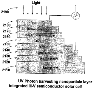
semiconductor
layers (ex: GaAs). In this embodiment photovoltaic device is built on a
substrate 2110 by
SO depositing an insulating layer 2120 and metal layer 2130 by methods well
known in the art.
These layers are followed by III-V semiconductor layers that consist of p-type
semiconductor
2140 and n-type semiconductor 2150 by methods well known in the art. A
transparent
conducting layer TCO 2160 or tunnel-junction layer is then deposited on top of
the Ill-V
layer. Nanoparticle layer 2170 with an absorption in the UV region (with a
bandgap higher
35 than 2 ev) is deposited on the TCO or tunnel-junction layer (also referred
to as recombination
layer) 2160 followed by a transparent conducting layer 2180. Photovoltaic
device is oriented
such that sunlight 2190 falls on the TCO 2180. Photovoltaic device described
in this
22
CA 02641490 2008-08-05
WO 2007/095386 PCT/US2007/004213
embodiment will harvest visible and W photons from the solar spectrum
resulting in higher
conversion efficiency compared to the photovoltaic device design without
integrating W
absorbing nanoparticles.
Examples ofFour Junction Photovoltaic Devices
> [00104] Some embodiments of the present invention provide a four junction
photovoltaic device. FIG. 22 illustrates an IR harvesting nanoparticle
photovoltaic device
and a crystalline (single crystal or polycrystalline) photovoltaic device is
integrated to form a
four junction photovoltaic device. In this embodiment crystalline silicon
photovoltaic device
is built by methods well known in the art by starting with an n-type
crystalline silicon wafer
} 2280 and doping it with a p-type dopant (alternately p-type silicon wafer
can be doped with
n-type dopant) on one side of the wafer followed by a transparent conducting
layer 2270.
Crystalline silicon photovoltaic device is completed by depositing a
transparent conducting
layer (ex: ITO) or a tunnel-junction layer (the first recombination layer)
2290 on the silicon
wafer on the opposite side of the first TCO layer 2270. Photovoltaic device
containing IR
> absorbing nanoparticles is built by starting with a substrate (glass, metal
or plastic) 2210 and
depositing a dielectric layer 2220 followed by metal layer 2230 by using
standard methods
known in the art. A nanoparticle layer 2240 with an absorption in the IR
region (with a
bandgap less than 1 ev) is deposited on the metal layer 2230 followed by a TCO
or tunnel
junction layer (in this case the second recombination layer) 2250. A four
junction tandem cell
} shown in Fig 22 is built by combining the crystalline silicon photovoltaic
device and the IR
absorbing nanoparticle photovoltaic device. An optical adhesive layer 2260 can
be optionally
used to bond the two cells together. Relative performance of the individual
cells can be
adjusted to maximize absorption in the visible and IR region of the solar
spectrum.
Photovoltaic device described in this embodiment will harvest visible and IR
photons from
the solar spectrum resulting in higher conversion efficiency compared to the
photovoltaic
device design without integrating a photovoltaic device containing IR
absorbing
nanostructures.
[00105] FIG. 23 illustrates another embodiment where UV harvesting
nanoparticle
photovoltaic device and crystalline (single crystal or polycrystalline)
silicon photovoltaic
J device are integrated to form a four junction photovoltaic device. In this
embodiment
crystalline silicon photovoltaic device is built by methods well known in the
art by starting
with an n-type crystalline silicon wafer 2320 and doping it with a p-type
dopant (alternately
p-type silicon wafer can be doped with n-type dopant) on one side of the wafer
followed by a
metal layer 2310. Crystalline silicon photovoltaic device is completed by
depositing a
5 transparent conducting layer (ex: ITO) or a tunnel-junction layer (in this
case the first
23
CA 02641490 2008-08-05
WO 2007/095386 PCT/US2007/004213
recombination layer) 2330 on the silicon wafer on the opposite side of the
metal layer 2310.
Photovoltaic device containing UV absorbing nanoparticles is built by starting
with a
transparent substrate (glass, or plastic) 2380 and depositing a transparent
conducting TCO
layer 2370 by using standard methods known in the art. A nanoparticle layer
2360 with an
absorption in the IR region (with a bandgap less than 2 ev) is deposited on
the TCO layer
2370 followed by a TCO or tunnel junction layer (in this case the second
recombination
layer) 2350. A four junction tandem cell shown in Fig 23 is built by combining
the crystalline
silicon photovoltaic device and the IR absorbing nanoparticle photovoltaic
device. An
optical adhesive layer 2340 can be optionally used to bond the two cells
together. Relative
0 performance of the individual cells can be adjusted to maximize absorption
in the visible and
UV region of the solar spectruxn. Photovoltaic device described in this
embodiment will
harvest visible and UV photons from the solar spectrum resulting in higher
conversion
efficiency compared to the photovoltaic device design without integrating a
photovoltaic
device containing UV absorbing nanostructures.
5 [00106] FIG. 24 depicts yet another embodiment where IR harvesting
nanoparticle
photovoltaic device and a thin film (a-Si, u-Si, CdTe, CIGS, III-V)
photovoltaic device is
integrated to form a four junction photovoltaic device. In this embodiment
thin film
photovoltaic device is built by methods well known in the art by starting with
a transparent
substrate 24100 and depositing transparent conducting layer 2490 followed by
active thin
,0 film layer 2480 and a transparent conductor or tunnel junction layer (the
first recombination
layer) 2470. Photovoltaic device containing IR absorbing nanoparticles is
built by starting
with a substrate (glass, metal or plastic) 2410 and depositing a dielectric
layer 2420 followed
by metal layer 2430 by using standard methods known in the art. A nanoparticle
layer 2440
with an absorption in the IR region (with a bandgap less than 1 ev) is
deposited on the metal
!5 layer 2430 followed by a TCO or tunnel junction layer (the second
recombination layer)
2450. A four junction tandem cell shown in Fig 24 is built by combining the
crystalline
silicon photovoltaic device and the IR absorbing nanoparticle photovoltaic
device. An
optical adhesive layer 2460 can be optionally used to bond the two cells
together. Relative
performance of the individual cells can be adjusted to maximize absorption in
the visible and
S0 IR region of the solar spectrum. Photovoltaic device described in this
embodiment will
harvest visible and IR photons from the solar spectrum resulting in higher
conversion
efficiency compared to the photovoltaic device design without integrating a
photovoltaic
device containing IR absorbing nanostructures.
[00107] An additional embodiment of a four junction photovoltaic device
according to
35 embodiments of the present invention is shown in FIG. 25 where UV
harvesting nanoparticle
photovoltaic device and a thin film (a-Si, u-Si, CdTe, CIGS, III-V)
photovoltaic device is
integrated to form a four junction photovoltaic device. In this embodiment
thin film
24
CA 02641490 2008-08-05
WO 2007/095386 PCT/US2007/004213
photovoltaic device is built by methods well known in the art by starting with
a transparent
substrate 25100 and depositing transparent conducting layer 2590 followed by
active thin
film layer 2580 and a transparent conductor or tunnel junction layer (e.g.
first recombination
layer) 2570. Photovoltaic device containing UV absorbing nanoparticles is
built by starting
with a substrate (glass, metal or plastic) 2510 and depositing a dielectric
layer 2520 followed
by metal layer 2530 by using standard methods' known in the art. A
nanoparticle layer 2540
with an absorption in the UV region (with a bandgap less than 1 ev) is
deposited on the metal
layer 2530 followed by a TCO or tunnel junction layer (e.g, second
recombination layer)
2550. A four junction tandem cell shown in Fig 25 is built by combining the
crystalline
0 silicon photovoltaic device and the UV absorbing nanoparticle photovoltaic
device. An
optical adhesive layer 2560 can.be optionally used to bond the two cells
together. Relative
performance of the individual cells can be adjusted to maximize absorption in
the visible and
UV region of the solar spectrum. Photovoltaic device described in this
embodiment will
harvest visible and UV photons from the solar spectrum resulting in higher
conversion
5 efficiency compared to the photovoltaic device design without integrating a
photovoltaic
device containing UV absorbing nanostructures.
Examples ofPh tovoltaic Devices with Functionalized Nanoparticles
[00108] In a further aspect, embodiments of the present invention provides a
photovoltaic device, comprising: a first photoactive layer comprised of
semiconductor
0 material exhibiting absorption of radiation substantially in a visible
region of the solar
spectrum, and on or more photoactive layer comprised of nanostructured
material exhibiting
absorption of radiation substantially in an UV and/or region of the solar
spectrum wherein
one or more of the nanostructured materials comprise functionalized
nanoparticles. FIG. 26
illustrates one embodiment of a nanocomposite photovoltaic device according to
the present
5 invention. This photovoltaic device is formed by coating a thin layer of
nanocomposite 2640
containing photosensitive nanoparticles and precursor of a high mobility
polymer such as
pentacene on a glass substrate 2610 coated with a transparent conductor 2620
such as ITO
followed by the deposition of cathode metal layer 2660. Photosensitive
nanoparticles can be
made from Group IV, II-IV, Il-VI, IV-VI, III-V materials. Examples of
photosensitive
0 nanoparticles include, but are not limited to any one or more of: Si, Ge,
CdSe, PbSe, ZnSe,
CdTe, CdS, or PbS. Nanoparticle sizes can be varied, for example in a range of
approximately 2 nm to 10 nm to obtain a range of bandgaps. These nanoparticles
can be
prepared by methods known in the art. Nanoparticles can be functionalized by
methods
known in the art. Examples of suitable functional groups include, but are not
limited to:
5 carboxylic (-COOH), amine (-NH2), Phosfonate (-P04), Sulfonate (-HSO3),
CA 02641490 2008-08-05
WO 2007/095386 PCT/US2007/004213
Aminoethanethiol, etc. Nanocomposite layer 2640 of photosensitive
nanoparticles dispersed
in precursor of high mobility polymer such as pentacene can be deposited on
ITO coated
glass substrate by spin coating or other well known solution processing
techniques. This
layer can be one monolayer or multiple monolayers. Precursor in the
nanocomposite layer
2640 is polymerized by heating the films to appropriate temperatures to
initiate
polymerization of pentacene precursor. If a UV polymerizable precursor is used
the
polymerization can be achieved by exposing the film to LTV from the ITO side
2620 of FIG.
26. Embodiment of the photovoltaic device may be fabricated according the
method
illustrated in FIG. 32. In this device electron hole pairs are generated when
sunlight is
0 absorbed by the nanoparticles and the resulting electrons are rapidly
transported by the high
mobility polymer such as pentacene to the cathode for collection. This rapid
removal of
electrons from the electron-hole pairs generated by the nanoparticles
eliminates the
probability of electron-hole recombination commonly observed in nanoparticle
based
photovoltaic device devices.
.5 [00109] According to the embodiments shown in FIG. 26, hole
injecting/transporting
interface layer or a buffer layer 2630 may be disposed between ITO 2620 and
nanocomposite
layer 2640. Alternatively, electron injecting/transporting interface layer,
also referred to
recombination layer, 2650 may be disposed between metal layer 2660 and
nanocomposite
layer 2640.
!0 [00110] FIG. 27 depicts another embodiment of nanocomposite photovoltaic
device.
This photovoltaic device is fabricated by coating a nanocomposite layer 2740
comprising
photosensitive nanoparticles, a high mobility polymer such as PVK or P3HT and
a precursor
of a high mobility polymer 2740 such as pentacene on a glass substrate 2710
coated with a
transparent conductor 2720 such as ITO followed by the deposition of cathode
metal layer
!5 2760. Photosensitive nanoparticles comprise Group IV, II-IV, II-VI, IV-VI,
III-V materials.
Examples of photosensitive nanoparticles include, but are not limited to any
one or more of:
Si, Ge, CdSe, PbSe, ZnSe, CdTe, CdS or PbS. Nanoparticle sizes can be varied
(for example
in a range of approximately 2 nm to lOnm) to obtain a range of bandgaps. These
nanoparticles can be prepared by methods known in the art. Nanoparticles can
be
SO functionalized by methods known in the art. Functional groups include, but
are not limited
to: carboxylic (-COOH), amine (-NH2), Phosfonate (-P04), Sulfonate (-HSO3),
Aminoethanethiol, etc. Nanocomposite layer 2740 of photosensitive
nanoparticles dispersed
in high mobility polymer such as PVK or P3HT and a precursor of high mobility
polymer
such as pentacene can be deposited on ITO coated glass substrate by spin
coating or other
35 known solution processing techniques. Nanocomposite layer 2740 can be one
monolayer or
multiple monolayers. In some embodiments, the precursor in the nanocomposite
layer 2740
is polymerized by heating the films to appropriate temperatures to initiate
polymerization of
26
CA 02641490 2008-08-05
WO 2007/095386 PCT/US2007/004213
pentacene precursor. If a UV polymerizable precursor is used the
polymerization can be
achieved by exposing the film to UV from the ITO side 2720. In some
embodiments, the
photovoltaic device is fabricated according to the method shown in FIG. 32.
Photovoltaic
devices built according this embodiment are expected to have high efficiency.
In this device
electron hole pairs are generated when sunlight is absorbed by the
nanoparticles and the
resulting electrons are rapidly transported by the high mobility polymer such
as pentacene to
the cathode for collection. This rapid removal of electrons from the electron-
hole pairs
generated by the nanoparticles eliminates the probability of electron-hole
recombination
commonly observed in nanoparticle based photovoltaic device devices.
0 [00111] Additionally, in some embodiments hole injecting/transporting
interface layer
or a buffer layer 2730 aan be used between ITO 2720 and nanocomposite layer
2740. In an
alternative embodiment, electron injecting/transporting interface layer 2750
can be used
between metal layer 2760 and nanocomposite layer 2740.
Examples ofPdzotovoltaie Devices with Functionalized Nanoparticles and
Conducting
5 Nanoparticles/Nanostructures
[00112] In some embodiments, the nanostructured material is comprised of a
mixture
of photosensitive nanoparticles and conductive nanoparticles. One, or both of,
the
photosensitive and conductive nanoparticles may be functionalized. Examples of
conductive
nanoparticies are comprised of any one or more of: single wall carbon
nanotubes (SWCNT),
0 Ti02 nanotubes, or ZnO nanowires. Examples of photosensitive nanoparticles
are comprised
of any one or more of: CdSe, ZnSe, PbSe, InP, Si, Ge, SiGe, or Group III-V
materials.
[00113] FIG. 28 illustrates an embodiment of nanocomposite photovoltaic
device.
This photovoltaic device can be built by coating a thin layer of nanocomposite
2840
containing photosensitive nanoparticles attached to a conducting nanostructure
dispersed in a
5 precursor of a high mobility polymer such as pentacene on a glass substrate
2810 coated with
a transparent conductor 2820 such as ITO followed by the deposition of cathode
metal layer
2860. Photosensitive nanoparticles can be made from Group IV, II-IV, II-VI, IV-
VI, III-V
materials. Examples of photosensitive nanoparticles include Si, Ge, CdSe,
PbSe, ZnSe,
CdTe, CdS, PbS. Nanoparticle sizes can be varied (for example: 2-lOnm) to
obtain a range
0 of bandgaps. These nanoparticles can be prepared by following the methods
well known in
the art. Nanoparticles can be functionalized by following the methods well
known in the art.
Functional groups can include carboxylic (-COOH), amine (-NH2), Phosfonate (-
P04),
Sulfonate (-HSO3), Aminoethanethiol, etc. Conducting nanostructures can be
made from
carbon nanotubes (SWCNT), Ti02 nanotubes or ZnO nanowires. Conducting
nanostructures
27
CA 02641490 2008-08-05
WO 2007/095386 PCT/US2007/004213
can be functionalized to facilitate the attachment of photosensitive
nanoparticles to the
surface of conducting nanostructures. Nanocomposite layer 2840 of
photosensitive
nanoparticles are attached to conducting nanostructures and dispersed in
precursor of high
mobility polymer such as pentacene. This layer 2840 is deposited on ITO coated
glass
substrate by spin coating or other known solution processing techniques. This
layer can be
one monolayer or multiple monolayers. A precursor in the nanocomposite layer
2840 is
polymerized by heating the films to appropriate temperatures to initiate
polymerization of
precursor. If a LJV polymerizable precursor is used the polymerization can be
achieved by
exposing the film to UV from the ITO side 2820. Methods shown in FIG. 32 may
be carried
0 our to form the photovoltaic device. In this device electron hole pairs are
generated when
sunlight is absorbed by the nanoparticles and the resulting electrons are
rapidly transported
by the conducting nanostructures and high mobility polymer such as pentacene
to the cathode
for collection. This rapid removal of electrons from the electron-hole pairs
generated by the
nanoparticles eliminates the probability of electron-hole recombination
commonly observed
5 in nanoparticle based photovoltaic device devices. Additionally hole
injecting/transporting
interface layer or a buffer layer 2830 can be employed between ITO 2820 and
nanocomposite
layer 2840. In another embodiment, electron injecting/transporting interface
layer 2850 can
be used between metal layer 2860 and nanocomposite layer 2840.
[00114] A further embodiment of nanocomposite photovoltaic device is shown in
FIG.
0 29. This photovoltaic device can be built by coating a nanocomposite layer
2940 containing
photosensitive nanoparticles attached to a conducting nanostructure dispersed
in a high
mobility polymer such as PVK or P3HT and a precursor of a high mobility
polymer such as
pentacene 2940 on a glass substrate 2910 coated with a transparent conductor
2920 such as
ITO followed by the deposition of cathode metal layer 2960. Photosensitive
nanoparticles
5 may comprise Group IV, II-IV, II-VI, IV-VI, Ill-V materials. Examples of
photosensitive
nanoparticles include, but are not limited to any one or more of: Si, Ge,
CdSe, PbSe, ZnSe,
CdTe, CdS, PbS. Nanoparticle sizes can be varied (for example: 2-IOnm) to
obtain a range
of bandgaps. These nanoparticles can be prepared methods well known in the
art.
Nanoparticles can be functionalized by methods well known in the art.
Functional groups
D can include carboxylic (-COOH), amine (-NH2), Phosfonate (-P04), Sulfonate (-
HSO3),
Aminoethanethiol, etc. Conducting nanostructures can be made from carbon
nanotubes
(SWCNT), Ti02 nanotubes or ZnO nanowires.
[00115] . Conducting nanostructures may be functionalized to facilitate the
attachment
of photosensitive nanoparticles to the surface of conducting nanostructures.
In some
5 embodiments, nanocomposite layer 2940 of photosensitive nanoparticles are
attached to
conducting nanostructures and dispersed in high mobility polymer such as PVK
or P3HT. A
precursor of high mobility polymer such as pentacene can be deposited on ITO
coated glass
28
CA 02641490 2008-08-05
WO 2007/095386 PCT/US2007/004213
substrate by spin coating or other well known solution processing techniques.
This layer can
be one monolayer or multiple monolayers. The precursor in the nanocomposite
layer 2940 is
polymerized by heating the films to appropriate temperatures to initiate
polymerization of
pentacene precursor. If a W polymerizable precursor is used the polymerization
can be
achieved by exposing the film to UV from the ITO side 2920. This photovoltaic
device can
be made by using the process flow shown in FIG. 32. Photovoltaic device built
according
this embodiment is expected to have high efficiency. In this device electron
hole pairs are
generated when sunlight is absorbed by the nanoparticles and the resulting
electrons are
rapidly transported by the -conducting nanostructures and the high mobility
polymer
0 pentacene to the cathode for collection. This rapid removal of electrons
from the electron-
hole pairs generated by the nanoparticles eliminates the probability of
electron-hole
recombination commonly observed in nanoparticle based photovoltaic device
devices.
[00116] In another embodiment, hole injecting/transporting interface layer or
a buffer
layer 2930 can be used between ITO 2920 and nanocomposite layer 2940.
Alternatively,
5 electron injecting/transporting interface layer 2950 can be used between
metal layer 2960 and
nanocomposite layer 2940.
[00117] Yet a further embodiment of nanocomposite photovoltaic device is shown
in
FIG. 30. This photovoltaic device can be built by coating a thin layer of
nanocomposite 3040
containing photosensitive nanoparticles and conducting nanostructure dispersed
in a
0 precursor of a high mobility polymer such as pentacene on a glass substrate
3010 coated with
a transparent conductor 3020 such as ITO followed by the deposition of cathode
metal layer
3060. Photosensitive nanoparticles can be made from Group IV, II-IV, II-VI, IV-
VI, III-V
materials. Examples of photosensitive nanoparticles include Si, Ge, CdSe,
PbSe, ZnSe,
CdTe, CdS, PbS. Nanoparticle sizes can be varied (for example: 2-lOnm) to
obtain a range
5 of bandgaps. These nanoparticles can be prepared by following the methods
known in the
art. Nanoparticles can be functionalized by following methods known in the
art. Functional
groups can include carboxylic (-COOH), amine (-NH2), Phosfonate (-P04),
Sulfonate (-
HSO3), Aminoethanethiol, etc. Conducting nanostructures can be made from
carbon
nanotubes (SWCNT), Ti02 nanotubes or ZnO nanowires. The conducting
nanostructure can
0 be functionalized to facilitate their dispersal in the precursor of high
mobility polymer.
Nanocomposite layer 3040 of photosensitive nanoparticles and conducting
nanostructures
dispersed in precursor of high mobility polymer such as pentacene can be
deposited on ITO
coated glass substrate by spin coating or other well known solution processing
techniques.
This layer can be one monolayer or multiple monolayers. Precursor in the
nanocomposite
5 layer 3040 is polymerized by heating the films to appropriate temperatures
to initiate
polymerization of precursor. If a UV polymerizable precursor is used the
polymerization can
be achieved by exposing the film to UV from the ITO side 3020. Photovoltaic
device built
29
CA 02641490 2008-08-05
WO 2007/095386 PCT/US2007/004213
according this embodiment is expected to have high efficiency. In this device
electron hole
pairs are generated when sunlight is absorbed by the nanoparticles and the
resulting electrons
are rapidly transported by the conducting nanostructures and the high mobility
polymer such
as pentacene to the cathode for collection. This rapid removal of electrons
from the electron-
hole pairs generated by the nanoparticles eliminates the probability of
electron-hole
recombination commonly observed in nanoparticle based photovoltaic device
devices. In
some embodiments, hole injecting/transporting interface layer or a buffer
layer 3030 can be
used between ITO 3020 and nanocomposite layer 3040. Alternatively, electron
injecting/transporting interface layer 3050 can be used between metal layer
3060 and
0 nanocomposite layer 3040.
[00118] FIG. 31 depicts yet another embodiment of nanocomposite photovoltaic
device. This photovoltaic device can be built by coating a nanocomposite layer
3140
comprising photosensitive nanoparticles and conducting nanostructures
dispersed in a high
mobility polymer such as PVK or P3HT and a precursor of a high mobility
polymer such as
5 pentacene 3140 on a glass substrate 3110 coated with a transparent conductor
3120 such as
ITO followed by the deposition of cathode metal layer 3160. Photosensitive
nanoparticles
can be made from Group. IV, II-IV, II-VI, IV-VI, III-V materials. Examples of
photosensitive nanoparticles include Si, Ge, CdSe, PbSe, ZnSe, CdTe, CdS, PbS.
Nanoparticle sizes can be varied (for example: 2-lOnm) to obtain a range of
bandgaps. These
0 nanoparticles can be prepared by following the methods known in the art.
Nanoparticles can
be functionalized by following the methods known in the art. Functional groups
can include
carboxylic (-COOH), amine (-NH2), Phosfonate (-P04), Sulfonate (-HSO3),
Aminoethanethiol, etc. Conducting nanostructures can be made from carbon
nanotubes
(SWCNT), Ti02 nanotubes or ZnO nanowires. Conducting nanostructure can be
5 functionalized to facilitate their dispersion in conducting polymer and
precursor of high
mobility polymer. Nanocomposite layer 3140 of photosensitive nanoparticles and
conducting
nanostructures dispersed in high mobility polymer such as PVK or P3HT and a
precursor of
high mobility polymer such as pentacene can be deposited on ITO coated glass
substrate by
spin coating or other well known solution processing techniques. This layer
can be one
0 monolayer or multiple monolayers. Precursor in the nanocomposite layer 3140
is
polymerized by heating the films to appropriate temperatures to initiate
polymerization of
pentacene precursor. If a UV polymerizable precursor is used the
polymerization can be
achieved by exposing the film to UV from the ITO side. Photovoltaic device
shown in FIG.
31 can be made by using the method steps illustrated in FIG. 32. Photovoltaic
device built
5 according this embodiment is expected to have high efficiency. In this
device electron hole
pairs are generated when sunlight is absorbed by the nanoparticles and the
resulting electrons
are rapidly transported by the conducting nanostructures and the high mobility
polymer
CA 02641490 2008-08-05
WO 2007/095386 PCT/US2007/004213
pentacene to the cathode for collection. This rapid removal of electrons from
the electron-
hole pairs generated by the nanoparticles eliminates the probability of
electron-hole
recombination commonly observed in nanoparticle based photovoltaic device
devices.
[00119] In a version of this embodiment shown in FIG. 31, hole
injecting/transporting
interface layer or a buffer layer 3130 can be used between ITO 3120 and
nanocomposite
layer 3140. Alternatively, electron injecting/transporting interface layer
3150 can be used
between metal layer 3160 and nanocomposite layer 3140.
[00120] The above embodiments are some examples of the applying the present
invention. It will be understood to any one skilled in the art that other
transparent conducting
D materials such as Zinc Oxide, Tin Oxide, Indium Tin Oxide, Indium Zinc Oxide
can be used
in the above embodiments. It will be understood to any one skilled in the art
that the
photosensitive nanoparticles can have various shapes - dots, rods, bipods,
multipods, wires
etc. It will be understood to any one skilled in the art that other conducting
nanotube
materials can be used in place of carbon nanotubes, Ti02 nanotubes and ZnO
nanotubes
5 described in the embodiments. It will be understood to any one skilled in
the art that other
heat curable or radiation curable precursors can be used in place of the
pentacene precursors.
It will be understood to any one skilled in the art that other conducting
polymers can be used
in place PVK, P3HT and PEDOT. It will be understood to any one skilled in the
art that a
mixture of conducting and non-conducting polymer can be used in place of
conducting
0 polymers PVK, P3HT and PEDOT described in the embodiments.
[00121] FIG. 32 illustrates one embodiment of a method which may be utilized
to
prepare photovoltaic devices according to some embodiments of the present
invention.
Specifically, a substrate is coated with ITO at step 3210. A buffer layer may
optionally be
deposited atop the ITO coated substrate at step 3220. The device then
undergoes solution
5 coating at step 3240. Optionally, the solution may contain photosensitive
nanoparticles,
polymer precursor and a polymer, step 3230. A buffer layer may optionally be
deposited
after solution coating, step 3250. Next, metal is deposited at step 3260, and
finally the
precursor is polymerized at step 3270. Polymerization may occur by thermal or
UV
exposure.
D [00122] The foregoing descriptions of specific embodiments and best mode of
the
present invention have been presented for purposes of illustration and
description only. They
are not intended to be exhaustive or to limit the invention to the precise
forms disclosed.
Specific features of the invention are shown in some drawings and not in
others, for purposes
of convenience only, and any feature may be combined with other features in
accordance
5 with the invention. Steps of the described processes may be reordered or
combined, and
31
CA 02641490 2008-08-05
WO 2007/095386 PCT/US2007/004213
other steps may be included. The embodiments were chosen and described in
order to best
explain the principles of the invention and its practical application, to
thereby enable others
skilled in the art to best utilize the invention and various embodiments with
various
modifications as are suited to the particular use contemplated. Further
variations of the
invention will be apparent to one skilled in the art in light of this
disclosure and such
variations are intended to fall within the scope of the appended claims and
their equivalents.
The publications referenced above are incorporated herein by reference in
their entireties.
32