Note: Descriptions are shown in the official language in which they were submitted.
CA 02641537 2008-10-22
1
TOUCH SENSOR FOR A DISPLAY SCREEN OF AN ELECTRONIC
DEVICE
[0001]This application relates generally to the field of
touch sensors for electronic devices, and more specifically,
to touch sensors for display screens of handheld, wireless,
and other electronic devices.
[0002]Handheld electronic devices may have a number of
different configurations. Examples of such devices include
personal data assistants ("PDAs"), handheld computers, two-
way pagers, cellular telephones, and the like. Many handheld
electronic devices also feature wireless communication
capability, although many other handheld electronic devices
are stand-alone devices that are functional without
communication with other devices.
[0003]Such handheld electronic devices are generally intended
to be portable, and thus are of a relatively compact
configuration in which keys and other input structures often
perform multiple functions under certain circumstances or
may otherwise have multiple aspects or features assigned
thereto.
[0004]In addition to using keys on a keypad, handheld
electronic devices may also use a touchscreen. A touchscreen
is a display screen overlay which provides the ability to
display and receive information on the same display screen.
The effect of the overlay is to allow a display screen to be
used as an input device, possibly removing the keys on the
keypad as the primary input device for interacting with the
display screen's content. Display screens with integrated
touchscreens can make computers and handheld electronic
devices more useable. A touchscreen or touchscreen system
typically includes a touch sensor, a controller or
processor, and accompanying software. The controller
CA 02641537 2008-10-22
2
communicates user selections to the processor of the
electronic device in which the touchscreen is used.
[0005]One problem with existing LCD touchscreen displays
relates to the arrangement of their touch sensors. In
existing LCD touchscreen displays, in order to provide a
number of input pads in an X/Y matrix arrangement, the touch
sensor typically consists of two stacked indium tin oxide
("ITO") polyethylene terephthalate ("PET") polyester film
layers. The first ITO PET film layer may include a number of
rows of input pads (X inputs), the input pads in each row
being connected in series. The second ITO PET film layer may
include a number of columns of input pads (Y inputs), the
input pads in each column being connected in series.
However, this arrangement has several problems as follows.
[0006]First, the use of two ITO PET film layers increases the
overall material and production costs of the touch sensor.
In addition, the two stacked ITO PET film layers reduce the
light transitivity and optical performance of the LCD
touchscreen display.
[0007]Second, for on-screen keypad applications, it is
difficult to distinguish between two adjacent icons. To
achieve higher resolution, the X/Y matrix has to be expanded
by adding additional rows and/or columns of input pads.
However, the addition of more rows and/or columns means that
additional input channels are required for the controller
(i.e., each row or column requiring a separate input
channel), which in some cases, is not possible. Additional
traces for the additional row and column input channels
translates into a requirement for additional routing space
around the perimeter of the display which in turn results in
a larger display. However, in many applications, larger
displays cannot be accommodated.
CA 02641537 2008-10-22
3
[0008]Third, the use of additional input channels requires
increased scanning times for the input pads and hence
increased response times. In applications involving haptic
feedback or gesture-based input, for example, increased
response times are often not acceptable.
[0009]Fourth, it can be difficult to align icons presented on
the display with the appropriate input pads of the X/Y
matrix. As such, finger shadow effects may lead to the
selection of wrong inputs.
[0010]Fifth, the increased density of controller input
channel traces required for a higher resolution X/Y matrix
effectively limits the size of the display that can be used.
For example, a 1.8" display may be implemented at high
resolution but a 3.5" display may not be practical as the
increased density of the required controller input channel
traces may simply take up too much space.
[0011]A need therefore exists for an improved touch sensor
for a display screen of a handheld, wireless, or other
electronic device. Accordingly, a solution that addresses,
at least in part, the above and other shortcomings is
desired.
GENERAL
[0012]According to one aspect of the application, there may
be provided a touch sensor for mounting over a display
screen of an electronic device, comprising: an elongate
input pad formed in a layer of transparent conductive
material on a transparent substrate, the input pad tapering
from a broad end to a narrow end to provide an input pad
capacitance that varies with location of a touch over the
input pad; and, a contact for coupling the input pad to a
processor.
CA 02641537 2008-10-22
4
[0013]According to another aspect of the application, there
may be provided a touch sensor keypad for mounting over a
display screen of an electronic device, comprising: at least
one elongate input pad formed in a layer of transparent
conductive material on a transparent substrate, the input
pad tapering from a broad end to a narrow end to provide a
respective input pad capacitance for each of a plurality of
locations of a touch over the input pad; and, a contact for
coupling the input pad to a processor; wherein the input pad
forms a column or row of the keypad; and, wherein each of
the plurality of locations of the touch corresponds to a
respective key in the column or row of the keypad; whereby
the input pad provides multi-touch functionality for the
column or row of the keypad.
BRIEF DESCRIPTION OF THE DRAWINGS
[0014]Features and advantages of the embodiments of the
present application will become apparent from the following
detailed description, taken in combination with the appended
drawings, in which:
[0015]FIG. 1 is a front view illustrating a handheld
electronic device in accordance with an embodiment of the
application;
[0016]FIG. 2 is a block diagram illustrating a processing
system for the device of FIG. 1;
[0017]FIG. 3 is a top view illustrating a touch sensor and
transparent cover for the device of FIG. 1;
[0018]FIG. 4 is a screen capture illustrating a keypad
presented on the display screen of FIG. 1;
[0019]FIG. 5 is a screen capture illustrating a multimedia
controller presented on the display screen of FIG. 1;
CA 02641537 2008-10-22
[0020]FIG. 6 is a top view illustrating an alternate touch
sensor for the device of FIG. 1; and,
[0021]FIG. 7 is a top view illustrating a portion of an
alternate touch sensor for the device of FIG. 1.
5[0022]It will be noted that throughout the appended drawings,
like features are identified by like reference numerals.
DESCRIPTION OF PREFERRED EMBODIMENTS
[0023]In the following description, details are set forth to
provide an understanding of the application. In some
instances, certain software, circuits, structures and
techniques have not been described or shown in detail in
order not to obscure the application. Embodiments of the
present application may be implemented in any computer
programming language provided that the operating system of
the data processing system provides the facilities that may
support the requirements of the application. Any limitations
presented would be a result of a particular type of
operating system or computer programming language and would
not be a limitation of the present application.
[0024]According to one embodiment, there is provided a touch
sensor for mounting over a display screen of an electronic
device, comprising: an elongate input pad formed in a layer
of transparent conductive material on a transparent
substrate, the input pad tapering from a broad end to a
narrow end to provide an input pad capacitance that varies
with location of a touch over the input pad; and, a contact
for coupling the input pad to a processor.
[0025]According to another embodiment, there is provided a
touch sensor keypad for mounting over a display screen of an
electronic device, comprising: at least one elongate input
pad formed in a layer of transparent conductive material on
a transparent substrate, the input pad tapering from a broad
CA 02641537 2008-10-22
6
end to a narrow end to provide a respective input pad
capacitance for each of a plurality of locations of a touch
over the input pad; and, a contact for coupling the input
pad to a processor; wherein the input pad forms a column or
row of the keypad; and, wherein each of the plurality of
locations of the touch corresponds to a respective key in
the column or row of the keypad; whereby the input pad
provides multi-touch functionality for the column or row of
the keypad.
[0026]FIG. 1 is a front view illustrating a handheld
electronic device 100 in accordance with an embodiment of
the application. And, FIG. 2 is a block diagram illustrating
a processing system 200 for the device 100 of FIG. 1. The
exemplary handheld electronic device 100 includes a housing
110 in which is disposed a processing system 200 that
includes an input apparatus 210, an output apparatus 220, a
processor (or controller) 230, memory 240, and one or more
hardware and/or software modules 250. The processor 230 may
be, for example and without limitation, a microprocessor and
is responsive to inputs from the input apparatus 210 and
provides output signals to the output apparatus 220. The
processor 230 also interfaces with the memory 240.
[0027]The handheld electronic device 100 may be a two-way
communication device having voice and/or advanced data
communication capabilities, including the capability to
communicate with other computer systems. Depending on the
functionality provided by the device 100, it may be referred
to as a data messaging device, a two-way pager, a cellular
telephone with data messaging capabilities, a wireless
Internet appliance, a data communication device (with or
without telephony capabilities), a wireless fidelity ("Wi-
Fi") device, a wireless local area network ("WLAN") device,
CA 02641537 2008-10-22
7
a wireless device, a handheld device, or a wireless handheld
device.
[0028]According to one embodiment, the input apparatus 210
may include a keypad 120, a thumbwheel 130 or other input
device such as a trackball, various buttons, etc., and a
touchscreen 140. In addition to the keypad 120, the
thumbwheel 130 can serve as another input member since the
thumbwheel 130 is capable of being rotated and depressed
generally toward the housing 110. Rotation of the
thumbwheel 130 provides selection inputs to the processor
230, while depression of the thumbwheel 130 provides another
selection input to the processor 230.
[0029]The output apparatus 220 includes a display screen 150
(e.g., a liquid crystal display ("LCD")) upon which can be
provided an output 180 such as a graphical user interface
("GUI"), a speaker 170, etc. An exemplary GUI 180 is shown
on the display screen 150 in FIG. 1. The display screen 150
has associated circuitry and a controller or processor
(e.g., 230, 240, 250) for receiving information from the
processor of the handheld electronic device 100 for
presentation.
[0030]The processor 230 is coupled to the input apparatus
210, output apparatus 220, and memory 240 for receiving user
commands or queries and for displaying the results of these
commands or queries to the user on the display screen 150.
To provide a user-friendly environment to control the
operation of the device 100, operating system ("0/S")
software modules 250 resident on the device 100 provide a
basic set of operations for supporting various applications
typically operable through the GUI 180 and supporting GUI
software modules 250. For example, the 0/S provides basic
input/output system features to obtain input from the keypad
120, the thumbwheel 130, and the like, and for facilitating
CA 02641537 2008-10-22
8
output to the user through the display screen 150, the
speaker 170, etc. Though not shown, one or more applications
for managing communications or for providing personal
digital assistant like functions may also be included.
According to one embodiment, the device 100 is provided with
hardware and/or software modules 250 for facilitating and
implementing various additional functions.
[0031]A user may interact with the device 100 and its various
software modules 250 using the GUI 180. GUIs are supported
by common operating systems and provide a display format
which enables a user to choose commands, execute application
programs, manage computer files, and perform other functions
by selecting pictorial representations known as icons, or
items from a menu through use of an input or pointing device
such as a thumbwheel 130 and keypad 120. In general, a GUI
is used to convey information to and receive commands from
users and generally includes a variety of GUI objects or
controls, including icons, toolbars, drop-down menus, pop-up
menus, text, dialog boxes, buttons, and the like.
[0032]A user typically interacts with a GUI 180 presented on
a display screen 150 by using an input or pointing device
(e.g., a thumbwheel 130, a keypad 120, etc.) to position a
pointer or cursor over an object (i.e., "pointing" at the
object) and by "clicking" on the object (e.g., by depressing
the thumbwheel 130, by depressing a button on the keypad
120, etc.). This is often referred to as a point-and-click
operation or a selection operation. Typically, the object
may be hi-lighted (e.g., shaded) when it is pointed at.
[0033]Typically, a GUI based system presents application,
system status, and other information to the user in
"windows" appearing on the display screen 150. A window is a
more or less rectangular area within the display screen 150
in which a user may view an application or a document. Such
CA 02641537 2008-10-22
9
a window may be open, closed, displayed full screen, reduced
to an icon, increased or reduced in size, or moved to
different areas of the display screen 150. Multiple windows
may be displayed simultaneously, such as: windows included
within other windows, windows overlapping other windows, or
windows tiled within the display area.
[0034]The display screen 150 of the device 100 has
touchscreen capability provided by the touchscreen 140. The
touchscreen 140 has a touch sensor (300 in FIG. 3)
positioned over top of display screen 150 or integrated into
the display screen 150. The display screen 150 and touch
sensor 300 may be protected by a transparent cover or lens
190 positioned over the touch sensor 300 and display screen
150 or integrated into the display screen 150 or touch
sensor 300.
[0035]Also shown on the display screen 150 as part of output
180 is a button or slidebar icon 160. The button or slidebar
icon 160 may be touched by a user to generate an input
through operation of the touchscreen 140. By touching the
button or slidebar icon 160, for example, an input may be
sent to the processor 230 to initiate an operation (e.g.,
sending a text message, etc.). The touchscreen 140 has
associated circuitry and a controller or processor (e.g.,
230, 240, 250) for determining where the user's touch was
made on the sensor 300 and for sending the coordinates of
the touch to the processor of the handheld electronic device
100 to determine a corresponding operation (e.g., the
sending of the text message, etc.). In this way, the device
100 supports touchscreen functionality.
[0036]The memory 240 can be any of a variety of types of
internal and/or external storage media such as, without
limitation, RAM, ROM, EPROM(s), EEPROM(s), and the like that
provide registers for data storage such as in the fashion of
CA 02641537 2008-10-22
an internal storage area of a computer, and can be volatile
memory or non-volatile memory. As shown in FIG. 2, the
memory 240 is in electronic communication with the processor
230. The memory 240 additionally includes a number of
5 modules 250 for the processing of data. The modules 250 can
be in any of a variety of forms such as, without limitation,
software, firmware, hardware, and the like. The one or more
modules 250 may be executed or operated to perform methods
of the present application as well as other functions that
10 are utilized by the handheld electronic device 100.
Additionally, the memory 240 can also store a variety of
databases such as, without limitation, look-up tables, a
language database, etc.
[0037]Thus, the handheld electronic device 100 includes
computer executable programmed instructions for directing
the device 100 to implement the embodiments of the present
application. The programmed instructions may be embodied in
one or more hardware or software modules 250 resident in the
memory 240 or processing system 200 of the device 100.
Alternatively, the programmed instructions may be embodied
on a computer readable medium (such as a CD disk or floppy
disk) which may be used for transporting the programmed
instructions to the memory 240 of the device 100.
Alternatively, the programmed instructions may be embedded
in a computer-readable signal or signal-bearing medium that
is uploaded to a network by a vendor or supplier of the
programmed instructions, and this signal or signal-bearing
medium may be downloaded through an interface (e.g., 210) to
the device 100 from the network by end users or potential
buyers.
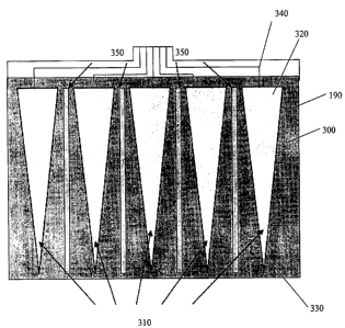
[0038]FIG. 3 is a top view illustrating a touch sensor 300
and transparent cover 190 for the device 100 of FIG. 1. The
CA 02641537 2008-10-22
11
touch sensor 300 includes at least one input pad (or button
or slider) 310 formed in a layer of transparent conductive
material (e.g., ITO, a conductive polymer, etc.) on a
transparent substrate (e.g., a PET film, a glass, etc.). The
input pad 310 tapers from a broad end 320 down to a narrow
end 330. The taper of the input pad 310 provides a
capacitance that varies with location of touch along the
input pad 310. In particular, if a user touches the input
pad 310 at its broad end 320, the impact on the electric
field of the input pad 310 is larger and hence the touch has
a larger effect on the capacitance of the input pad 310. In
addition, if a user touches the input pad 310 at its narrow
end 330, the impact on the electric field of the input pad
310 is smaller and hence the touch has a smaller effect of
on the capacitance of the input pad 310. The capacitance of
the input pad 310 when touched thus provides an indication
of the location of the touch along the input pad 310.
[0039]The input pad 310 includes a contact 340 for coupling
the input pad 310 to a controller or processor 230. The
contact 340 may be located at the broad end 320 of the input
pad 340 as shown in FIG. 3 or at the narrow end 330 of the
input pad 310. Each contact 340 is routed via a trace (e.g.,
a silver trace, etc.) along the edge of the display screen
150 to a tail connector for coupling to the processor 230.
The processor 230 receives a signal indicative of the
capacitance from the input pad 310 and determines the
location of touch from the capacitance. This may be
performed by using a look-up table, for example. The
processor 230 may include functionality similar to, for
example, an AD7147 capacitance sensing integrated circuit
("IC") available from Analog DevicesT". This functionality
may be included in the device's processor 230 or in a
separate device coupled to the processor 230.
CA 02641537 2008-10-22
12
[0040] In FIG. 3, the input pads 310 have an isosceles
triangle shape. However, the input pads 310 may have any
tapered shape (e.g., right triangle shaped, etc.) having a
broad end 320 and a narrow end 330. Also in FIG. 3, the
input pads 310 are shown as being vertically arranged (i.e.,
broad end 320 up, narrow end 330 down). However, the input
pads 310 may also be arranged horizontally (i.e., broad end
320 to the right or left, narrow end 330 to the left or
right) or at any angle (e.g., broad end 320 down, narrow end
330 up). Furthermore, in FIG. 3, five input pads 310 are
shown. However, the number of input pads 310 may vary
depending on the application.
[0041]Also shown in more detail in FIG. 3 is the transparent
cover or lens 190 for the touch sensor 300 and display
screen 150. The lens 190 has ridges (or ribs) 350 formed
thereon for guiding a user's finger between adjacent input
pads 310. Each ridge 350 extends between the broad ends 320
and the narrow ends 330 of adjacent input pads 310. The
ridges 350 may be formed on the transparent cover or lens
190 by injection moulding. The transparent cover or lens 190
may then be laminated to the sensor 300 using an optically
clear adhesive.
[0042]When touched, the capacitance of the input pad 310
provides an indication of the location of the touch along
the input pad 310. As such, the input pad 310 may be used to
initiate multiple operations via multiple icons 160
displayed over the input pad 310 on the display screen 150.
Recall, of course, that the input pad 310 is transparent
when formed on a transparent substrate.
[0043]FIG. 4 is a screen capture illustrating a keypad 400
presented on the display screen 150 of FIG. 1. In FIG. 4,
various icons 160 are presented in rows and columns. Each
column of icons (e.g., TY, GH, BN, SP) is associated with a
CA 02641537 2008-10-22
13
single input pad 310. Because the capacitance of the input
pad 310 varies from top 320 to bottom 330, detection of
which icon 160 a user has selected is possible by
associating the capacitance value of the touch with a
location along the input pad 310 and hence to a position of
a selected icon 160 on the display screen 150.
[0044]FIG. 5 is a screen capture illustrating a multimedia
controller 500 presented on the display screen 150 of FIG.
1. In FIG. 5, various icons 160 are presented in rows and
columns. Each column of icons is associated with a single
input pad 310. Again, because the capacitance of the input
pad 310 varies from top 320 to bottom 330, detection of
which icon 160 a user has selected is possible by
associating the capacitance value of the touch with a
location along the input pad 310 and hence to a position of
a selected icon 160 on the display screen 150. The single
input pad 310 is particularly useful for implementing slide
bar operations through a slide bar icon 160 (e.g., a volume
control slide bar). Because the capacitance varies from top
320 to bottom 330 along the input pad 310 when it is
touched, a smooth slide bar operation may be readily
implemented.
[0045]The rows and columns of icons 160 shown in FIGS. 4 and
5 may be considered to be a X/Y matrix. The X position in
the matrix is determined by which input pad 310 is touched
while the Y position in the matrix is determined by where
along the input pad 310 the touch is made.
[0046]The columns of icons 160 shown in FIGS. 4 and 5 are
aligned with the ridges 350 shown in FIG. 3. The ridges (or
ribs) 350 guide the user's finger to appropriate touch
locations. A ridge 350 is located between each input pad
310. The use of the ridges 350 helps to prevent multiple
touches on an input pad 310. In the operation of a typical
CA 02641537 2008-10-22
14
handheld device 100, a user uses his or her left-hand and
right-hand thumbs to press keys on the keypad 120 of the
device 100. Similarly, a user would use his or her left-hand
and right-hand thumbs to select icons 160 presented on the
display screen 150 of the device 100. In this scenario, the
use of vertical ridges 350 reduces the chance that a user
will select multiple icons 160 in adjacent columns by
activating adjacent input pads 310. Of course, rather than
using his or her left-hand and right-hand thumbs, a user may
also use his or her fingers (e.g., index finger, forefinger,
etc.).
[0047]FIG. 6 is a top view illustrating an alternate touch
sensor 600 for the device 100 of FIG. 1. In FIG. 6, each
input pad 610 has an adjacent correspondingly shaped, but
oppositely oriented, reference pad 620. As such, the
capacitance of the reference pad 620 will vary inversely to
that of the input pad 610 when both pads 610, 620 are
touched at the same location. In FIG. 6, each input pad 610
is right triangle shaped with its broad end towards the top
of the sensor 600. As such, each reference pad 620 is also
right triangle shaped but has its broad end towards the
bottom of the sensor 600. By orientating a pair of input and
reference pads 610, 620 in this way, the likelihood that
both of the input and reference pads 610, 620 in a pair are
touched simultaneously, is increased. The input pads 610 and
reference pads 620 are formed on the same substrate. That
is, only one layer of transparent conductive material is
required. The reference pads 620 allow for a reduction in
noise effects and for improved touch input differentiation
between adjacent input pads 610. With the sensor 600 of FIG.
6, the location of touch along an input pad 610 (i.e., the Y
position in the X/Y matrix referred to above) may be
determined by the ratio of the capacitance of the input pad
CA 02641537 2008-10-22
610 to that of its corresponding reference pad 620 when both
are touched. By using this ratio rather than an absolute
capacitance value, noise effects and the need for
calibration may be reduced making the sensor 600 more
5 tolerant to manufacturing variations.
[0048]FIG. 7 is a top view illustrating an alternate input
and reference pads 710, 720 for the device 100 of FIG. 1. In
FIG. 7, the input pad 710 is isosceles triangle shaped as in
FIG. 4 and the reference pad 720 is in the form of a pair of
10 joined right triangle shaped sections that are shaped to
receive the input pad 710. Of course, an input pad 710 and
its corresponding reference pad 720 may have any
complementary shapes that support the use of a ratio of
capacitance to determine location of touch along the input
15 pad 710.
[0049]The above embodiments may provide one or more
advantages. First, the ridges or ribs 350 formed on the
transparent cover or lens 190 of the display screen 150
provide a useful guide for a user's fingers. Second, the
tapered input pads 310 allow for the implementation of an
X/Y matrix of icons 160 without the use of multiple layers
of transparent conductive material. Third, the use of
tapered input pads 310 reduces the number of input channels
required for a processor 230 implementing an X/Y matrix. For
example, only five input channels are required to implement
the 5X4 matrix of FIG. 4 while a previous two layer solution
would require nine input channels. Fourth, by reducing the
number of transparent conductive material layers, the
optical performance of the display screen 150 is improved
while production costs are reduced. Fifth, a decreased
number of processor input channels allows for faster channel
scanning.
CA 02641537 2008-10-22
16
[0050]The embodiments of the application described above are
intended to be exemplary only. Those skilled in this art
will understand that various modifications of detail may be
made to these embodiments, all of which come within the
scope of the application.