Note: Descriptions are shown in the official language in which they were submitted.
CA 02641878 2008-08-01
WO 2007/091053
PCT/GB2007/000414
- 1 -
OPTICAL MODULATOR
The present invention relates to an optical modulator and a method of
controlling the
same. The invention relates specifically, but not exclusively, to a micro opto-
electro-
mechanical systems (MOEMS) spatial optical modulator for use in an imaging
system.
Spatial optical modulators are of interest for a variety of imaging
applications including
scientific instruments and commercial products.
By way of background to the present invention, MOEMS optical modulators are
known
which utilise optical interference effects to control the intensity and / or
phase of a
beam of light. For example, Lewis et al., SPIE-5614 (1994), pp. 24 ¨ 30
describes an
optical modulator structure based on a MOEMS device with a tuneable gap that
acts as
a resonant optical cavity (silicon-air-silicon Fabry-Perot etalon). The device
described
in Lewis et al. does however differ from most MOEMS optical modulator
structures in
that it may act in transmission as well as reflection.
Goossen et al, IEEE Phot. Tech. Lett. 6 (1994), pp. 1119¨ 1121 describes an
optical
modulator, operated in reflective mode, based on a resonant Fabry-Perot cavity
incorporating a tuneable cavity below a moveable membrane. In the device
referred to
in Goossen et al., the membrane is supported by arms above an air gap and is
moveable by means of electrostatic force resulting from a bias voltage applied
between
an electrode placed around the circumference of the membrane and an underlying
substrate. When the membrane is brought into close proximity with the
underlying
substrate, an anti-reflection condition exists and so the reflected signal is
diminished. In
transmission the contrast between the open and closed states is very low and
the
design would not be suitable as a spatial light modulator for use in the infra-
red spectral
region. Whilst the modulator described in Goossen may be usefully employed in
fibre-
optic communications applications, such a structure is difficult to scale up
into a two-
dimensional arrays having fine pitch geometries (10pm ¨ 50pm) because its fill
factor
would be unacceptably low. In addition, the stresses in the materials used
within the
modulator are such that a more compact support structure could not be realised
without significantly distorting the moveable membrane. Further, the device
referred to
in Goossen et al. is susceptible to distortion due to differential thermal
coefficients of
expansion of the materials used therein (metal over nitride structure). Such
distortion
CA 02641878 2008-08-01
WO 2007/091053
PCT/GB2007/000414
- 2 -
would compromise the optical performance of the device since the resonant
cavity
would be ill-defined.
The electrode being limited to the periphery of the membrane to maximise fill
factor
means only a small proportion of the area is used to drive the device
electrostatically.
Thus high voltages are required to modulate the device. Similarly, the metal
being
above the membrane, increases the inter-electrode gap and reduces the
resulting force
unless a higher drive voltage is applied. The finite size of the upper
electrode required
on the device and associated drive voltages makes this device unsuitable for
scaling to
small pixel sizes (15-50pm) required for large area (two dimensional) arrays
with high
pixel counts.
US patent 5,636,052 describes a reflective display comprising a two-
dimensional
spatial optical modulator having an array of MOEMS optical modulators. Each
modulator within the array comprising a moveable membrane suspended over a
substrate. Each optical modulator employs optical interference effects between
the
moveable membrane and the underlying substrate which causes the modulator to
either substantially reflect or absorb an optical signal. The display operates
exclusively
in reflection. The optical modulators within the array are individually
addressable via
associated drive electronics using a row-column addressing scheme. An active
row-
column addressing matrix is employed with each modulator having at least one
address transistor associated therewith. The drive electronics may be
fabricated on the
same substrate as the spatial optical modulator contiguous to each individual
modulator. As will be appreciated by the skilled reader, this arrangement
facilitates
interfacing of data signals with the spatial optical modulator but may reduce
the fill-
factor of the array. Additionally, the high temperature micro-electro-
mechanical
(MEMS) processing steps used to fabricate the modulator membrane can degrade
the
characteristics of the transistors within the drive electronics. Furthermore,
fabricating
the drive electronics in the substrate interferes with the optical properties
of the
substrate, thereby restricting the spatial optical modulator to reflective
operation only.
The majority of MEMS array addressing schemes are based on buried (in-pixel)
addressing electronics. Whilst the hysteretic characteristic of electrostatic
devices is
widely known, addressing schemes for MEMS devices based on this phenomenon are
not. One exception may be found in EP 1 341 025, however, such addressing
schemes
CA 02641878 2014-01-07
31158-41
- 3 -
have not hitherto been employed for MOEMS spatial optical modulators of the
present
invention. EP 1 341 025 describes a reflective MEMS optical display system
which
uses activation electrodes to operate a plurality of MEMS reflectors and
separate
storage electrodes to latch the MEMS reflectors into preferred positions. In
contrast to
the present invention, the device described EP 1 341 025 only operates in
reflection
since the electrodes therein are not optically transmissive. Accordingly, the
drive
electrodes in EP 1 341 025 do not form part of the optical structure of the
device.
Finally, the addressing scheme discussed in EP 1 341 025 is unable to reset
individual
reflectors within the display system.
An aspect of the present disclosure is to provide an alternative MOEMS spatial
optical
modulator, which, in some embodiments may mitigate at least some of the
disadvantages of
the devices described above. A further aspect of the present disclosure is to
provide a passive
method of controlling a MOEMS spatial optical modulator that does not require
in-pixel
electronics. Another aspect of the present disclosure is to realise a MOEMS
modulator that
acts as a micro-shutter array.
CA 02641878 2014-01-07
31158-41
- 4 -
According to a first aspect of the present invention there is now proposed a
micro-
opto-electro-mechanical systems (MOEMS) optical modulator having an optical
resonator comprising an asymmetric Fabry-Perot etalon incorporating a mirror
resiliently biased with respect to a substrate and moveable in relation
thereto in
response to a voltage applied there-between. The mirror is moveable within the
asymmetric Fabry-Perot etalon between a substantially stable first position
distal to
the substrate and a substantially stable second position proximate the
substrate.
Preferably, the optical modulator is capable of modulating electromagnetic
radiation
having a plurality of wavelengths and/or angles of incidence. Alternatively,
the optical
modulator is capable of modulating electromagnetic radiation having a single
wavelength.
By way of explanation, in a conventional Fabry-Perot etalon, each mirror
usually
comprises a dielectric stack of material of contrasting refractive index, with
each layer
approximately a quarter optical wavelength in thickness. The resonant cavity
formed
by the air gap between the mirrors is conventionally a multiple of a half
optical
wavelength (at the design wavelength) in thickness. Thus by shifting the
moveable
mirror from the case where it is a half-wavelength to a quarter wavelength in
thickness it is possible to achieve two contrasting optical states, since in
the latter
case the entire stack is in essence a broad-band reflector. These two states
are
denoted open and closed respectively. The problem with such a design is that
the
spectral response of the open state is relatively narrow and such a device
would be
unsuitable as a broadband light modulator across a wide spectral range
(0.75<wo<1.2) where wo is the design wavelength. In the present approach, the
cavity
thickness is reduced to a level close to zero, so that the ensuing
interference stack
becomes in essence a broad-band transmission filter.
In a preferred embodiment, the optical modulator is adapted to modulate
transmission of infrared radiation and, more preferably, of at least one of
the short
CA 02641878 2014-01-07
'
31158-41
- 5 -
wave infrared (SWIR) radiation (0.8-2.5 pm), medium wave infrared (MWIR)
radiation
(3-5pm) and long wave infrared (LWIR) radiation (8-14 pm) atmospheric windows.
In some embodiments, the optical modulator substrate is substantially
transmissive to
SWIR, MWIR and LWIR radiation. This characteristic refers to the transmission
properties of a substrate layer in the optical modulator before the
fabrication of the
optical resonator thereon.
In some embodiments, the modulator is substantially transmissive to MWIR
radiation
in an optically open state and substantially non-transmissive to MWIR
radiation in an
optically closed state.
In some embodiments, preferably the optical modulator has a maximum
transmittance greater than 40%, preferably greater than 50%, even more
preferably
greater than 60%, advantageously greater than 70%, even more advantageously
greater than 80%, optimally greater than 95% in an optically open state and a
minimum transmittance of less than 5%, preferably less than 4%, even more
preferably less than 3%, advantageously less than 2%, even more advantageously
less than 1% in an optically closed state for MWIR radiation.
In some embodiments, the optical modulator has a multilayer stack comprising
the
following plurality of contiguous layers; silicon moveable mirror layer, air
gap, silicon
layer, a first dielectric layer, and a silicon layer. The first dielectric
layer may comprise
one of silicon dioxide, silicon nitride, silicon oxynitride, or a gas, for
example air or
nitrogen.
Alternatively, in some embodiments, the optical modulator may have a
multilayer
stack comprising the following plurality of contiguous layers; silicon
moveable mirror
layer, air gap, a second dielectric layer, silicon layer, a first dielectric
layer, and a
silicon layer. In this case, the second dielectric layer may comprise one of
silicon
dioxide, silicon oxynitride and silicon nitride.
CA 02641878 2014-01-07
31158-41
- 6 -
In another preferred embodiment, the optical modulator is adapted to modulate
reflectively visible radiation.
Preferably, the mirror is moveable within the asymmetric Fabry-Perot etalon
between
a substantially stable first position distal to the substrate and a
substantially stable
second position proximate the substrate.
In some embodiments, the mirror is adapted to respond to applied voltage to
move
non-linearly between the first and second positions. Without limitation, the
term non-
linear used herein shall refer to the positional response of the mirror as a
function of
the voltage applied to the optical modulator rather than the velocity with
which the
mirror moves or the acceleration thereof.
In some embodiments, the mirror is adapted to move from the first position
upon
application of a force thereto having a magnitude which exceeds a first
threshold and
is adapted to move from the second position upon reduction of the magnitude of
the
applied force below a second threshold, the two thresholds being arranged to
be
substantially different.
In some embodiments, preferably, the force is the resultant of an
electrostatic
attractive force having a magnitude substantially proportional to the square
of the
applied voltage and a mechanical restoring force having a magnitude
substantially
proportional to the mirror displacement. Alternatively, or in addition, the
spring can be
designed to be a nonlinear component.
In some embodiments, even more preferably, the mirror has a positional
response
which exhibits hysteresis.
According to a second aspect of the present invention there is now proposed a
spatial optical modulator comprising a two-dimensional array of optical
modulators
according to the first aspect of the invention.
CA 02641878 2014-01-07
31158-41
- 7 -
In a preferred embodiment, the spatial optical modulator has a first layer of
electrodes
and second layer of electrodes, and wherein the optical modulators are
arranged in
an array with each modulator having an electrode in the first layer and an
electrode in
the second layer.
In some embodiments, the spatial optical modulator has a plurality of row
electrodes
and plurality of column electrodes and wherein the optical modulators are
addressable individually using a passive matrix row-column addressing scheme.
Such a passive addressing scheme does not require a semiconductor device
(transistor etc.) to switch each optical modulator within the spatial optical
modulator.
In the interests of clarity a row electrode includes all the moveable mirrors
within the
optical modulators of said row, whereas a column electrode includes all the
fixed
plate electrodes within the optical modulators of said column.
In some embodiments, preferably, the optical resonator within each of the
optical
modulators comprises at least one of the first and second layer of electrodes.
In some embodiments, even more preferably, at least one of the first and
second
layer of electrodes is substantially transmissive to incident radiation.
In some embodiments, preferably, the optical modulators are arranged regularly
in
the array with a pitch (measured between the same points on adjacent
modulators) in
the range 5-200 pm, preferably in the range 20-50 pm, optimally 30 pm pitch.
In some embodiments, at least one of the optical modulators within the spatial
optical
modulator is apodized. The at least one apodized optical modulator may
comprise a
profiled mirror.
In some embodiments, the spatial optical modulator includes an array having a
plurality of micro-lenses arranged in optical communication with the array of
optical
modulators therein. Preferably, each micro-lens within the micro-lens array
cooperates with an optical modulator within the spatial optical modulator to
focus
electromagnetic radiation thereon.
CA 02641878 2014-01-07
31158-41
- 7a -
According to an aspect of the present disclosure there is now proposed a
method of
addressing a spatial optical modulator comprising a plurality of row
electrodes and a
plurality of column electrodes having a plurality of bistable MO EMS optical
modulators arranged in an array with each optical modulator in the array
disposed at
an intersection between a row electrode and a column electrode, the method
comprising the steps of:
(i) applying a column drive voltage to each column electrode,
(ii) applying a row drive voltage to each row electrode,
whereby the optical modulator at each intersection is operable in response to
the
potential difference between the column drive voltage and the row drive
voltage at
said intersection.
CA 02641878 2014-01-07
31158-41
- 8 -
A key feature of the addressing scheme is that the whole row can be set in
parallel
when a given column is enabled. In practice, columns are enabled sequentially,
all the
rows being set in parallel for each given column.
In some embodiments, preferably, the method comprises setting an optical
modulator to a
latched position incorporating the steps of:
(i) arranging the column drive voltage applied to all column i electrodes to
be equal
to a hold voltage reference Vref,
(ii) increasing the column drive voltage applied to the column electrode
corresponding with the modulator to be set by a set voltage Vset, wherein Vref
Vset is less than a latch voltage Vpi required to latch the optical modulator,
(iii) arranging the row drive voltage applied to the row electrode
corresponding with
the modulator to be set to be equal to a row-set voltage ¨Vrow-set, wherein
the
potential difference Vrer+ Vset Vrow-set is greater than the latch voltage
Vpl,
=
(iv) removing the row drive voltage from the row electrode corresponding with
the
modulator to be set, and
(v) reducing the column drive voltage applied to the column electrode
corresponding with the modulator to be set by the set voltage Vset back to
Vref
In some embodiments, preferably, the method comprises resetting an optical
modulator from a
latched position comprising the steps of:
(i) arranging the column drive voltage applied to all column electrodes
except the
column corresponding with the modulator to be reset to be equal to a hold
voltage reference Vref plus a set voltage Vset, wherein Vref Vset is less than
a
latch voltage Vo required .to latch the optical modulator, the column
corresponding with the modulator to be reset remains at Vref.
(ii) arranging the row drive voltage applied to the row electrode
corresponding with
the modulator to be reset to be equal to a row-reset voltage +Vreset, wherein
the
CA 02641878 2014-01-07
31158-41
- 9 -
potential difference Vrei Vreset is less than a release voltage Vp, required
to
release the optical modulator,
(iii) removing the row drive voltage from the row electrode corresponding with
the
modulator to be reset, and
(iv) reducing the column drive voltage applied to the column electrode
corresponding with the modulator to be set by the reset voltage Vreset back to
Vref=
In the interests of clarity, the foregoing steps of setting and resetting an
optical
modulator to and from a latched position enable an individual optical
modulator on a
particular row to be set without changing the state of any other optical
modulators on
that row.
In some embodiments, preferably, the method comprises setting all the optical
modulators
within the array to a latched position comprising the steps of:
(i) arranging the column drive voltage applied to all column electrodes to be
equal
to a hold voltage reference Vref plus a set voltage Vset, wherein Vref + Vset
is less
than a latch voltage Vp., required to latch the optical modulator and greater
than
a release voltage V0,
(ii) arranging the row drive voltage applied to all row electrodes to be equal
to a
row-set voltage ¨Vrow-set, wherein the potential difference Vref + Vset + Vrow-
set is
greater than the latch voltage Vo,
(iii) removing the row drive voltage from the row electrode corresponding with
the
modulator to be set, and
(iv) reducing the column drive voltage applied to the column electrode
corresponding with the modulator to be set by the set voltage Vset back to
Vref=
In some embodiments, preferably, the method comprises resetting all optical
modulators within
the array from a latched position comprising the steps of:
CA 02641878 2014-01-07
31158-41
- 10 -
(i) arranging the column drive voltage applied to all column electrodes
to be substantially zero.
The skilled person will realise that sub-groups of optical modulators within
the array
can be reset in a similar manner by addressing sub-groups of column electrodes
in
order to control peak current.
According to another aspect of the present invention, there is provided an
adaptive
coded aperture imaging (ACAI) system comprising an aperture mask having at
least
one spatial optical modulator according to the second aspect of the invention
arranged so as to modulate electromagnetic radiation incident on a detector
array.
According to another aspect, there is now proposed an array of MOEMS
modulators
for an adaptive coded aperture imaging (ACAI) system comprising an aperture
mask
having at least one spatial optical modulator according to the second aspect
of the
invention arranged so as to modulate electromagnetic radiation incident on a
detector
array.
CA 02641878 2014-01-07
=
31158-41
- 11 -
Embodiments of the invention will now be described, by example only, with
reference to the
accompanying drawings in which;
Figures la shows a schematic perspective representation of a MOEMS optical
modulator having two support springs. Figure lb shows a schematic perspective
representation of an alternative MOEMS optical modulator having four support
springs.
Figure 2 shows cross-sectional view of a MOEMS optical modulator according to
one
embodiment of the present invention.
Figure 3a illustrates a cross-sectional view of MOEMS optical modulator
according to an
embodiment of the present invention comprising an asymmetric Fabry-Perot
etalon having a
tuneable cavity. Figure 3b shows a cross-sectional view of an MOEMS optical
modulator
having an asymmetric Fabry-Perot etalon of an alternative embodiment.
Figures 4a to 4c show typical performance characteristic for the optical
modulator of
figure 3a. Specifically, figure 4a shows transmittance against MWIR waveband
for the
optical modulator when the micro-mirror is in its upper equilibrium position
and in its
lower position at normal incidence. Figure 4b shows transmittance against MWIR
waveband for the optical modulator when the micro-mirror is in its upper
equilibrium
position and in its lower position for incident angles of 0 degrees and 50
degrees.
Figure 4c shows transmittance against angle of incidence by polarisation.
Figure 5a shows a typical performance characteristic for the optical modulator
of figure
3b optimised for maximum transmission in an optically open state in the 3.5 to
4.5pm
waveband., Figure 5b shows a schematic representation of an adaptive coded
aperture
imaging (ACAI) system, including a two-dimensional array of MOEMS optical
modulators
according to an embodiment of the present invention.
Figure 6 illustrates the typical latching characteristic (hysteresis curve)
for a MOEMS
modulator according to an embodiment of the present invention.
CA 02641878 2014-01-07 _
31158-41
- 12 -
Figure 7a shows schematic representation of a spatial optical modulator
according to
one embodiment of the invention having an array of pixels, each pixel
individually
addi-essable-U-Sifig- -1-plui-ality of -row and column address lines. Figure
7b shows a
schematic perspective view of the spatial optical modulator having an array of
30pm
pitch pixels incorporating a buried electrode for row addressing and an
electrode
disposed on the micro-mirrors for column addressing. Figure 7c shows a
schematic
cross-sectional representation of another embodiment of the invention
comprising an
encapsulated two dimensional array of optical modulators.
Figure 8 illustrates example waveforms and corresponding pixel states typical
of a
matrix (row-column) addressing scheme according to another embodiment of the
invention used to control the present MOEMS spatial optical modulator. The
upper
graph shows row and column voltage states while the lower graph denotes
whether a
pixel is in the latched (1) or released (0) state.
Figure 9 shows predicted performance characteristics for MOEMS optical
modulators
according to an embodiment of the present invention. These show the general
trends for
rectilinear pixels of the form of figure 1. Specifically, figure 9a shows a
plot of predicted
resonant frequency vs. pixel thickness, figure 9b shows a plot of predicted
resonant
frequency vs. plate size, figure 9c shows a plot of predicted drive voltage
vs. plate size, and
figure 9d shows a plot of predicted fill factor vs. plate size.
Figure 10 shows a schematic illustration of a large MOEMS spatial optical
modulator
array comprising multiple MOEMS spatial optical modulator chips linked by
electronics
chips (driver ASIC) using direct chip attach technology (e.g. ball grid array
[flip-chip).
The illustration is shown in cross-section.
Figure 11 shows a schematic illustration of an infrared camera using an
adaptive coded
aperture (ACA) based calibration source comprising a MOEMS spatial optical
modulator according to an embodiment of the present invention.
CA 02641878 2014-01-07
31158-41
- 13 -
Referring now to the drawings wherein like reference numerals identify
corresponding
or similar elements throughout the several views, Fig. 1 shows a schematic
cross-
sectional representation of large area MOEMS optical modulator.
=
By way of a brief explanation, the modulator utilises optical
interference effects to control the intensity and / or phase of a beam (or
beams) of light
and is based on a single MOEMS optical modulator or an array of MOEMS optical
modulators in which one or more moveable micro-mirrors are suspended above a
substrate. This arrangement may be used in transmission for wavelengths where
the
substrate (for example silicon) is optically transmissive, and may be used in
reflection
for a substantially larger range of wavelengths.
An individual optical modulator 2 comprises a moveable suspended layer 10,
hereinafter referred to as a micro-mirror 10 which is suspended above a
substrate 13
by a distance of between a fraction of a micron and a few microns. The micro-
mirror is
supported by springs 14, so that when a voltage is applied between the
substrate 13
and the micro-mirror 10, electrostatic forces will pull the micro-mirror 10
from an
equilibrium position towards the substrate 13.
The micro-mirror 10 may be any shape in plan form but is required to be flat
and
parallel to the substrate 13.
When light is directed onto this device, some of the light will be reflected
and some will
be transmitted to the substrate 13 and out the other side (for the case of
wavelengths
such that the substrate is transparent). Light reflected and transmitted by
the
suspended mirror 10 will interfere with light reflected and transmitted by the
substrate
13, and the actual transmission and reflection of the device 2 will vary
between a high
and a low value depending on the angle of incidence of the light upon the
device, on
the spacing between the suspended mirror 10 and the substrate 13, and on other
pre-
determined characteristics of the system such as the thickness of the
suspended
micro-mirror 10, the refractive index of the material from which the micro-
mirror 10 is
made, and the wavelength of the incident light.
CA 02641878 2008-08-01
WO 2007/091053
PCT/GB2007/000414
- 14 -
As the spacing between the micro-mirror 10 and the substrate 13 is adjusted,
the
transmission varies between a high and low value, providing a means of
modulation of
the incident light. The modulation can work in transmission or reflection
modes. It is
noted that the micro-mirror 10 is typically a fraction of a micron thick and
will be semi-
transparent even in the visible region where silicon is highly absorbing, so a
modulator
made from silicon can be used in reflection for the visible band.
Additionally, the micro-
mirror may be coated to act as an even better reflector in the visible region.
The transmission and reflection properties of the optical modulator 2 can be
described
by using the known formulae for transmission and reflection by a Fabry-Perot
etalon. It
is noted that the reflected and transmitted light experiences a phase shift as
well as a
change in amplitude. This can also be used in a device which communicates by
modulating the phase of a beam of light.
The micro-mirrors 10 each have two stable positions in which one can be
confident of
ensuring the mirror 10 is located when being controlled. The first of these is
an
'equilibrium position' in which the micro-mirror 10 is suspended at rest above
the
substrate 13 when no voltage is applied between the mirror 10 and the
substrate 13,
and there is no extension of the support springs 14. The second is the 'pull-
down
position' in which the micro-mirror 10 is pulled firmly down towards the
substrate 13
when the voltage applied to the substrate 13 exceeds a certain value.
Insulating stops
22 may be provided between the substrate 13 and the micro-mirror 10 so that
when the
voltage exceeds a certain value the mirror 10 is pulled hard against the stops
22 but
cannot be pulled any further towards the substrate 13. These pull-down stops
22
thereby prevent , undesirable electrical contact between the micro-mirror 10
and the
substrate 13, since electrical contract would, lead to a short circuit and
electrical
damage.
A cross-sectional view of the MOEMS optical modulator 2 discussed above is
shown in
Fig. 2. The MOEMS optical modulator 2 comprises a simple structure having an
etalon
comprising a polysilicon-air-silicon configuration. The optical modulator 2
may be
fabricated on the silicon substrate 13 using only four deposition steps
(silicon nitride
layer 18, a polysilicon layer to produce the micro-mirror 10 and the
supporting springs
14, and two phosphorous-doped silicon oxide layers which are subsequently
removed
from the device, the removal of the lower of the phosphorous-doped silicon
oxide
CA 02641878 2008-08-01
WO 2007/091053 PCT/GB2007/000414
- 15 -
layers providing an air gap within the Fabry-Perot etalon). Accordingly, the
simple
structure results in a low cost device. Further optional layers may be
included, such as
an additional fixed polysilicon layer 16 as an improved etch stop and a metal
layer 20
to reduce track resistance to control RC delays as the array size grows.
The micro-mirrors 10 described above may be produced as an array with an
extended
area covered by a tiling of closely packed optical modulators 2, in which case
it
becomes a spatial optical modulator. The stress is low and so a suspension of
the form
shown in Fig. 2 may be employed and tessellated to make a large area array.
This form
of design has springs 14 on two opposite or all four sides of a central
substantially
square or rectangular mirror plate. It represents a good compromise between
plate
flatness on displacement and fill factor (for good optical performance),
acceptable
speed and drive voltage (electromechanical performance), and scalability to
large area =
coverage. The device utilises the substrate 13 as a global electrode and so
all the
optical modulators 2 are driven in parallel. Although described above in terms
of a
square or rectangular configuration, the mirror plate 10 (and associated two-
dimensional array) may take other shapes, e.g. circular, hexagonal etc.
Similarly, the
springs 14 are not limited to a rectilinear configuration but could be curved.
They could
be also positioned relative to the mirror to facilitate connectivity and fill
factor within the
associated two dimensional array.
Using this approach with a MOEMS optical modulator has demonstrated data rates
in
excess of 200kbps with a contrast ratio in excess of 7:1 (50:1 double pass) at
24V, at
1.55pm.
Hitherto, the MOEMS optical modulator 2 described above has been used in a
transmissive mode of operation at a single wavelength (1.55pm) in the SWIR. A
low-
finesse optical cavity has been employed to provide wide angle operation.
Referring now to Fig. 3a, a cross-sectional , view of a MOEMS optical
modulator
according to the present invention comprises an asymmetric Fabry-Perot etalon
having
moveable mirror over a tuneable cavity. In this embodiment of the invention,
the
asymmetric etalon comprises a polysilicon-air-polysilicon-oxide-silicon
configuration.
CA 02641878 2008-08-01
WO 2007/091053
PCT/GB2007/000414
- 16 -
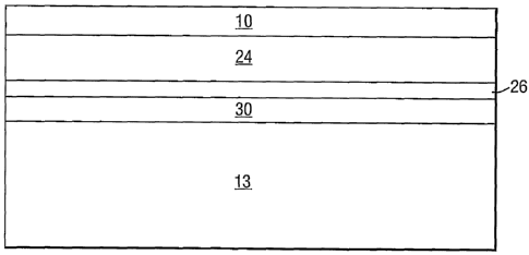
The MOEMS optical modulator shown in Fig. 3a comprises a silicon substrate 13
upon
which is fabricated a layer 30 of silicon oxide, followed by a fixed
polysilicon layer 26.
The fixed polysilicon layer 26 provides the fixed electrode which is separated
from the
moveable micro-mirror 10 by air gap 24. In this embodiment of the invention,
the etalon
comprises a polysilicon-air-polysilicon-oxide-silicon configuration.
In an alternative embodiment shown schematically in Fig. 3b, a dielectric
layer 28 is
provided on top of the fixed polysilicon layer 26. In this embodiment of the
invention,
the etalon comprises an asymmetric polysilicon-air-dielectric-polysilicon-
dielectric-
silicon configuration. The upper polysilicon-air layers provide the tuneable
etalon in
combination with the fixed dielectric layer 28, the polysilicon layer 26, the
dielectric
layer 30 and the silicon substrate 13. The dielectric layer 28 preferably
comprises
silicon oxide, silicon oxy-nitride or most preferably silicon nitride. The
dielectric layer 30
preferably comprises silicon oxide. Alternatively, the dielectric layer 30
could comprise
silicon nitride or silicon oxynitride. In a further alternative, a more
complex structure
could be used with a polysilicon-air-polysilicon moveable upper mirror to
increase the
finesse of the device.
As will be appreciated by the skilled reader, the above-mentioned architecture
may be
fabricated by employing oxide layers which have different relative etch rates
during the
removal of the sacrificial layer, in this case phosphorous doped deposited
silicon oxide.
For example, thermal silicon oxide etches much more slowly in hydrofluoric
acid than
deposited doped oxide layers by a factor of between 5 and 100. However, an
improved
fabrication route is to avoid having exposed silicon oxide layers during a
release etch.
The foregoing embodiments shown in figures 3a and 3b utilise silicon dioxide
as the
dielectric within layer 30 and silicon oxide, silicon oxy-nitride or silicon
nitride as the
dielectric within layer 28, however the skilled person will be aware that
other dielectric
materials may be chosen to give good performance.
Using a dielectric layer 28 in figure 3b confers an addition benefit by
providing electrical
isolation between the polysilicon micro-mirror (used as the upper electrode in
the
device) and the lower polysilicon layer 26 (the lower electrode within the
device). This
configuration facilitates fabrication of an array of optical modulators 2
(where the fixed
polysilicon layer is divided into a plurality of separate electrodes) since
the silicon
CA 02641878 2008-08-01
WO 2007/091053
PCT/GB2007/000414
- 17 -
nitride layer protects the underlying silicon oxide layer from being etched
away during
the process to realise the air gap within the modulator.
Similarly, other structural layers / substrates may be used with appropriate
optical /
mechanical material properties, e.g. polysilicon-germanium, germanium, single
crystal
silicon etc.
An anti-reflective coating (ARC), such as SiO or Ta205/Si02, is typically
added on the
back of the silicon substrate 13 to optimise throughput and reduce the
likelihood of
spurious etalon effects.
To achieve good closed-state performance, a narrow air gap is required (e.g.
30-
100nm) that is challenging without the use of additional stand-off dimples 22
to prevent
large area contacts. One alternative to use the blanket insulating dielectric
layer 28
over the polysilicon electrode (with appropriate optical design) to allow
touching and
define the stand-off. The design is optimized to ensure the moveable micro-
mirror,
overcomes stiction forces and returns to its equilibrium position.
The MOEMS optical modulator according to the present invention enables
operation in
the SWIR, MWIR, LWIR and some parts of the visible spectrum in transmission by
adjusting the gap of the optical cavity.
Optionally, the device is useable in reflection in other optical bands (e.g.
visible)
provided sufficient travel is allowed (defined by the gap). Optionally, a thin
upper
reflective coating is used to improve performance.
Digital operation of the optical modulator is sufficient, in which case the
micro-mirror is
positioned either in its upper equilibrium position, or in its lower position
in close
proximity to the lower fixed electrode. The upper equilibrium position and the
lower
position shall. include those positions adopted by the mirror with a reference
voltage Vref
applied to the modulator. The modulator is preferably used in transmission
rather than
reflection to improve system design. When used as a transmissive modulator,
the
optical modulator substantially blocks transmission of electromagnetic
radiation there-
through when the micro-mirror is positioned in its upper equilibrium position
and
CA 02641878 2008-08-01
WO 2007/091053
PCT/GB2007/000414
- 18 -
substantially transmits electromagnetic radiation there-through when the micro-
mirror is
positioned in its lower position in close proximity to the substrate.
The present MOEMS modulator is particularly applicable to MWIR and SWIR
imaging
applications where other conventional modulator solutions cannot be applied
for
reasons of performance (e.g. LCD) or cost (e.g. multi-quantum well devices).
Moreover, since the modulator may be fabricated exclusively from silicon,
thermal bi-
material effects are reduced or eliminated, and hence the behaviour of the
modulator is
largely unaffected by operational temperature (e.g. ranges in excess of -40 C
to +70 C
are readily accessible). This means that is suitable for cooling so that the
micro-mirror
does not add noise to an image. Accordingly, the modulator may be
advantageously
employed in IR imaging applications and adaptive coded aperture imaging
applications
(AC IA).
Figures 4a to 4c show typical performance characteristic for the tuneable
cavity of Fig.
3b. Specifically, Fig. 4a shows transmittance in the MWIR waveband for the
optical
modulator when the micro-mirror is in its upper equilibrium position and in
its lower
position at normal incidence. Fig. 4b shows transmittance against MWIR
waveband for
the optical modulator when the micro-mirror is in its upper equilibrium
position and in its
lower position for incident angles of 0 degrees and 50 degrees. Fig. 4c shows
transmittance against angle of incidence by polarisation. In practice,
incident angles in
the range 15 degrees to 20 degrees may be used to minimise angular effects. In
situations involving modulation of radiation from the atmosphere, it is
beneficial to
arrange transmission peaks to coincide with atmospheric transmission windows.
The dimensions of the. optical stacks within the etalon may be optimised
across the
spectral and angular range to maximise contrast ratio ¨ moving away slightly
from
conventional half/quarter wave optical stacks for a single wavelength device.
Fig. 5a shows a typical performance characteristic for the tuneable cavity of
Fig. 3b
optimised for maximum transmission in an optically open state in the 3.5pm to
4.5pm
waveband using the following layer sequence:
polysilicon micro mirror-air-silicon nitride-polysilicon-silicon dioxide-
silicon substrate.
CA 02641878 2014-01-07
31158-41
- 19 -
In this particular embodiment, the two states of the optical modulator
(optically open ¨
substantially transmissive / optically closed ¨ optically non-transmissive)
are achieved
by moving the micro-mirror so as to adjust the air gap in the modulator.
Standard
positions would be ¨1pm and ¨50nm .
For specific imaging applications, e.g. adapted coded aperture imaging (ACAI),
it is
desirable to produce a two-dimensional array of MOEMS optical modulators
wherein
each optical modulator is individually addressable. This enables individual
optical
modulators within the array (also referred to hereinafter as picture elements
or pixels)
to be set in the optically closed or optically open position (reflect '0" or
transmit "1"). For
example, see figure 5b which shows a schematic representation of an adaptive
coded
aperture imaging (ACAI) system, including a two-dimensional array of MOEMS
optical
modulators according to an embodiment of the present invention.
=
Hence, according to another embodiment of the present invention, a spatial
optical
modulator comprises a two dimensional array of optical modulators of Figs. 1
to 3
addressable using a passive matrix row / column addressing scheme without the
need
for sub-pixel control electronics that would reduce fill factor unacceptably
in a
transmissive device. A critical aspect for the transmissive architecture is
that the lower
electrode is transparent and part of the optical design. A key benefit is that
this
embodiment of the invention enables a MEMS-only chip to be addressed using an
off-
chip drivers and means an integrated MEMS process is not necessary. This
approach
enables separate optimisation Of the MEMS architecture and the pixel control
electronics, reduces costs and provides a two-dimensional array which is
scaleable to
any size. = . .
Passive matrix addressing of the two dimensional array is achieved in this
embodiment
of the invention by making the constituent optical modulators bistable using
appropriate
voltages.
In order to achieve this bistable characteristic, the micro-mirrors are
arranged such that
when the voltage applied to the optical modulator exceeds a certain value, the
micro-
mirror will snap down from the equilibrium position to the 'pull in' (or
'latch down')
CA 02641878 2008-08-01
WO 2007/091053
PCT/GB2007/000414
- 20 -
position. Non-linear effects in MOEMS optical modulators have hitherto been
considered to be detrimental to the operation of the device and efforts have
been made
to eliminate such effects, for example see patent US 5,838,484 which describes
a
MOEMS optical modulator with linear operating characteristic.
Accordingly, in the present invention each optical modulator 2 within the
array is
arranged so that the micro-mirror 10 therein will only latch down (pull in)
when the
applied potential difference across a pair of electrodes exceeds a threshold
voltage
(Vpi), in which condition the electrostatic attraction force is greater than
the mechanical
restoring force provided by the supporting springs 14. The optical modulator
exhibits
hysteresis so that the pull off voltage (Vpo) is significantly lower than the
pull in voltage.
The degree of hysteresis may be tailored by appropriate design.
In order to enable passive matrix addressing, the pull off (or release)
voltage is
arranged to be significantly lower (e.g. a factor of 2) than the pull in
voltage. See for
example Fig. 6 which shows schematically the hysteresis characteristic of one
of the
optical modulators within the array of the present embodiment.
In the present embodiment, the two dimensional array of optical modulators are
arranged in a matrix between a plurality of column address electrodes 32, and
a
plurality of underlying row address electrodes 34, see Fig. 7. The upper
column
address electrodes 32 comprise the moveable micro-mirrors 10 within the
optical
modulators whereas the row address electrodes 34 comprise the fixed electrode
plate
36 in each optical modulator and accessed via the edge, Fig. 7b refers.
Figure 7c shows a schematic cross-sectional representation of another
embodiment of
the invention comprising an encapsulated two dimensional array of optical
modulators.
Here, the optical modulator array is enclosed by a cap 31 attached using a
wafer / chip
scale encapsulation technique to the substrate 13 by a bond layer 29. In
figure 7c, the
cap is has a rebate formed therein. Alternatively a planer cap may be used if
the
thickness of the bond layer 29 is increased accordingly. Encapsulation in this
manner
enables the pressure within a sealed device to be controlled, thereby allowing
the
mechanical damping of the micro-mirrors to be controlled. This technique
simplifies
processing as devices are released wafer scale, bonded and sawn ¨ avoiding
debris
issues and simplifying, handling during packaging / integration into system.
The cap 31
CA 02641878 2008-08-01
WO 2007/091053
PCT/GB2007/000414
- 21 -
is provided with appropriate antireflection (AR) coatings and an appropriate
spacing to
the moveable mirror (e.g. > coherence length of light in application to avoid
unwanted
etalon effects). This spacing may be achieved by a rebate in the cap (as shown
in the
figure) and/or a bond spacer between the modulator wafer and the cap wafer. It
is
possible to actively use the gap between upper cap 31 and moveable mirror 10
in
some way to further tune optical performance and exploit etalon effects with
small gap.
Through wafer vies could also be incorporated into the substrate or cap (or
even the
electronic chips) to enable direct mounting of the electronic driver chips
without flipping.
Optionally, the cap may be shaped to provide an element or elements having an
optical
functionality or optical power, for example the cap may have a lensing
function.
In the present arrangement, the voltage applied to a given optical modulator
within the
array is the sum of the voltage applied to the moveable micro mirror (the
column
voltage) and the voltage applied to the fixed electrode (row voltage). This
configuration
enables each optical modulator or pixel within the array to be set
individually in a row /
column address scheme.
An addressing scheme according to one embodiment of the invention is now
described
which enables each pixel to be set and reset individually in a row / column
addressing
scheme (the whole array does not need to be reset to unlatch a pixel).
Those skilled in the art will appreciate that there are other ways of changing
the column
/ row voltages to achieve the same functionality of moving the net potential
difference
applied to each pixel to fall within the hysterisis zone (hold), below the
pull off voltage
(reset) or above the pull in voltage (set) as described in detail herein. For
example,
during the reset function, the voltage of the column containing mirrors to be
reset needs to be lower than that of the other columns such that the sum of
the column
voltage and the row voltage falls below the pull-off voltage. This may be
achieved by
reducing the voltage of the column of interest below the reference voltage
(such that
Vref - Vreset > Vp0 for other columns) or by increasing the voltage of the
other columns
above the reference voltage by Vse}2 such that their potential remains above
the pull off
voltage whilst the column of interest (at Vref) in conjunction with the row
voltage fall
below the pull off threshold. Similarly, the row and column voltages could be
CA 02641878 2008-08-01
WO 2007/091053
PCT/GB2007/000414
- 22 -
interchanged such that rows would be sequentially addressed whilst all the
columns
are set in parallel.
The addressing scheme according to the present embodiment of the invention is
based
on electrostatic hysteresis (see Fig. 6) where Vo is the latch (pull in)
voltage and Vp0 is
the release (pull off) voltage. With reference to the prior art, the
addressing scheme of
EP 1 341 025 resets the entire modulator array by removing the latch voltage.
EP 1
341 025 also uses a separate latch electrode. This makes only changing small
parts of
the array, whilst leaving the remainder unaffected, difficult and is
potentially inefficient
(requiring higher addressing speeds to adapt the array pattern in a given
time).
The addressing scheme described in this embodiment is best illustrated by the
sequences shown in Fig 8. Referring to Fig. 8, the row location is denoted by
R row
no., the column location by C column no. and pixel location by P row no.,
column no.
For this example, let Vo = 14V, Vp0 = 10V. The upper graph in Fig. 8 denotes
row
voltage states (e.g. up = -2V (-Vr0w_sef), down = +2V (Vrow_set), centre = OV)
and column
voltage states (e.g. up = 13V (Vref+Vset), centre = 11V (Vref) and down = OV).
The drive
voltage for a given pixel is given by (Vcolumn Vrow). The lower graph in Fig.
8 denotes
whether a given pixel is in latched (1) or released (0) state. The voltages
used here are
typical of a 25pm micro-mirror with a 1.2pm gap designed to modulate in the
SWIR at
100kbps.
The operations are performed by setting the appropriate combination of
voltages as
follows:
Set pixel ¨ all columns at hold voltage reference, Vref, except column with
pixels to be
set at Vref + Vset < =Vpi. Row voltages with pixels to be latched set to -Vrow-
set so that
potential difference, Vref + Vset Vrow-set > Vpi (other columns at Vref + Vrow-
set < Vpi so do
not latch). Vrow-set removed from row and all columns returned to Vref to hold
pixels in
latched state.
Reset pixel ¨ all columns at Vref + Vset (Wpi) except column with pixels to be
reset
(released) at \fret. Row voltages with pixels to be released set to +Vreset so
potential
difference across pixels is Vref¨ Vreset <V0 (other columns at Vref + Vset
¨Vreset > Vpo 50 if
CA 02641878 2008-08-01
WO 2007/091053
PCT/GB2007/000414
- 23 -
latched remain so). Vreset removed from rows and all columns returned to Vret
to hold
desired pixels in latched state.
Reset/Set all ¨ All columns to OV to reset all. All columns to Viet Vset and
all rows to
Vrow-set to set all.
A complete column may be addressed in parallel in this way (i.e. all the row
voltages
are set to change the entire column when the column voltage is set. Columns
are
addressed sequentially.
The terms row and column used above are not limiting but may be interchanged
without affecting the addressing scheme.
In principle, using this approach the spatial optical modulator array is
scaleable to any
size. For an imaging scenario, the individual pixel micromirror pitch is
likely to fall in the
range 15-100pm. When used in an imaging application, preferably the pitch
matches
the pitch of pixels in the imaging array of the detector. The array must
,comprise
independent columns and, in practice, the size will be limited by resistance /
capacitance (RC) time constant considerations. This is mitigated by only
switching one
column at any time. The resistance of individual pixels will be dominated by
the spring
width and length ¨ for example, in 0.5pm thick polysilicon with a 2pm spring,
the pixel
array resistance is of the order of 500K0/cm whilst the capacitance of the
array is of
the order of 50pF/cm (for a 100pm pixel plate) giving an RC constant of
2.5ps/cm. A
stepper field size as used in lithography is typically of the order of 2x2cm
and so this
would be a practical size limit for a tile to build up larger arrays whilst
maintaining good
control and yield. However, employing a buried layer or a second layer of
lower
resistance polysilicon interconnect above the spring could reduce the
resistance
significantly (>10x). Alternatively or additionally, a thin metal layer could
reduce track
resistance by 2-3 orders of magnitude if speed / resistive voltage drop is an
issue. For
example, this could be deposited when the device is partially released using a
combination of shadow masking from the structure itself and/or lift-off to
protect areas
where no Au is required (e.g. transmissive region of pixel). Where the
modulator
comprises additional polysilicon and metal conductor, layers, said layers may
be
arranged to form an optically blocking layer in parts of device to maintain
optimal
contrast. This is particularly beneficial in low fill factor devices.
CA 02641878 2008-08-01
WO 2007/091053
PCT/GB2007/000414
- 24 -
For the electrode layer, the fixed polysilicon acts as the electrical conduit.
This is
significantly wider than the spring in the moveable array layer and so less
likely to limit
performance. To reduce its resistance further, the electrode array could be
connected
to the substrate with implanted tracks periodically using vies. The tracks in
the
substrate are isolated using reverse biased pn diodes as a result of the
implants. For
the most aggressive resistance control, a silicide or metal tracks could also
be defined
on the substrate but care would be needed that it did not interfere with the
optical path.
A metal-nitride process is an interesting alternative in this circumstance as
both the
electrode and moveable micro mirror layer would contain low resistance metal
tracking.
The drive voltage would likely be higher due to the need to fabricate the
majority of the
micro mirror as PECVD nitride only to allow transmission (unless an IR
transmissive
metallization were employed). In practice, metallization may applied to the
top and the
bottom of the PECVD nitride layer so as to reduce thermal bi-material effects
and to
reduce the drive gap (thereby reducing the drive voltage).
Optionally, a micro-lens array may be used in conjunction with the spatial
optical
modulator of the present invention to maintain the efficiency of the optical
modulator in
circumstances where the fill factor of modulators within the spatial optical
modulator
array is reduced. ,
According to further embodiment of the invention a process of optical
apodization can
be used within the present spatial optical modulator to reduce edge effects
and hence
diffraction. The pixel can be apodized by suitably profiling one of the cavity
mirror
elements within the optical modulators of the array. For example, the mirror
may be
imparted with a monotonically increasing profile, a stepped profile etc
designed so as
to reduce the optical transmission of the individual Fabry-Perot elements.
Most
practically, this would be constrained to near the periphery of the micro
mirror.
Alternatively, or in addition, to achieve apodization, metallization is added
to the
edge(s) of the cavity mirror. The metallization may comprise a layer or layers
of metal
(e.g. gold). The thickness of the metallic layer may be graduated. In
addition, or
alternatively, the metallization is applied using a grey scale pattern (half-
tone pattern)
etc. to vary the optical density of the metallic layer.
CA 02641878 2008-08-01
WO 2007/091053
PCT/GB2007/000414
- 25 -
In terms of MEMS design, the main features of interest are the speed, voltage
(power)
and micro mirror size. With reference to the figures, Fig. 9a shows a plot of
predicted
resonant frequency vs. pixel thickness, Fig. 9b shows a plot of predicted
resonant
frequency vs. plate size, Fig. 9c shows a plot of predicted drive voltage vs.
plate size,
__ and Fig. 9d shows a plot of predicted fill factor vs. plate size. Figs. 9a
to 9d highlighting
the following trends; larger pixels reduce the drive voltage and increase the
fill factor
whilst reducing speed, the four spring design is faster but requires a larger
drive
voltage and has a lower fill factor, thinner pixels reduce the drive voltage
and the
speed.
It will be appreciated by the skilled person that large areas can be tiled
from smaller
MOEMS spatial optical modulator arrays according to the present invention. In
another
embodiment of the invention hybrid integration employing direct chip attach
techniques
is used to flip and bond a thinned driver electronics chip 40 onto two sides
of a
MEOMS spatial optical modulator array chip for column and row addressing
respectively (e.g. using fine geometry solder bump technology). When scaled to
a two
dimensional array of tiles (modulator chips), this results in a MEMS chip
surrounded on
all 4 sides by driver chips. A dummy chip may be used for the blank edges
around the
periphery of the tile array. The driver chips may alternatively contain
electronics for two
__ neighbouring chips, requiring a driver chip on a 4 edges of every tile.
Using this
technique, two MOEMS modulator chips are attached by each electronics chip as
shown in Figure 10.
Building large arrays out of small tiles is the most effective way to reduce
cost as yield
__ deceases with chip area. It also controls the number of columns and rows
each driver
chip needs to address (and hence RC / resistive loss and power/current
considerations). For,example in a 2x2cm chip, if the pixel pitch were 20pm,
there would
be 1000 rows and 1000 columns. This requires 10 bit addressing. Such as chip
could
be realised in a 0.35pm mixed CMOS technology if the drive voltage were below
3.3V
__ or 0.8pm mixed CMOS technology if the drive voltage were below 5V. Higher
drive
voltages would require a high voltage (20 ¨ 50V) process variant and / or
larger
geometry process, resulting in a highly specialised design of drive
electronics.
Transistor sizes in high voltage processes are also larger, meaning that this
approach
may cease to be viable using simple layouts and architectures. Configurations
using
__ combinations of driver chips operating at different drive voltages are also
feasible. For
CA 02641878 2008-08-01
WO 2007/091053
PCT/GB2007/000414
- 26 -
example in a column and row addressing scheme, the column address driver may
comprise a standard CMOS driver chip, whereas the row address driver may
comprise
a high voltage driver chip. In this example, the high voltage driver chip is
capable of
operating up to 40v for small pixel pitches.
Using such a tiling arrangement, it is also possible to realise non-flat
shapes, such as a
geodesic dome to give added rigidity. Figure 10 also illustrates an optional
support
frame which has elements 42 arranged to increase the rigidity of the tiled
array. The
support frame may advantageously be thermally conductive (e.g. metallic) and
may be
used to control the temperature of the tiled array. For example, the whole
array may be
cooled by removing heat from the edges via the support frame. Optionally, the
support
frame comprises a hollow cross-section through which a cooling fluid is
passed.
Alternatively, the data and /or power connections may be routed through or on
the
support frame to the tiled plurality of MOEMS arrays.
A 50x50 array of 2cm chips may be further multiplexed to enable/disable a
particular
chip for setting and give a 1x1m mask. If using a single element, this would
require 16
bit addressing on a 2.5Gpixel array.
The speed to update a tiled large area array is a major design consideration.
The
voltage drives a capacitive load and so the electrical speed is limited by RC
considerations. For a typical design, the RC time constant is of the order of
2.5ps/cm
length ¨ compatible with a 10ps/pixel switching speed for a 2x2cm chip. In the
above
configuration, this is limited by the resistance of the polysilicon in the
column path and
to a lesser extent the rows. Both could be reduced by adding a more conductive
path
in parallel with a slight addition in process complexity as previously
described. The
mechanical response is determined by the resonant frequency of the device and
the
damping (pressure). The frequency is dependent on the thickness of the moving
layer,
the spring design and the pitch. With appropriate design, it is predicted to
be of the
order of 1-10ps. With potentially a 1000x1000 array (20p,m pitch on a 2cm
chip), an
array update time of below 10ms results using the addressing scheme proposed
herein
wherein pixels within a whole column are set in parallel. By using tiles of
this size, and
driving / addressing all modulator tiles in parallel, an array of any size may
be set at the
same speed as an individual tile.
CA 02641878 2008-08-01
WO 2007/091053
PCT/GB2007/000414
- 27 -
The drive voltage depends on the pixel area, spring geometry and gap. For an
optical
design with a 35pm pixel, it is of the order of 5V and it would be capable of
responding
at up to 200kHz. Power consumption is a function of the voltage in combination
with
the capacitance, number and frequency of pixels changing states and the
efficiency of
any charge recovery schemes employed.
The MOEMS optical modulator according to any of the foregoing embodiments of
the
present invention is fabricated by successive depositing of material layers on
a silicon
substrate. Alternatively the device is manufactured using the device layer of
a SOI
wafer that is patterned and transferred to the MEMS wafer in place of the
polysilicon
structural layer. This could be advantageous as high temperature processing
steps
would not be required to control the stress in the polysilicon layer and
enable
conventional CMOS electronics on the substrate.
It is possible to post-process the present MOEMS optical modulator on a
substrate
containing CMOS using a low temperature technology, such as polysilicon-
germanium
micromachining (e.g..IMEC or UC Berkeley) or a metal-nitride process (e.g.
QinetiQ).
The latter would use a PECVD nitride film as the main optical/structural
element with
low resistance metal tracking as previously described. It is also possible to
incorporate
the standard polysilicon process into a modified large geometry (2-3pm) CMOS
or
BiCMOS process flow with slightly degraded transistor characteristics.
One particular application of the MOEMS spatial optical modulator array of the
present
invention is as a reconfigurable mask within an adaptive coded aperture
imaging
(ACAI) system. Referring to figure 5b, the reconfigurable mask comprising at
least one
of the present MOEMS spatial optical modulator arrays is used in front of a
two-
dimensional detector array and arranged to modulate the amplitude and / or
phase of
electromagnetic radiation incident thereon from a scene. The mask provides a
plurality
of individually addressable apertures or pin-holes.. Typically the pitch of
apertures
within the mask is ^15 - 50pm. In practice, a plurality of optical modulators
may be
grouped together to act as a larger modulator having a greater effective
aperture. For
example, four individual optical modulators each having a 50pm2 sub aperture
may be
grouped to form a single optical modulator having a 200pm2 effective aperture.
CA 02641878 2008-08-01
WO 2007/091053
PCT/GB2007/000414
- 28 -
Alternative applications of a MOEMS spatial optical modulator of the present
invention
include, but are not limited to, in-use calibration of infrared detector
arrays, electro-
optical protection and scanning detector applications.
Calibration of infrared detector arrays is an important application of the
present
MOEMS spatial optical modulator since, due to variations in the manufacturing
process, the output signal from an infrared detector varies considerably from
detector
to detector. This is true even in a two-dimensional array of detectors made at
the same
time. Individual elements on a two-dimensional array of infrared detectors are
normally
accessed by bump bonding the array on to a silicon readout circuit which can
act as a
multiplexer. Variations in the properties of the silicon transistors add to
the variation in
the outputs and in general make the output vary non-linearly with input flux.
It is therefore essential to calibrate the output from each pixel in an array
as a function
of flux. Due to the non-linear nature of the variation, it is necessary to do
this.calibration
at a significant number of fluxes if high quality imaging is needed over a
range,,of scene
temperatures (such as viewing sky and ground).
The conventional solution is to use a thermo-electrically controlled
calibration black-
body plate and measure the output as a function of the plate temperature. The
disadvantage of this technique is that allowing for settling time at each
temperature it
can take up to seven minutes to complete this procedure. Ideally a source is
required
which can produce a stable range of fluxes rapidly. As well as reducing the
time-to-
operation, this will enable more frequent calibration cycles. This will help
reduce drift in
the calibration settings due to effects such as variation in the array
temperature.
Furthermore, since silicon and polysilicon have the same temperature
coefficient of
expansion, heating and cooling does not add additional stresses in the spatial
optical
modulator which may otherwise adversely effect performance.
A fast calibration source may be produced by combining a conventional fixed
temperature black-body plate and a reconfigurable adaptive coded aperture
(ACA)
mask comprising a MOEMS spatial optical modulator according to the present
invention. As before, the ACA mask consists of an array of openings in a mask
plate
which can be opened or closed to vary the flux falling on the detector.
Ideally, the ACA
=
CA 02641878 2014-01-07
31158-41
- 29 -
=
mask would be cooled, however this may not be necessary if the switching goes
from a
transmissive to a reflective state.
A range of calibrated fluxes can be generated by varying the number of
openings from
fully closed to fully open. As switching of the mask can be done relatively
quickly, it
should be possible to get multipoint calibrations in a short time. A possible -
configuration of a camera using this system is shown in figure 11. The
infrared camera
system 50 of figure 11 employs an ACA mask 52 arranged on a paddle and a
thermo-
electrically (TE) controlled black body plate 54 arranged on a paddle. During
calibration, the ACA mask 52 and the TE controlled plate are rotated by
rotation means
56 into a position between the camera lens 58 and the two-dimensional infrared
detector array. During calibration, the two-dimensional infrared detector
array images
the thermo-electrically (TE) controlled black body plate 54 rather than
receiving infrared
radiation from a scene outside the camera. For a conventional imaging system,
the
mask is not at an imaged position and hence the illumination of the focal
plane will be
uniform ¨ however this can be improved by spreading out the openings uniformly
on
the ACA mask.
In an adaptive coded aperture imaging (ACAI) system as described above, an ACA
mask is already included and hence the abovementioned calibration scheme can
be
implemented without additional cost. A particular application is in a lens-
less adaptive ,....
coded aperture imaging (ACM) system. In a lens-less ACAI imaging system, the
flux
falling on each detector is expected to be relatively uniform (due to
averaging flux from
all the openings) and good imaging will depend on accurate calibration over a
relatively
small range of flux. A range of fluxes around this value could again be
generated by
opening different patterns on the mask. A more complex scheme may be
implemented
which can calibrate out variations in the transmission of the individual
openings on the
mask.
In view of the foregoing description it will be evident to a person skilled in
the art that
various modifications may be made within the scope of the invention, and the
scope of the
invention is not limited to the specific embodiments described above.
. .