Note: Descriptions are shown in the official language in which they were submitted.
CA 02642309 2008-10-29
CHECK AND OTHER ITEM DESIGN FOR REFLECTANCE VALUES
DETERMINATION PRIOR TO ITEM MANUFACTURE
FIELD OF INVENTION
[0001] The present invention relates to item image quality verification.
BACKGROUND
[0002] The current paper document-processing environment is dependent upon
paper
processing, which can be inefficient. What is needed is an efficient
electronic paper document
design process that confirms a paper document design that will be compatible
with current
electronic capture, storage, and processing system, which are used to
alleviate or otherwise
mitigate the dependence upon paper form of items such as personal and business
checks, for
example. Since a vast majority of checks are transported physically via air
from one bank to
another, and planes can be grounded for a variety of reasons, substantial
costs can be incurred by
banks due to check processing being delayed. The current system relies upon
the physical
movement of original paper checks from the bank where the checks are deposited
to the bank
that pays them, which can be inefficient and costly.
100031 Under current law, a bank may send the original paper check for payment
unless it has
an electronic payment agreement with the paying bank. Under Check 21
legislation in the United
States, by authorizing the use of a new negotiable instrument called a
"substitute check" (aka
image replacement document), electronic check processing is enabled without
mandating that
any bank change its current check collection practices. The substitute check
is a paper
reproduction of an original check that contains an image of the front and back
of the original
check, which is suitable for automated processing in the same manner as the
original check, as
long as the check image meets other technical requirements, such as having
mandated image
quality, otherwise referred to as image readiness.
[0004] As a result of Check 21, banks that wish to scan the original paper
check to create a
substitute check will require it to be "image ready" compatible. Image
readiness is the design
attributes of a check that ensures optimum recognition of amounts, legibility
of handwriting, and
reasonably low file size. Current testing of image readiness procedures uses a
scanner to convert
a physical check into a binary image, which is then analysed to ensure that
the entire check
TOR_LAW\ 6985922\1 - 1 -
CA 02642309 2008-10-29
background of the resultant image scan is Check 21 compliant. The testing is
performed to
ensure minimal background clutter and high background reflectance. For
example, excessive
background clutter causes interference with the legibility of handwritten data
and low
background reflectance causes handwritten data to drop out due to insufficient
contrast.
Background clutter can consist of offset ink that does not drop out when
scanned, which causes
the background features of the document to remain in the document image.
[0005] Unfortunately, current testing is only used to test compliance of the
final version of
check document designs, which is extremely inefficient since the current
design process is
heavily manual in nature, requiring the cyclic iteration of offset press setup
and printing and then
final testing of the resultant physical draft check version. In the check
design process, design
features that are desirable to the naked eye are not always compatible from a
imaging quality
exhibited by a physical paper document. This manual design process is
inefficient in cost and
time due to the multiple check versions that must be physically manufactured
in order to finalize
a check design that ultimately satisfies current image readiness standards.
[0006] Current check designs have to be printed and then tested for image
readiness in order
to confirm how a typical reader/sorter will process the resultant image of the
check. If the
physical check design is rejected by a reader/sorter, them modifications are
required and the
check design is adjusted and a new physical check is printed for image
testing. It should be noted
that a new plate, for an offset printing process, is created for each new
check design, which is
considered an expensive and time consuming process. What is needed is a
system/method for
predicting the image quality of a physical check or other image-ready item
before the check of
other image ready item is manufactured.
SUMMARY
[0007] There is a need for a method and a system for item design that
overcomes or
otherwise mitigates a disadvantage of the prior art.
[0008] Current check designs have to be printed and then tested for image
readiness in order
to confirm how a typical reader/sorter will process the resultant image of the
check. If the
physical check design is rejected by a reader/sorter, them modifications are
required and the
TOR_LAW\ 6985922\1 - 2 -
CA 02642309 2008-10-29
check design is adjusted and a new physical check is printed for image
testing. Contrary to
current systems and methods there is provided a system and method for
determining a plurality of
reflectance values for an item design representing a physical item having at
least one area of
interest on a surface of the physical item for containing critical data and a
background feature
positioned on the surface, the physical item suitable for positioning in a
digital image capturing
device, the system comprising: an input module configured for receiving one or
more material
reflectance values of a substrate for providing said surface and design
parameters for said
background feature, the design parameters including a color and a print
density of said
background feature; a memory configured for storing a plurality of color
reflectance values
assigned to a corresponding plurality of selected combinations of specified
design parameters; a
look-up module configured for determining from the memory one or more color
reflectance
values having the specified design parameters matching the design parameters
for said
background feature; a combination module configured for combining the one or
more material
reflectance values with the corresponding one or more color reflectance values
to produce
resultant one or more design reflectance values representative of the
reflectance of physical item
when having the background feature positioned on said surface of the
substrate; wherein the one
or more design reflectance values of the item design are for use in
determining whether the
design parameters would produce the physical item having an acceptable digital
image when
processed by the digital image capturing device.
[0009] One aspect provided is a system for determining a plurality of
reflectance values for
an item design representing a physical item having at least one area of
interest on a surface of the
physical item for containing critical data and a background feature positioned
on the surface, the
physical item suitable for positioning in a digital image capturing device,
the system comprising:
an input module configured for receiving one or more material reflectance
values of a substrate
for providing said surface and design parameters for said background feature,
the design
parameters including a color and a print density of said background feature; a
memory configured
for storing a plurality of color reflectance values assigned to a
corresponding plurality of selected
combinations of specified design parameters; a look-up module configured for
determining from
the memory one or more color reflectance values having the specified design
parameters
TOR_LAW\ 6985922\1 - 3 -
CA 02642309 2008-10-29
matching the design parameters for said background feature; a combination
module configured
for combining the one or more material reflectance values with the
corresponding one or more
color reflectance values to produce resultant one or more design reflectance
values representative
of the reflectance of physical item when having the background feature
positioned on said
surface of the substrate; wherein the one or more design reflectance values of
the item design are
for use in determining whether the design parameters would produce the
physical item having an
acceptable digital image when processed by the digital image capturing device.
[0010] A further aspect provided is a method for determining a plurality of
reflectance values
for an item design representing a physical item having at least one area of
interest on a surface of
the physical item for containing critical data and a background feature
positioned on the surface,
the physical item suitable for positioning in a digital image recorder, the
method comprising:
receiving one or more material reflectance values of a substrate for providing
said surface and
design parameters for said background feature, the design parameters including
a color and a
print density of said background feature; accessing a plurality of color
reflectance values
assigned to a corresponding plurality of selected combinations of specified
design parameters;
determining one or more color reflectance values having the specified design
parameters
matching the design parameters for said background feature; combining the one
or more material
reflectance values with the corresponding one or more color reflectance values
to produce
resultant one or more design reflectance values representative of the
reflectance of physical item
when having the background feature positioned on said surface of the
substrate; wherein the one
or more design reflectance values of the item design are for use in
determining whether the
design parameters would produce the physical item having an acceptable digital
image when
processed by the digital image capturing device.
BRIEF DESCRIPTION OF THE DRAWINGS
[0011] These and other features will become more apparent in the following
detailed
description in which reference is made to the appended drawings by way of
example only,
wherein:
[0012] Figure 1 is an exam item as a check;
TOR_LAW\ 6985922\1 - 4 -
CA 02642309 2008-10-29
[0013] Figure 2 shows example areas of interest of the item of Figure 1;
[0014] Figure 3 shows an image of the item of Figure 1 with background
features removed;
[0015] Figure 4 shows example occlusion of critical data as a result of
reflectance
inteRberence between the critical data and background features on the item
surface;
[0016] Figure 5 shows an example item design environment;
[0017] Figure 6 shows a block diagram of an example operation of the item
design
environment of Figure 5;
[0018] Figure 7 shows an example combination of reflectance values for the
design
environment of Figure 5;
[0019] Figure 8 shows an example embodiment of a computing system item design
environment of Figure 5;
[0020] Figure 9 shows an example portion of an assigned reflectance map for
the design
image of Figure 1;
[0021] Figure 10 shows an example relationship between a perceived colour of a
colour scale
and its corresponding reflectance value for use in determining the assigned
reflectance values of
the reflectance map of Figure 9; and
[0022] Figure 11 is an alternative embodiment of the reflectance map of Figure
9
DESCRIPTION
Items 12
[0023] Referring to Figure 1, shown are two example physical items (e.g.
checks) 12 having
a plurality of areas of interest (AOIs), see Figure 2, which are considered as
the areas on an item
surface 13 that contain critical data 15 (e.g. signature) that should be
discernable in a recorded
digital image 17 of the item surface 13 (see Figure 3). In the case of where
the physical item 12
is a check, the areas of interest AOI are such as but not limited to: Date;
Payee; Numerical
Amount; Legal Amount (Amount Spelled out); Signature Lines; and the MICR
numbering line
Area. In general, It is noted that the areas of interest AOI also contain
background features 18
(e.g. pictures/images, designs, fill schemes, personal or business logo; font
style; color; size and
location background features and check fields - e.g. AOIs, etc.). These
background features 18
TOR_LAW\ 6985922\1 -5-
CA 02642309 2008-10-29
(e.g. design parameters 14 define a plurality of background features 18
positioned on the surface
13) must be designed such that they provide a desirable graphical design
appeal of the item
surface 13 while at the same time do not occlude or otherwise interfere with
the quality of the
digital image recording of the critical data 151ocated in the areas of
interest AOI. It is
recognised that the image capturing process of the item surface 13 provides
for the conversion of
the item surface 13 via scanning and binary conversion (i.e. into a plurality
of pixel values) of the
critical data 15 (e.g. handwriting) from the areas of interest AOI.
[0024] It is recognised that the physical items 12 can be manufactured using a
variety of
different stock materials 16 (see Figure 5) such as but not limited to paper,
plastic, etc. It is also
recognised that the physical items 12 can be embodied as any item that has a
requirement for
image quality of selected areas (e.g. AOIs) of the item surface 13, such that
the selected area(s)
AOI(s) of an image 17 (e.g. scanned), see Figure 3, of the physical item 12
satisfy specified
reflectance threshold(s) 20 (see Figure 5). Examples of the physical items 12
are such as but not
limited to: checks; coupons; forms; credit cards; debit cards; loyalty/reward
cards; and other
items 12 suitable for having the image 17 (e.g. a grey scale image converted
to a binary image)
captured of the item surface 13 (e.g. front side and/or backside of the
physical item 12).
[0025] Referring to Figure 2, shown are example areas of interest AOI for a
check
embodiment of the physical item 12, as discussed above. It is also recognised
that the areas of
interest AOI for a credit and/or debit card can be areas such as but not
limited to: signature
region, card number, visible biometric information; other visible security
feature positioned on
item surface 13; logo or other visible icon(s); etc. Referring to Figure 3,
shown is the digital
image 17 of the physical item 12 of Figure 1, such that the background
features 18 (see Figure 1)
have not occluded the critical data 15 resident in the areas of interest AOI.
Reflectance
[0026] Low background reflectance causes low contrast and unintended dropout
of vital
information (e.g. critical data 15), while high contrast background patterns
18 cause random
background clutter to remain in the binary images 17 that renders critical
data 15 (e.g.
handwriting) ambiguous at best.
TOR_LAW\ 6985922\1 -6-
CA 02642309 2008-10-29
100271 Currently in the art, background clutter can be measured by creating
the image 17 of
the physical item 12 (e.g. without any critical data 15 input into the blank
AOIs) that contains the
AOIs, then converting the image 17 from gray scale to black-and-white (e.g. a
binary image)
using a standardized conversion process as is known in the art, and then
measuring the clusters of
black pixels (paxel count) which remain after conversion.
[0028] As part of standardized image 17 quality for physical items 12,
specifically the
requirements (e.g. ANSI) focus on the areas of interest AOI for background
drop out, such that
the background features 18 will not occlude or otherwise adversely affect the
image quality of the
critical data 15 resident in the areas of interest AOI. For example, in
standardized image quality
testing for physical items 12, this testing is done by measuring a paxel 21
count in a pre-
determined area, see Figure 4, in order to determine the legibility of
handwritten data or other
critical data 15. The paxel 21 can be defined as "a group of dark (e.g. black
in the case of grey
scale images 17) pixels 23 in a binary image 17 measuring a certain specified
dimension (e.g.
.010" x .010" square), which is the smallest dark area of background clutter
caused by visual
interference of the critical data 15 with the background features 18 in the
image 17 considered to
affect the legibility of the critical data 15 of the physical items 12 when
scanned. A related term,
"paxel 21 count" refers to the number of contiguous paxels 21 that, when
joined in any shape,
line or combination (e.g. string 22) can create a background clutter problem
to affect the
legibility of critical data 15 on the image 17. A standard definition for a
paxel is a group of black
pixels (equal to or more than 6 of 9) in a binary image, measuring 0.010 inch
x 0.010 inch
(0.25mm x 0.25mm) square, that is the smallest dark area of background clutter
that has been
determined to affect the legibility of handwritten data on checks.
[0029] As mentioned above, the paxels 23 are formed in the image 17 through
reflectance
interference between the background features 18 and/or the item material 16
and the critical data
15 in the areas of interest AOI, as further described below. It is considered
that the critical data
15 on the surface 13 of the physical item 12 should show up in the image 17 as
darker that the
surrounding background features 18 that may overlap the areas of interest AOI.
In cases where
the background features 18 have a reflectance value that is considered above
the specified
reflectance threshold 20 (see Figure 6), any overlap of these background
features 18 and the
TOR_LAW\ 6985922\1 - 7 -
CA 02642309 2008-10-29
critical data 15 on the item surface 13 could result in visual
occlusion/interference of the critical
data 15 in the digital image 17 through formation of dark (e.g. black) pixels
21, paxels 23, and/or
paxel strings/combinations 22 in the image 17 that make it difficult for
manual (by person)
and/or automatic (e.g. OCR) recognition/identification/detection of the
critical data 15 from the
image 17. An example of this visual occlusion/interference of critical data 15
by paxels 23 is
shown in Figure 4, such that the occluded critical data 15 should read "ONE
THOUSAND
DOLLARS".
[0030] One example of the paxe121 is a 0.01" by 0.01" block of black pixels 23
(e.g. an
example smallest area of a physical document/item 12 considered in capturing
the electronic
image 17). The paxel 21 (e.g. a grouping of pixels 23 ) has to be complete
(e.g. 66%), or at least
a specified number of pixels 23 (e.g. 6 of 9 pixels 23) in the paxe122. For
example, it has been
found that individual pixels 23 may not constitute a legibility problem, but
0.01" by 0.01" blocks
of problematic legibility does, especially when joined together in the string
22 of paxels 21, see
Figure 4.
[0031] On the contrary to current systems the image-based measuring process
200 of Figure
6 is configured to determine for a virtual digital design of the background
features 18 (e.g. digital
design image 19 - see Figures 5,7) for items 12, which colours, dot/line
patterns, and/or ink types
are causing low background reflectance and background clutter, down to the
pixel 21 level (or
grouping 21) of the image 19, so that the check designer can rearrange graphic
features or modify
the background features 18 for compliance of the design (e.g. represented by
the design
parameters 14) of the design image 19 before sending the resultant item design
parameters 14 to
the item manufacturer (e.g. printer in the case of checks, coupons, forms) for
manufacture of the
physical item 12. Accordingly, the system 10 can be used to predict whether
the physical item
12, when imaged, will be in compliance with item reflectance standards (e.g.
reflectance is at
and/or below/below specified reflectance threshold(s) 20 - see Figure 5)
before manufacture of
the respective physical item 12.
[0032] It is recognised that any pixels 21 or grouping of pixels (e.g. paxels
23) that have a
calculated (e.g. predicted) reflectance value below the specified reflectance
threshold(s) 20, these
TOR_LAW\ 6985922\1 - 8 -
CA 02642309 2008-10-29
pixels 21 or grouping of pixels could be prone to forming the black pixels 21
or grouping of
pixels 22,23 (see Figure 4) if the image 17 was created from the respective
manufactured
physical item 12. In other words, those portions 21 of a resultant item design
42 (see Figure 7)
that have reflectance values that satisfy the specified reflectance
threshold(s) 20 can be
considered by the item 12 designer as having design parameters 14 that would
inhibit adverse
image quality of critical data 15 in the recorded digital image 17 of the
surface 13 of the physical
item 12.
[0033] Reflectance can be defined as the amount of light reflected from each
particular
marking/indication (e.g. background feature 18) that would be present on the
surface 13 of the
manufactured physical item 12. For example, for checks 12, the amount of light
is reflected from
each particular marking sample of paper and/or ink. An example reflectance
scale is a range of
0% to 100%, where 0% is absolute black (considered the darkest colour/shade)
and 100% is
maximum diffuse reflectance of the entire incident light (considered the
lightest colour/shade).
For example, the ANSI standard for physical check items 12 (e.g. reflectance
threshold 20) for
reflectance is specified at not less than 40% in all areas of interest AOI
with the exception of the
convenience amount area (i.e. CAR which contains the numerical amount), which
is not less than
60%. If the background features 18 are recorded in the image 17 of the
physical item 12 as too
dark (i.e. background reflectance is too low as being below the specified
reflectance threshold
20), the critical data 15 could drop out (e.g. be occluded) due to
insufficient contrast between the
overlapping background features 18 and critical data 15 in the image 17 taken
of the physical
item 12. The Convenience Amount Recognition (CAR), which is the numerical
amount area
AOI shown in Figure 1. It is critical that the banks can read the CAR
rectangle and its
corresponding print contrast signal (PCS) to assure the printed rectangle
dropped out and did not
interfere with automatic machine recognition of handwritten amounts in bank
imaging equipment
(not shown). One example of a reflectance threshold 20 is reflectance
specified as "not less than
40%", averaging all pixels in all possible 1/8" square areas, such that the
background clutter
allowed on a selected AOI is specified as a"maximum paxel count of 12".
Design System 10
TOR_LAW\ 6985922\1 _ 9 _
CA 02642309 2008-10-29
[0034] It is the purpose of the system 10 (see Figure 5) to determine is any
of the pixels 21 of
the virtual item image 19 (see Figure 7) would have reflectance values below
or above the
specified reflectance threshold(s) 20 before the corresponding design
parameters 14 are used to
manufacture the respective physical item 12. In other words, those portions 21
of the resultant
item design 42 (see Figure 7) that have reflectance values Rd that satisfy
(e.g. above, meaning
that the portions 21 have an acceptable reflectance value that would not
result in the background
feature(e) 18 remaining in the resultant binary image 17 of the physical item
12) the specified
reflectance threshold(s) 20 can be considered by the item 12 designer as
having design
parameters 14 that would inhibit adverse image quality of critical data 15 in
the recorded digital
image 17 of the surface 13 of the physical item 12.
[0035] Referring to Figures 1 and 5, shown is an item design system 10 for use
in designing
the background features 18 of the physical item 12 (e.g. check) based on a
selected stock material
16 (e.g. paper, plastic, etc.) for the physical item 12 and the selected
design, color, and/or dot
(e.g. printing) pattern parameters 14 of the background features 18. It is
recognised that the
surface 13 characteristics (e.g. sheen, texture, etc.) of the stock material
16 can affect/influence
the reflectance values Rm of the stock material 16. The color's dot/line
pattern of the
background features 18 is hereafter referred to as color density for the sake
of simplicity.
[0036] It is recognised that the placement/position of the background features
18 on the item
surface 13 could overlap the areas of interest AOI that are intended to
include the critical data 15
(e.g. either to be placed on the physical item surface 13 by a user of the
physical item 12 and/or
during manufacture of the physical item 12). Examples of the critical data 15
are such as but not
limited to: handwritten text/numbers; MICR data; security features; etc. The
stock material 16 is
considered to be the substrate (e.g. paper, plastic, etc.) upon which the
background features 18,
critical data 15, and other markings will be placed, in order to provide the
physical item 12.
[0037] Referring again to Figure 5, the design system 10 includes example
stock material 16
for feeding into a digital image capturing device 25 (e.g. scanner, camera,
etc.) configured to
record a reference digital image 26 of the stock material 16. The image device
25 (e.g. digital
image recorder) illuminates all of the areas of the stock material 16 by a
light source (not shown)
TOR_LAW\ 6985922\1 -10-
. . . ... . . .... . . . . . . . .: , . . , . ~
CA 02642309 2008-10-29
and a detector (not shown) measures the intensity distribution of the light
reflected by the
illuminated areas of the stock material 16. The reflectance of the stock
material 16 depends on
the amount of. absorption and the scattering of the light from the surface of
the stock material 16,
as measured by the image device 25. The reference digital image 26 is used to
provide the
reflectance values Rm assigned to each of the pixels 21 (or group of pixels 21
- see Figure 7) of
the reference digital image 26. It is recognised that the reflectance value Rm
for each of the
pixels 21 of the reference digital image 26 can be an average (e.g. each pixel
21 of the reference
digital image 26 can have the same reflectance value Rm assigned) of the
overall reflectance
value of the entire surface 13 of the stock material 16, as desired.
Otherwise, the assigned
reflectance value Rm of the stock material 16 can be for each specified
portion 21 (e.g. a pixel 21
or grouping of pixels 21) defined for the surface 13 of the stock material 16,
such that a plurality
of the portions 21 make up the surface 13 of the reference image 26.
[0038] For example each portion 21 can be a specified size (e.g. such as 1/8
inches square)
and therefore the reflectance value Rm of each of the portions 21 of the
surface 13 could be the
average of the reflectance values Rm for each of the pixels 21 determined in
the portions 21 (e.g.
all possible 1/8" square areas - as the 1/8 inch aperture as specified by the
ANSI, CPA
standards.). As such, it is recognised that the reference digital image 26 can
have one or more
reflectance values Rm (e.g. the same or different Rm values) assigned to
different portions 21 of
the surface 13 of the reference digital image 26. For the sake of clarity, the
terms pixels 21,
group of pixels 21, and portions 21 of the surface 13 of the reference digital
image 26 are
interchangeable. The stock material 16 is intended to be composed of the same
material to be
used in manufacture if the physical item 12, once designed, and the image
device 25 can be
representative of the reader/sorters used in processing of the physical items
12. It is recognised
that the reflectance Rm values of the stock material 26 can be influenced by
lighting conditions
of the image device 25, colour of the surface 13 of the stock material 16,
surface 13 texture of the
stock material 16, etc.)
[0039] The reference image 26 and the design parameters 14 of the item 12 are
provided by a
designer to an input module 32 of a reflectance engine 30. The design
parameters 14 can have
background features 18 data such as but not limited to: feature 18 size;
feature 18 shape; feature
TOR_LAW\ 6985922\1 _ 1 1 _
._ .. . .. . .. ... . .. . . .. .... .. 1 .
CA 02642309 2008-10-29
181oca.tion on surface 13; feature 18 colour; feature 18 ink type; feature 18
dot/line pattern (e.g.
a series/collection of dots or other shaped depositions of ink that make up a
printed image of the
respective feature - also referred to as color density, screen density, or
print density); etc. For
example, for printers, the dot pattern that is used to make the graphic image
of the background
feature 18 can be referred to as DPI (dots per square inch) specification that
indicates the number
of dots per inch that the printer is capable of achieving to form text or
graphics on the surface of
the manufactured physical item 12. The higher the DPI (e.g. the higher the
color density), the
more refined the text or image will appear on the surface 13 (e.g. the more
solid, filled in the
text/image of the background feature 18 will appear to the naked eye). For
example, for
background features 18, it is common to use a lower DPI to give the appearance
of a translucent
image nature of the background feature 18 as compared to the critical data 15.
It is recognised
that the term color can be defined as the visual sensation dependent on the
reflection or
absorption of light from a given surface 13(e.g. of the physical item 12, of
the surface 13 of the
image 19, the item design 42 represented on the user interface 102, etc.),
such that hue (the
quality of a color as determined by its dominant wavelength), value (relative
darkness or
lightness of a color), and/or intensity (the saturation, strength, or purity
of a color) can be
characteristics of the color.
[0040] Referring again to Figure 5, the reflectance engine 30 also has a
lookup module 34
that is configured for determining a reflectance value Rb (e.g. a color
reflectance value) for each
of the pixels 21 (or grouping of pixels 21) of each of the background features
18 that are defined
in the design parameters 14. For example, the lookup module 34 determines the
color, shade, dot
pattern, ink type, and/or any other design parameter 14 for each of the pixels
21 or grouping of
pixels 21 to be located on the surface 13 of the virtual design image 19 (see
Figure 7- note, not
to scale). These reflectance values Rb are stored in a reflectance table 36
(e.g. a memory
store)that is accessible by the lookup module 34 in a digital memory 112, such
that a reflectance
value Rb is specified for each single parameter and/or parameter combination
of the design
parameters 14. For example, in the table 36, a reflectance value Rb could be
associated with
each color. Accordingly, the lookup module assigns a reflectance value Rb from
the lookup table
36 for each of the pixels 21 or grouping of pixels 21 of the surface 13 of the
design image 19 that
TOR_LAW\ 6985922\1 -12-
CA 02642309 2008-10-29
contains at least a portion of the background feature(s) 18 defined in the
design parameters 14.
Different colors (in the design parameters 14 for the background features 18)
are specified in the
table 36 and the design parameters 14 using one or more known color chart(s)
(e.g. PMS color
chart of the Pantone TM Matching System), such that the colors specified in
the design
parameters 14 can be matched to corresponding colors in the table 36. As such,
it is recognised
that the background features 18 of the design image 19 can have one or more
reflectance values
Rb (e.g. the same or different Rb values) assigned to different portions 21 of
the background
features 18 of the design image 19. For the sake of clarity, the terms pixels
21, group of pixels
21, and portions 21 of the background features 18 in the design image 19 are
considered
interchangeable.
[0041] Referring again to Figure 5, the reflectance engine 30 also has a
combination module
38 that obtains the reflectance values Rm for each of the portions 21 of the
reference image 26 of
the stock material 16 and reflectance values Rb of the background feature(s)
18 that correspond
to each of the portions 21 of the design image 19. The combination module 38
combines 40 (see
Figure 7) the reflectance values Rm with the reflectance values Rb for each of
the corresponding
portions 21 of the reference 26 and design 19 images in order to produce a
plurality of combined
reflectance values Rd, representing reflectance values for the item design 42.
For example, the
item design 42 includes the series of design parameters 14 used in the
determination of the
reflectance values Rd, as well as the specification of the stock material 16.
The item design 42
can be presented on a user interface 102 (e.g. a display) for subsequent
review by the item
designer.
[0042] Further optional configurations of the combination module 38 include
functionality
such as but not limited to: indicating those portions 21 of the item design 42
that do not satisfy
the reflectance threshold(s) 20 by comparing (for example, this functionality
of comparison can
be performed by a comparison module as a sub-module of the combination module
38 or as a
separate module, as desired) each of the determined reflectance values Rd to
the corresponding
reflectance threshold 20 for the respective areas of interest AOI;
automatically changing the
dot/line pattern specified in the design parameters 14 for those background
feature(s) 18 that
contain portions 21 that do not satisfy the reflectance threshold(s) 20 in
order to produce
TOR_LAW\ 6985922\1 - 13 -
. . . . . . . . . . . . ... . .. . . . . .. ~ .
CA 02642309 2008-10-29
acceptable reflectance values Rd before presentation of the item design 42 to
the designer via the
user interface 102; suggesting changes via the user interface 102 to the
dot/line pattern specified
in the design parameters 14 for those background feature(s) 18 that contain
portions 21 that do
not satisfy the reflectance threshold(s) 20 in order to produce acceptable
reflectance values Rd
after presentation of the item design 42 to the designer via the user
interface 102; ; automatically
changing the color and/or shade specified in the design parameters 14 for
those background
feature(s) 18 that contain portions 21 that do not satisfy the reflectance
threshold(s) 20 in order to
produce acceptable reflectance values Rd before presentation of the item
design 42 to the
designer via the user interface 102; suggesting changes via the user interface
102 to the color
and/or shade specified in the design parameters 14 for those background
feature(s) 18 that
contain portions 21 that do not satisfy the reflectance threshold(s) 20 in
order to produce
acceptable reflectance values Rd after presentation of the item design 42 to
the designer via the
user interface 102; and/or automatically or otherwise suggest changes to the
stock material 16 in
order to correct those reflectance values Rd that do not satisfy the
reflectance threshold(s) 20.
Example Determination of Reflectance Values Rd of the Design Image 19
100431 Referring to Figure 9, shown is an example of the design image 19 (not
to scale)
having an example portion 21 containing individual pixels 45 having background
features 18, see
Figure 1, (e.g. containing same/different colors having one or more shades -
e.g. according to a
single colour scale such as but not limited to grey scale) and individual
pixels 46 having no
background features 18 present (e.g. considered as will only contain the
relative blank/white
space of the stock material 16). For example, the colours of the background
features 18 present
design image 19 can all be converted to a representative shade in a single
colour scale (e.g. grey,
brown, red, etc. scale) for use in determination of the colours respective
reflectance value Rb
from the table 36 (see Figure 6). For example, the single colour scale can be
a grey scale having
256 shades of grey, which are then used as a basis for conversion of the
design image 19 into the
binary image (e.g. black or white) of the resultant image 17 that would be
obtained from the
physical item 12 having the background features 18 of the resultant item
design 42, further
described below. The determined reflectance Rb, Rm distribution of all of the
plurality of pixels
45, 46 in the design image 19 can be referred to as a reflectance map, for
example. Further, it is
TOR_LAW\ 6985922\1 -14-
CA 02642309 2008-10-29
recognised that the reflectance map can be represented in a single and/or
multiple colour scales,
as desired, such that the reflectance map contains a plurality of reflectance
values Rb having a
greater resolution (e.g. greater number of potentially different reflectance
values Rb - e.g. on a
pixel per pixel basis) of the representative surface 13 of the image 19, as
compared to the
resolution (e.g. number present on the surface 13) of the portions 21 (see
Figure 7). As shown in
Figure 9, the portion 21 contains a subset of the total number of assigned
reflectance values Rb in
the reflectance map of the image 19. For example, the reflectance vales Rm for
the stock material
16 of the design surface 13 are replaced by the assigned reflectance values Rb
(as per the
parameters 14) where the background features 18 are positioned on the surface
13 of the design
image 19, thus providing for a generated reflectance map of the image 19 that
consists of
portions 21 (e.g. pixels) assigned either a material reflectance value Rm or a
colour reflectance
value Rb associated (in the table 36) with the specified colour (as per the
design parameters 14)of
the background feature 18. It is recognised that the individual reflectance
values of the
reflectance map can be modified/adjusted, as fiuther discussed below, to
account for anticipated
deviations of the reflectance values from the defined Rb and Rm values, due to
actual bleed-
through and/or diffusion of colours between adjacent pixels (and/or between
the back side and
the front side) when the background features 18 are printed on the physical
item 12.
[0044] In the case for the selected portion 21 of Figure 9, there are pixels
45 (e.g. two) of a
first lighter colour (e.g. light grey of a grey scale), pixels 45 of a second
medium colour (e.g.
medium grey of a grey scale that are darker than the first colour), and pixels
45 (e.g. three) of a
third darker colour (e.g. dark grey of a grey scale that are darker that the
first and second
colours), and nine pixels 46 that do not contain any background features 18
(see Figure 1).
Accordingly, the reflectance engine 30 assigns a first reflectance value (e.g.
Rb 1) to each of the
two pixels 45 of the first colour, a second reflectance value (e.g. Rb2) to
each of the two pixels
45 of the second colour, a third reflectance value (e.g. Rb2) to each of the
three pixels 45 of the
third colour, and the material reflectance value Rm to each of the remaining
pixels 46 with
absent background features 18. For example, it is recognised that the third
reflectance value Rb3
is lower than the second reflectance value Rb2 which is lower than the first
reflectance value
Rbl, in the case where the first colour is the relative lightest and the
second colour is the relative
TOR_LAW\ 6985922\1 - 1 5-
CA 02642309 2008-10-29
darkest (e.g. in terms of the single colour scale). It is also recognised that
the material reflectance
value(s) Rm are assigned to the pixels 46, such that the material reflectance
value(s) Rm can be
higher than any of the reflectance values Rbl,2,3 of the background features
18.
[0045] Referring again to Figures 7 and 9, the reflectance engine 30 then
determines a
representative reflectance value Rd as a combination (e.g. average) of all of
the reflectance
values Rb,Rm of the pixels 45,46 present in the portion 21. For example, in
the case of Figure 9,
the reflectance value can be calculates as Rd=(9*Rm+2*Rbl+2*Rb2+3*Rb3)/16. It
is
recognised that the calculation for the representative reflectance value Rd of
the selected portion
21 can be an average, a weighted average, or any other numerical calculation
appropriate for
determining the representative reflectance value Rd of the selected portion 21
It is recognised
that the pixels of the selected portion 21 can contain only background
features 18, background
features 18 and representative stock material 16, and/or only representative
stock material 16, as
per the provided design (e.g. via the design parameters) of the background
features 18.
[0046) Referring to Figure 11, shown is an alternative embodiment to the
reflectance map
shown for the portion 21 of Figure 9. Each of the adjacent pixels 45,46 of a
pixel can be used to
adjust the anticipated actual reflectance value of the pixel when the
background feature 18 is
physically printed on the surface 13 of the stock material 16 to produce the
physical item 12. For
example, loss of edge definition of the pixel 45, 46 at the edge of pixel 45,
46 can be caused by
the ink from adjacent shaded and/or solid fill areas, diffusing into the
periphery of the pixel, e.g.
colour from an adjacent pixel 45 (or series of adjacent pixels 45) will bleed
in or otherwise
diffuse into the adjacent blank pixel 46, or colour from an adjacent pixel 45
(or series of adjacent
pixels 45) will bleed in or otherwise diffuse into the adjacent coloured pixel
45. Further, for
example, when paper (e.g. material 16) is too thin or the ink applied too
heavily, the color of the
background feature 18 can bleed or seep through to the other side/surface 13
(e.g. from the front
side to the back side) of the item 12. This can be referred to as bleed-
through. This bleed
through and/or diffusion of colour from one pixel into another can be
simulated in the reflectance
map of the design image 19 by adjusting the assigned reflectance value Rb (as
per the table 36
for the designer specified 14 colour) to account for any anticipated bleed-
through, diffusion,
based on experimental experience. For example, referring to Figure 7, pixel P0
only has adjacent
TOR_LAW\ 6985922\1 - 16 -
CA 02642309 2008-10-29
pixels P2, P3, P4 that are devoid of any background features 18, and as such
pixel P0 could
remain as having assigned the actual reflectance value Rm of the stock
material 16. However,
the pixels P2, P3, P4, P5, P6, P7, P8, P9, P10 all have adjacent pixels 45,46,
some of which that
have some degree of colour specified as part of the background features 18. In
the case of pixel
P6, for example, a certain amount of diffusion of the colour from pixel P7 and
pixel P8 can be
expected during printing of the actual manufactured item 12.
[0047] As such, the reflectance value of the pixel P6, i.e. Rb(P6), can be
adjusted as a
combination of the reflectance values of the adjacent pixels P2, P4, P5, P7,
and P8. For example,
in the case where the reflectance values Rb(P2), Rb(P4), Rb(P5) are considered
as having
Rb=100 (e.g. true white), the reflectance value Rb(P6) would be modified (e.g.
decreased) by an
adjustment factor Radjust (over the theoretical reflectance value Rb present
in the table 36
associated with the colour present in the pixel P6) based on the reflectance
values Rb of the
colours in pixels P7 and P8 only. The degree of adjustment of the reflectance
value Rb(P6) can
depend on amount of exposure of the pixel P6 to the adjacent pixels P7,P8
(e.g. P8 is at an
adjacent corner to P6 while P7 is at an adjacent side to P6), such that
adjacent corner pixels may
have a lower degree of influence on the reflectance adjustment as compared to
adjacent side
pixels, for example in the case where the colour is the same for each of the
adjacent side and
corner pixels). In the present case of Figure 11, pixel P6 would have the
reflectance value from
the table 36 (e.g. Rb(P6) modified by an adjustment factor Radjust, as a
combination of the
reflectance values of adjacent pixels P7 and P8 (e.g. a weighted combination
where the weighted
value of the reflectance Rb of pixel P8 is less than the weighted value of the
reflectance Rb of the
pixel P7). Similarly, the reflectance values Rb of the other pixels 45,46
would be modified based
on the reflectance values Rb of their adjacent pixels 45,46. In the case where
the pixel 45,46 is
surrounded by pixels 45,46 of similar reflectance value Rb, the adjustment
factor Radjust may be
negligible/ non-existent.
100481 Accordingly, it is recognised that the assigned reflectance values Rb
of the reflectance
map of the image can be adjusted by an adjustment factor to account for colour
interference (e.g.
diffusion, bleed-through, etc.) from adjacent pixels. It is also recognised
that the resolution of
TOR_LAW\ 6985922\1 - 17 _
CA 02642309 2008-10-29
the reflectance map can be defined on a pixel-per-pixel basis and/or on a
grouping of pixels-per-
pixels basis (e.g. the same reflectance value Rb is assigned to a group of
pixels).
Example Reflectance Values Rb associated with parameters 14 (e.g. colours) in
the Table
36
100491 For example, the following equation can be used to generate the table
36 (see Figure
5) with its association of reflectance value Rb with each of the colours (e.g.
L*) present in the
table 36. It is recognised that each of the colours in the table are specified
according to a
predefined colour scale e.g. CIE Lab).
Compression In Li tness
[0050] The relationship between surface reflectance (luminance relative to the
luminance of a
white standard) and perceived lightness (CIE L* scale; divide L* by 10 to get
the Munsell value
V) can be given as:
L* = 116*(Yc / Yw)111/3 -16,
where Yc is the Y tristimulus value (e.g. reflectance value Rb) for the
surface, and Yw is the Y
tristimulus value for the white standard (e.g. 100). The power of ^1/3 is the
superscript "one
third" and represents the cube root of the quantities in parentheses. Here is
the formula in excel
notation:
L* =116*(POWER(Yc/100,1/3))-16.
[0051] Shown in Figure 10 is a graphical representation (e.g. CIE Lab to
Grayscale -
Reflectance) of the above mathematical relationship between the predefined
colour L* and its
reflectance value Rb, where black would be defined as having a specified L*
value of zero and a
corresponding reflectance value of zero and white would be defined as having a
specified L*
value of 100 and a corresponding reflectance value of 100.
[0052] It is also recognised that in the event that the specified colour in
the design parameters
14 of the background features 18 may be given in a defined colour space other
than CIE Lab. In
TOR_LAW\ 6985922\1 - 18 -
CA 02642309 2008-10-29
this case, the reflectance engine 30 can perform conversion of the colours in
the design
parameters 14 from the specified colour space (e.g. RGB) to the colour space
used to specify the
reflectance values Rb in the table 36. For example, the following colour
conversion formulas
between colour spaces can be used.
RGB to CIE XYZ
[ X] [ 0.412453 0.357580 0.180423 1 [ R
[ Y ] _ [ 0.212671 0.715160 0.072169 1 * [ G I
[ Z] [ 0.019334 0.119193 0.950227 ] [ B]
Or
X= 0.412453*R + 0.357580*G + 0.180423*B
Y = 0.212671*R + 0.715160*G + 0.072169*B
Z = 0.019334*R + 0.119193*G + 0.950227*B
RGB to CIE Lab
[0053] This is the colour space produced on a CRT (or similar) display when
pixel values are
applied to a graphics card. To convert RGB pixel value is to CIE XYZ tri-
stimulus values is a
two stage process:
RGB to CIEXYZto CIEL*a*b*
CIE XYZ to CIE L*a*b*
[0054] This is based directly on CIE XYZ (1931) and is another attempt to
linearize the
perceptibility of unit vector colour differences. Again, it is non-linear, and
the conversions are
still reversible. Colouring information is referred to the colour of the white
point of the system,
subscript n. The non-linear relationships for L* a* and b* are the same as for
CIELUV and are
intended to mimic the logarithmic response of the eye.
L* = 116*((Y/Yn) ^ (1/3)), for Y/Yn>0.008856
L* = 903.3*Y/Yn, for Y/Yn<=0.008856
a* = 500*(f(X/Xn)- f(Y/Yn))
b* = 200*(f(Y/Yn)- f(Z/Zn))
where
f(t) = t^(1/3), for t>0.008856
f(t) = 7.787*t + 16/116, for t<=0.008856
TOR_LAW\ 6985922\1 - 19 -
CA 02642309 2008-10-29
[0055] Again, L* scales from 0 to 100. Again, there are polar parameters that
more closely
match the visual experience of colours.
Chroma C* _ (a*^2 + b*^2) ^ 0.5
Hue hab = arctan(b*/a)
100561 Hue is an angle in four quadrants, and there is no saturation term in
this system.
PMS to CMYK & RGB
[0057] Note that the conversions in this color codes chart are best described
as "nominal".
They will produce an invertible conversion between the RGB code and a subset
of CMYK; that
is, one can take an RGB color code and convert to certain CMYK colors, and
from these CMYK
colors obtain the matching, original RGB codes. However, conversion of CMYK
colors to RGB
cannot be reversed; this means, given a CMYK color code which is converted to
RGB,
performing the former conversion may not give the original CMYK color. In
addition, CMYK
colors may print differently from how the RGB colors display on a monitor.
There is no single
"good" conversion rule between RGB and CMYK, because neither RGB nor CMYK is
an
absolute color space.
White Point
[0058] In general, a white point is one of a number of reference illuminants
used in
colorimetry which serve to define the color "white". Depending on the
application, different
definitions of white are needed to give acceptable results. For example,
photographs taken
indoors may be lit by incandescent lights, which are relatively orange
compared to daylight.
Defining "white" as daylight will give unacceptable results when attempting to
color-correct a
photograph taken with incandescent lighting.
[0059] Each white point illuminant is ideally described as a spectral power
distribution, that
is, by giving the amount of power per unit wavelength at each wavelength of
the visible
spectrum. This will allow the coordinates of the white point in any color
space to be defined. For
example, one of the simplest white points to understand is the "E" or "Equal
Energy" white point.
Its spectral power distribution is flat, giving the same power per unit
wavelength at any
TOR_LAW\ 6985922\1 - 20 -
CA 02642309 2008-10-29
wavelength. In terms of the CIE XYZ color space its color coordinates are
[K,K,K] where K is a
constant, and its chromaticity coordinates are [x,y]=[ 1/3,1 /3 ].
[0060] A list of common white points, their CIE chromaticity coordinates (x,y)
and their
correlated color temperature (CCT) are given below. The CIE chromaticity
coordinates are given
for both the 2 degree field of view (1931) and the 10 degree field of view
(1964). The color
swatches represent the hue of each white point, calculated with brightness
Y=0.54, assuming
correct sRGB display calibration.
White points
CIE 1931 CIE 1964
?Name CCT Hue Note
x Y x Y
E 1/3 1/3 1/3 1/3 5400 Equal energy
D50 0.34567 0.35850 0.34773 0.35952 5000
D55 0.33242 0.34743 0.33411 0.34877 5500
,.. -
}
D65 0.31271 0.32902 0.31382 0.33100 6500 Television, sRGB color space
D75 0.29902 0.31485 0.29968 0.31740 7500
~ _ -
Incandescent tungsten
A 0.44757 0.40745 0.45117 0.40594 2856
B 0.34842 0.35161 0.3498 0.3527 4874 Discontinued
C 0.31006 0.31616 0.31039 0.31905 6774 Discontinued
9300 0.28480 0.29320 9300 1~ Blue phosphor monitors
F2 0.37207 0.37512 0.37928 0.36723 4200 Cool White Fluorescent
j Narrow Band Daylight
F7 0.31285 0.32918 0.31565 0.32951 6500 Fluorescent
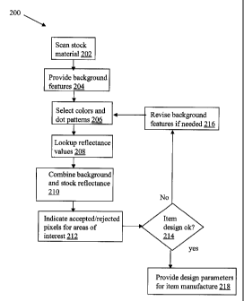
Operation of the System 10
[0061] Referring to Figuresl, 5 and 6, shown is a process 200 for operating
the design system
10 for use in producing the design parameters 14 of the item 12 that is
determined as satisfying
TOR_LAW\ 6985922\1 -21-
CA 02642309 2008-10-29
the reflectance threshold(s) 20 for the selected stock material 16 and the one
or more background
features 18 positioned on the stock material 16.
[0062] Referring to Figure 6, step 202 of the design process 200 provides
(e.g. via the image
capturing device 25) one or more reflectance values Rm of the stock material
16 that is used as a
substrate for placement of the background features 18 and any critical data
thereon. At step 204,
the design parameters 14 of the background features 18 are provided, including
the position,
color and the printing pattein (e.g. dot pattern) 206 of the background
feature(s) 18. At step 208,
the reflectance engine 30 determines the reflectance values Rb for each
portion 21 of the surface
13 of the design image 19 that represents the one or more background
feature(s) 18. At step 210,
the reflectance engine 30 combines the determined background reflectance
values Rb and the
stock material reflectance values Rm to produce the resultant item design
reflectance values Rd.
At step 212, the reflectance values Rd are compared with the appropriate
reflectance threshold(s)
(e.g. for each of the background features 18 present in the areas of interest
AOI of the item 12)
to determine those portions 21 of the item design 42 that either satisfy or do
not satisfy the
15 reflectance threshold(s) 20. At step 214, in the event that certain
portions 21 of the item design
42 have unsatisfactory reflectance values Rd, the design parameters 14 are
revised, including the
selection 206 of the color(s) characteristics and/or color/print density, and
steps 208, 210, 212 are
repeated. At step 214, if the item design 42 is considered acceptable (e.g.
does not contain a
specified number of portions 21 that have reflectance values Rd that do not
satisfy the reflectance
20 threshold(s) 20), the list of corresponding design parameters 14 are
provided to the designer.
Example of Reflectance Engine 30
[0063] Referring to Figure 8, a computing device 101 of the reflectance engine
30 can have a
user interface 102, coupled to a device infrastructure 104 by connection 122,
to interact with a
item designer (not shown). The user interface 102 can include one or more user
input devices
such as but not limited to a QWERTY keyboard, a keypad, a stylus, a mouse, a
microphone and
the user output device such as an LCD screen display and/or a speaker. If the
screen is touch
TOR_LAW\ 6985922\1 -22-
CA 02642309 2008-10-29
4 sensitive, then the display can also be used as the user input device as
controlled by the device
infrastructure 104.
[0064] Referring again to Figure 8, operation of the device 101 is facilitated
by the device
infrastructure 104. The device infrastructure 104 includes one or more
computer processors 108
and can include an associated memory 112 (e.g. a random access memory). The
computer
processor 108 facilitates performance of the device 101 configured for the
intended task (e.g. of
the respective module(s) of the reflectance engine 30) through operation of
the user interface 102
and other application programs/hardware 107 (e.g. modules 32, 34, 38) of the
device 101 by
executing task related instructions. These task related instructions can be
provided by an
operating system, and/or software applications 107 located in the memory 112,
and/or by
operability that is configured into the electronic/digital circuitry of the
processor(s) 108 designed
to perform the specific task(s). Further, it is recognized that the device
infrastructure 104 can
include a computer readable storage medium 110 coupled to the processor 108
for providing
instructions to the processor 108 and/or to load/update the instructions 107.
The computer
readable medium 110 can include hardware and/or software such as, by way of
example only,
magnetic disks, magnetic tape, optically readable medium such as CD/DVD ROMS,
and memory
cards. In each case, the computer readable medium 110 may take the form of a
small disk,
floppy diskette, cassette, hard disk drive, solid-state memory card, or RAM
provided in the
memory module 112. It should be noted that the above listed example computer
readable
mediums 110 can be used either alone or in combination.
[0065] Further, it is recognized that the computing device 101 can include the
executable
applications 107 comprising code or machine readable instructions for
implementing
predetermined functions/operations including those of an operating system and
the reflectance
engine 30 modules, for example. The processor 108 as used herein is a
configured device and/or
set of machine-readable instructions for performing operations as described by
example above.
As used herein, the processor 108 may comprise any one or combination of,
hardware, firmware,
and/or software. The processor 108 acts upon information by manipulating,
analyzing,
modifying, converting or transmitting information for use by an executable
procedure or an
information device, and/or by routing the information with respect to an
output device. The
TOR_LAW\ 6985922\1 - 23 _
CA 02642309 2008-10-29
processor 108 may use or comprise the capabilities of a controller or
microprocessor, for
example. Accordingly, any of the functionality of the reflectance engine 30
(e.g. modules) may
be implemented in hardware, software or a combination of both. Accordingly,
the use of a
processor 108 as a device and/or as a set of machine-readable instructions is
hereafter referred to
generically as a processor/module for sake of simplicity. Further, it is
recognised that the
reflectance engine 30 can include one or more of the computing devices 101
(comprising
hardware and/or software) for implementing the modules, as desired. Further,
it is recognised
that the functionality of the modules 32,34,38 and the lookup table 36 can be
as described above,
can be combined and/or can be further subdivided, as desired. It is also
recognised that the
reflectance values Rm of the stock material can be supplied by the image
capture device 25 to the
input module 32 and/or can be calculated by the input module 32 from
appropriate data included
in the reference image 26 provided by the image capture device 25 to the input
module 32, as
desired.
TOR_LAW\ 6985922\1 - 24 -