Note: Descriptions are shown in the official language in which they were submitted.
CA 02642426 2012-08-13
FIBER-TO-THE-HOME (MR) OPTICAL RECEIVER
WITH DISTRIBUTED GAIN CONTROL
FIELD OF THE INVENTION
The present invention relates to fiber-to-the-home (FTTH) optical transmission
systems
and more particularly to an FTTH optical receiver used in such system having
distributed gain
control for receiving and processing video, voice, and data optical signals
while maintaining
optimum performance.
BACKGROUND OF THE INVENTION
In recent years there has been a great deal of interest in the transmission of
video, voice,
and data signals via optical fiber that is pulled to the home, i.e., fiber-to-
the-home (FTTH)
systems. Traditionally, cable operators have provided video and data signals
over a hybrid
fiber/coaxial cable (HFC) system. In an FTTH system, optical signals are sent
via optical fiber
for transmission over longer distances. The optical signals are then converted
to radio frequency
(RF) signals for transmission over coaxial cable just before entering the
home. In contrast,
telephone operators have traditionally provided voice and data signals via
optical fiber that is
pulled to the home, and the signals then enter the home via twisted pair cable
as opposed to
coaxial cable. As the demand for video, voice, and data services continues to
grow, optical fiber
solutions continue to gain momentum over the traditional HFC and telephony
systems for both the
cable and telephone operators. In addition, there are several advantages for
utilizing optical fiber
that is pulled closer to the home for providing cable and telephone services.
Advantageously, optical fiber systems typically enjoy a high signal quality;
lower
maintenance and easier troubleshooting; a low attenuation rate; and easy
system expansion, to
1
CA 02642426 2008-08-14
WO 2007/100983
PCT/US2007/062167
name but a few. Conversely, some of the disadvantages with an optical fiber
system are
maintaining gain control, powering and power consumption, installation, and
simplicity
requirements with the equipment, such as optical receivers. What is needed,
therefore, is an
optical receiver that is capable of offering a complete package of broadband
services including
video, voice, and data signals over a fiber-to-the-home (FTTH) system while
overcoming any of
the disadvantages.
2
CA 02642426 2008-08-14
WO 2007/100983
PCT/US2007/062167
BRIEF DESCRIPTION OF THE DRAWINGS
FIG. 1 illustrates a block diagram of a conventional fiber-to-the-home (FTTH)
optical
receiver.
FIG. 2 illustrates a detailed diagram of a triplexer that is suitable for use
in the FTTH
optical receiver of FIG. 1.
FIG. 3 is a first embodiment of an optical receiver in accordance with the
present that is
suitable for use in an FTTH system.
FIG. 4 is a second embodiment of an optical receiver in accordance with the
present
invention that is suitable for use in an FTTH system.
3
CA 02642426 2008-08-14
WO 2007/100983 PCT/US2007/062167
DETAILED DESCRIPTION OF A PREFERRED EMBODIMENT
The present invention will be described more fully hereinafter with reference
to the
accompanying drawings in which like numerals represent like elements
throughout the several
figures, and in which exemplary embodiments of the invention are shown. This
invention may,
however, be embodied in many different forms and should not be construed as
limited to the
embodiments set forth herein; rather, the embodiments are provided so that
this disclosure will be
thorough and complete, and will fully convey the scope of the invention to
those skilled in the art.
For example, the present invention may be embodied using discrete components
and MMIC
amplifiers. Additionally, the present invention may be embodied using a custom
RFIC that is
incorporated into one integrated circuit. Furthermore, the present invention
may also be
combined with an optical photodiode, either by co-locating the two in one
package or using the
same substrate for both optics and radio frequency (RF) electronics. The
present invention may
be mounted within an enclosure located on an outside wall of a home or
business. As such, the
power dissipation should be minimized and the circuitry designed for the
outdoor environment.
Therefore, thermally compensated automatic gain circuitry is important to
maintain performance
over temperature variations.
It will be appreciated that the present invention addresses the need for an
optical receiver
that is designed for a fiber-to-the-home (FTTH) system. However, the present
invention is not
limited to an FTTH system. More specifically, the present invention can also
be used in a fiber-
to-the-curb (FTTC) system, a fiber-to-the-business (FTTB) system, or a hybrid
fiber/coax (HFC)
system. Advantageously, in accordance with the present invention, the gain
control circuits are
distributed throughout the optical receiver in stages in order to address
noise and distortion
performance, gain control, low power consumption, and a well controlled radio
frequency (RF)
output level. In this manner, the design of the optical receiver allows FTTH
systems the benefit
of an extended optical input range while maintaining the required system
specifications.
FIG. I illustrates a block diagram of a conventional fiber-to-the-home (FTTH)
optical
receiver 100. The FTTH optical receiver 100 is capable of receiving multiple
wavelength optical
signals including video, voice, and data signals from a service provider
located upstream. For
4
CA 02642426 2008-08-14
WO 2007/100983 PCT/US2007/062167
example, video signals may be sent on a 1550 nanometer (nm) wavelength;
downstream, or
forward, voice and data signals may be sent using a 1490 nm wavelength; and
upstream, or
reverse, voice and data signals may be sent using a 1310 nm wavelength. It
will be appreciated
that wavelengths may differ depending on the fiber equipment used throughout
the FTTH system.
The FTTH optical receiver 100 is housed within a home mounted unit, such as an
optical network
unit (ONU) (not shown). The home mounted unit may include additional telephony
circuitry for
processing the voice and data signals. The voice and data signals may then be
provided to the
appropriate home equipment via twisted pair cable in a conventional manner.
In addition to the voice and data signals, the optical receiver 100 receives
and processes
video/audio signals. This is a significant improvement over the conventional
ONU that processes
exclusively voice and data signals. In this manner, a traditional telephone or
cable operator that
may already have an FTTH system in place can add the FTTH optical receiver 100
to an existing
ONU and process video, voice, and data signals. Typically, the video signals
provided to the
home via the FTTH optical receiver 100 are of equal or better quality than the
video signals that
are provided by a conventional HFC system.
A triplexer 105 distinguishes and separates the different signals having
varying
wavelengths. These separated signals are then provided to appropriate devices
within the ONU or
the FTTH optical receiver 100 for further processing. FIG. 2 illustrates a
detailed diagram of the
triplexer 105 that is suitable for use in the FTTH optical receiver 100. The
triplexer 105 receives
the optical signals and, depending upon the wavelength of the received
signals, routes them to an
appropriate internal photodiode. More specifically, a video mirror 205
reflects the video signals
determined by the wavelength to a video photodiode 210. Currently, the
preferable wavelength
for transmitting video signals is at 1550 to 1560 nm due to existing fiber
equipment; low losses in
the fiber at this wavelength; EDFA technology; and the availability of lasers,
to name a few. The
video photodiode 210 provides video signals in a forward frequency to
amplifier stages within the
FTTH optical receiver 100. A typical forward frequency used for video signals
is from 45 to
1000 Mega Hertz (MHz). A second mirror 215 reflects a second wavelength, for
example, 1490
nm, to a second photodiode 220. The second photodiode 220 then outputs a
digital stream at, for
5
CA 02642426 2012-08-13
,
example, 155 mega bits per second (mbps) that includes the voice and data
signals. A laser 225
provides an optical digital stream output at, for example, 155 mbps that
includes the voice and
data signals. The digital photodiode 220 and laser 225 provide the digital
streams to and from
additional circuitry (not shown) in the ONU for processing in a conventional
manner and then to
twisted pair cable that is routed throughout the home. It will be appreciated,
however, that a
diplexer or a standard photodiode can be used for video services only. Further
infomtation
regarding the triplexer that can be used in an optical receiver can be found
in U.S. patent no.
6,674,967 entitled "Fiber To The Home (vrao Optical Receiver having Gain
Control and a
Remote Enable" by a common inventor.
Referring again to FIG. 1, the video photodiode 210 has three outputs. Two
outputs are
provided to a transformer 110 for matching the video signals to a preamplifier
stage; a third
output (not shown) is a ground pin. It will be appreciated that the matching
can be accomplished
in a number of ways, but a preferred embodiment of the present invention
accomplishes the
matching through the transformer 110 and a bias network 112. These also serve
to improve the
optical receiver noise performance. The photodiode 210 and the transformer 110
provide two
anti-phased RF current connections, one at 0 and one at 180 , to the inputs
of two push-pull
amplifiers 115, 120. The broadband current signals from the photodiode 210 are
converted to
amplified RF voltage signals in the amplifiers 115, 120 before being coupled
to a combining
transformer 125.
Gain stages comprising amplifiers 115, 120 and 140, 145 utilize a push-pull
application
as described in U.S. Patent No. 5,347,389. The
gain stages (i.e., preamplifier stage and postamplifier stage) are designed to
provide sufficient
gain to drive a home network that has typical losses associated with a 4-way
splitter and coaxial
cable. It will be appreciated that the amplifiers 115, 120, 140, 145 could,
alternatively, be single
ended amplifier stages, as long as their linearity performance is sufficient.
Using single ended
amplifiers also eliminates transformers 125 and 135, thereby reducing costs.
6
CA 02642426 2008-08-14
WO 2007/100983 PCT/US2007/062167
A gain control and tilt combination network 130 receives the combined RF
signal. The
gain control portion of the network 130 compensates for a wide range of input
optical power
provided by the FTTH system. It will be appreciated that it is possible to
construct an FTTH
system without requiring a gain control network. In this manner, however, the
operator must
construct a system with predetermined optical fiber lengths and known RF input
levels of the
home in order to set the amplifier stages to the appropriate level. Though
more difficult to design
and implement, it will also be appreciated that if a gain control network is
not used, transformers
125, 135 are no longer necessary. In the preferred embodiment of the present
invention, however,
the gain control portion of the network 130 is provided to accommodate
flexibility in systems
having varying fiber lengths and RF input levels.
The gain control network 130 is an open loop gain control network that derives
the
appropriate gain by sensing the optical input power level from the output of
the photodiode 210.
A predetermined backoff amount is set to maintain an acceptable input signal
level to the home.
A bridge-tee circuit utilizing PIN diodes, for example, sets the predetermined
backoff in the
network 130. In this manner, installation of the FTTH optical receiver 100 is
simplified by using
the predetermined backoff because there is no need to set the output RF level
as required by
conventional optical receivers and amplifiers. Additionally, the predetermined
backoff amount is
valid if the Optical Modulation Index (OMI) is known and constant. A less
expensive AGC
network approach involves limiting the gain variability to either a 0 dB loss
or a 10 dB loss. The
threshold point can be adjusted to optimize noise performance, but keep the RF
output levels
within allowable limits. A hysteresis network can also be implemented to
control the circuitry
and eliminate any oscillatory states around the threshold point.
The gain control portion of the network 130 is an interstage device located
between the
preamplifier stage and a postamplifier stage. Alternatively, the gain control
could be placed at the
output of the receiver 100; however, interstage positioning reduces the
linearity requirements of
the postamplifier. The output of the gain control and tilt network 130 is
provided to a transformer
135 for matching the RF signal to two push-pull postamplifiers 140 and 145. A
final transformer
7
CA 02642426 2008-08-14
WO 2007/100983 PCT/US2007/062167
150 receives the amplified RF signals and combines the RF signals for
transmission through the
coaxial cable to, for example, a set-top device.
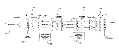
FIG. 3 is a first embodiment of an optical receiver in accordance with the
present
invention that is suitable for use in an FTTH system. The optical receiver 300
in accordance with
the present invention utilizes several gain stages as opposed to the
conventional optical receiver
100 of FIG. 1. More specifically, in accordance with the present invention,
the gain stages 320,
335, 350, 360 are distributed throughout the optical receiver 300 rather than
just implementing a
preamplifier and a postamplifier stage as shown in FIG. 1. In a conventional
optical receiver 100,
a higher power gain stage is required to maintain the linearity specifications
of the RF output that
is required due to the fluctuating input optical level in an FTTH system.
Conversely, in
accordance with the present invention noise performance is optimized and RF
signal levels are
prevented from increasing beyond the gain stages linear region, thus allowing
for smaller, lower
power consumption gain stages. It will be appreciated that the stages can be
implemented in
different ways, such as using an open or a closed loop circuit, a
predetermined backoff or RF
filters and detectors if the OMI is not known or may change due to channel
loading.
A photodiode 305 receives the input optical signal and converts the optical
signal into an
RF signal. It will be appreciated that the photodiode 305 can be a stand-alone
device if external
wave division multiplexing (WDM) components are used. Additionally, the
photodiode 305 as
shown could also be a diplexer or a triplexer module that includes the WDM
components.
Furthermore, the photodiode 305 can be biased in a number of ways such as
integrated together
with a receiver integrated circuit, but in a preferred embodiment of the
present invention it is
accomplished through a bias network 308 and a transformer 310, which also
serves to improve
optical receiver noise performance.
The RF output of the photodiode 305 is provided to preamplifier stage 320. The
preamplifier stage 320, including transformers 310, 315 and amplifiers,
matches the RF output
signal to a lower output impedance. It will be appreciated that the stages
320, 335, 350, 360 are
designed to provide sufficient gain to drive a home network comprising a 4-way
splitter and
coaxial cable loss. The final RF output impedance of the optical receiver 300
is 75 Ohms, which
8
CA 02642426 2008-08-14
WO 2007/100983 PCT/US2007/062167
is a typical requirement for an in-home distribution network. It will also be
appreciated that in a
preferred embodiment of the present invention, the amplifiers in the stages
are push-pull circuits,
but could be single ended stages, if linearity performance is sufficient. As
mentioned, a single-
ended stage or push pull circuits used concurrently 350 and 360, would
eliminate some
transformers in the optical receiver, thereby reducing cost. If the input
noise performance of the
preamplifier stage 320 is low, cost may also be reduced by eliminating the
input transformer 310
and biasing the photodiode 305 through RF inductor chokes in a known manner.
Attenuator 325 and gain control network 330 compensate for a wide input
optical power
that could be received from the FTTH system. Prior to any gain control, a
possible 15 dB
variation in input optical power correlates to a 30 dB variation in RF level,
which is excessive for
connected televisions and set-top terminals in the home network. Accordingly,
attenuators and
gain control circuits are necessary to maintain an acceptable input signal
level to the home, while
maintaining the requirements for good noise performance, good linearity, and
low power
consumption. A preferred embodiment of the present invention incorporates an
open loop
compensation circuit derived from a sense line from the photodiode 305.
Optical input power is
first sensed by optical detection circuitry included in the gain control
circuit 330. A first
attenuator 325 then attenuates the input signal level when the optical level
increases in power
beyond a predetermined threshold. This allows the optical receiver 300 to
optimize its noise
performance until the system that provides the input optical signal achieves a
sufficient signal-to-
noise level. As the input signal level attenuates, the noise of the optical
receiver 300 is degraded;
however, this attenuation helps achieve the desirable output linearity
requirement by preventing
the input signal from over-driving the interstage amplifier 335 and each
subsequent gain stage
350, 360.
A second attenuator 340 is always operational and located after the first two
gain stages
320, 335. With the location between the two stages 335, 350, the second
attenuator 340 limits its
direct effect on the noise performance of the optical receiver. More
specifically, the second
attenuator 340 allows the first attenuator 325 the capability of delaying when
it switches to allow
better noise performance. When the first attenuator 325 switches, the second
attenuator 340 backs
9
CA 02642426 2012-08-13
off automatically to maintain a desired level. Additionally, since the
attenuator 340 is located
prior to the output gain stages 350, 360, the RF level of the signal is
further attenuated prior to
output gain stages 350, 360. This additional attenuation allows the optical
receiver 300 to have a
constant output level and prevents the output gain stages 350, 360 from being
overdriven into a
non-linear region. The closed-loop second attenuator 340 uses a power
detection circuit and
receives its input from coupler 370. Additionally, coupler 370 provides the RF
output signal to
the home network.
As also shown in FIG 3, the optical receiver 300 of the present invention can
also include
remote enabling. The service provider can disable the optical receiver 300
remotely through the
network. The communication between the service provider and the optical
receiver 300 uses a
wavelength on the fiber to provide a bidirectional digital signal path. The
enable function
interrupts power to the gain stages 320, 335, 350, 360, thereby providing
adequate isolation to
shut off any video signals to the home. The bias for the photodiode 305 is
still maintained,
however, which allows monitoring of the optical signal integrity, regardless
of the state of the
video output. An additional benefit is the reduction in power consumption of
the home mounted
unit, if video service is not desired.
FIG. 4 is a second embodiment of an optical receiver in accordance with the
present
invention. An integrated circuit 405 incorporates a preamplifier stage 415 and
a first interstage
amplifier 430 into one package. It will be appreciated that the integrated
circuit 405 can also be
coupled to the photodiode 305 either by co-locating the two circuits in one
package or using the
same substrate for both optics and RF electronics. The optical receiver 400
can then be mounted
within an enclosure on an outside wall of a home or business. Included in the
integrated circuit
405 may also be a bias network 410 and remote enabling. Gain control circuits
420, 425 are
coupled between the preamplifier stage 415 and the interstage amplifier 430.
The optical receiver 400 also comprises an attenuator 340 and RF detection and
automatic
gain control circuitry 345. A tilt network 435 is then coupled between the
second interstage
amplifier 350 and the postamplifier stage 360 to ensure that the RF output is
provided with the
appropriate tilt for the in-home network due to any RF cable losses. Also
included is a coupler
CA 02642426 2012-08-13
440 that operates as an RF test point allowing the service provider to verify
the RF levels at the
output of the receiver 400.
The above describes an optical receiver in accordance with the present
invention that
addresses the need to receive a varying wide input optical signal and continue
to provide a linear
RF output with good noise distortion performance. It will also be appreciated
that as mentioned
there are several different embodiments of the optical receiver that perform
in a like manner as the
embodiments shown. The scope of the claims should not be limited by the
preferrered
embodiments and the examples but should be given the broadest interpretation
consistent with the description as a whole.
11