Note: Descriptions are shown in the official language in which they were submitted.
CA 02642527 2008-08-07
WO 2007/092955 PCT/US2007/061928
SCALABLE INTELLIGENT POWER SUPPLY SYSTEM AND METHOD
This patent application claims priority of United States provisional
application serial number 60/771,771 filed February 9, 2006 and United States
provisional application serial number 60/781,959 filed March 12, 2006.
Priority is
also claimed to United States patent application serial no. 11672853 filed
February
8, 2007 and United States patent application serial no. 11672957 Filed
February 8,
2007. All of the aforementioned applications are in the name of the inventor,
Karl
F. Scheucher.
FIELD OF THE INVENTION
The field of invention is in the field of intelligent power supply systems
having multiple alternating and direct current inputs and outputs and
rechargeable,
interchangeable backup energy sources. Additionally, the invention is in the
field
of interchangeable battery powered electric vehicle management systems which
include rechargeable, swap-able and replaceable battery packs at electric
vehicle
refueling stations.
BACKGROUND OF THE INVENTION
United States Patent No. 6,465,986 B 1 issued October 15, 2002 discloses
battery interconnection networks electrically connected to one another to
provide a
three-dimensional network of batteries. Each of the interconnection networks
i
CA 02642527 2008-08-07
WO 2007/092955 PCT/US2007/061928
comprises a battery interconnection network having a plurality of individual
component batteries configured with compound series parallel connections. A
plurality of rows of individual component batteries are connected in parallel.
A
plurality of columns of individual component batteries are interconnected with
the
plurality of rows with each column having a plurality of individual component
batteries connected in series with an adjacent individual component battery in
the
same column and electrically connected in parallel with an adjacent individual
component battery in the same row.
McDowell Research Corporation of Waco, Texas produces a Briefcase
Power System for powering transceivers with an advertised DC input range of 11
to 36 VDC and an AC input range of 95 to 270VAC at 47 to 440 Hz. No outputs
are specified in the advertisement at www.mcdowellresearch.com.
Automated Business Power, Inc. of Gaithersburg, Maryland produces an
Uninterruptible Power Supply Transceiver Power Unit with advertised DC input
range of 9 to 36VDC and AC input range of 85 to 270VAC at 47 to 440 Hz. Two
outputs are specified both at 26.5VDC, one at 5.25 A and one called auxiliary
at
1A. Battery chemistry is not specified in the advertisement at www.abpco.com,
but indications are given that non-compatible battery types including primary
Lithium battery (BA-5590/U), NiCd (BB-590/U), NiMH (BB-390A/U) or any
2
CA 02642527 2008-08-07
WO 2007/092955 PCT/US2007/061928
other non-compatible type shall not be useable.
There is a need for a light-weight intelligent energy system for use in a
variety of applications including for use in energy supply systems for
homeland
defense, military, industrial and residential use. There is also a need for
light-
weight energy systems including battery systems for use in vehicles, cars,
trucks,
military vehicles and the like which can be refueled by swapping individual
batteries or groups of batteries at energy filling stations much like the
typical gas
stations.
SUMMARY OF THE INVENTION
The circuitry and control methodology described herein is applicable to use
of modular energy supply systems in automobiles. For instance, the control
methodology described herein may be used in connection with Lithium ion
batteries used in an automobile. In this way, the batteries may be removed
from
the automobile and recharged at a service station and then replaced into the
vehicle
fully charged. The batteries may be separately removed from the automobile or
they may be removed in groups. The invention as taught and described herein
enables the evaluation of individual batteries and the evaluation of the
energy
remaining in the batteries at the time they are swapped out (exchanged) for
fully
charged batteries. In this way a motorist can effectively refuel his or her
vehicle
3
CA 02642527 2008-08-07
WO 2007/092955 PCT/US2007/061928
and proceed on his or her way without worrying about stopping to charge the
batteries which is time consuming as the recharge time for Lithium ion
batteries is
considerable. Having the ability to quickly swap the batteries in a Lithium
ion car
enables the driver to get credit for the energy in his "gas" tank. In reality
the
teachings of the instant invention enable the driver to effectively have an
"energy
tank" as compared to a "gas tank."
A power supply is disclosed which includes multiple alternating current and
direct current inputs and outputs. One of the inputs is a back-up energy
source
which is carried on board within the power supply. The back-up energy source
may be batteries or fuel cells. An enclosure used to house the power supply is
expandable to include additional battery racks each housed within an
individual
frame of the enclosure. A power supply may also be expanded by interconnecting
separate enclosures with the use of appropriate cables.
The power supply is microprocessor controlled based on the status (voltage,
current and temperature) of the inputs including the status of the back-up
energy
source, the status of converters and internal buses, and the status of the
outputs.
The microprocessor manages the back-up energy source and the overall operation
of the power supply by selectively coupling system inputs, buses and outputs.
Where power sources are combined in an "or" relationship, diodes or their
4
CA 02642527 2008-08-07
WO 2007/092955 PCT/US2007/061928
equivalents are used to prohibit undesirable current flows. MOSFET based
switches or their equivalents controlled by the microprocessor are used
extensively
in the selective coupling of the system inputs, buses and outputs.
The power supply disclosed herein resides in one or more weatherproof
enclosures housing a battery rack having a plurality of batteries in at least
one
frame portion. First and second fastening bars are affixed to the frame
portion.
First and second connecting rods are attached to the first and second
fastening bars
and extend therefrom; the battery rack includes a frame fastener and first and
second fastening bars interconnect with the frame fastener to secure the
battery
rack to the frame. A rearward portion of the frame includes an electrical
motherboard mounted thereon. A front door portion of the frame may include one
or more vents and fans.
Alternatively, the power supply is mounted in an enclosure which includes a
plurality of frame portions connected to one another via robust hinges and
latches
with weatherproof gasketing along the entire frame to frame interface
surfaces. A
plurality of battery racks reside within the power supply with one rack
residing in
each frame and being secured thereto. Since the frames are hinged together
they
may be separated from each other for maintenance. Additional frames may be
added to allow greater power levels or extended operating time or both.
Likewise
CA 02642527 2008-08-07
WO 2007/092955 PCT/US2007/061928
one or more frames may be removed if the power level or operating time they
represent becomes superfluous. Each rack includes a plurality of batteries in
electrical communication with a motherboard which resides in the rearward-most
portion of the plurality of frame portions hinged together. The front-most
frame is
a front door portion which includes vents and fans to cool the batteries and
electronics of the power supply. Other relative positions of frame modules are
possible and anticipated. For instance, vents and fans may be positioned in
the
rearward-most frame. The front-most frame may contain the motherboard.
Alternatively, an intermediate frame may contain the motherboard and rearward-
most and front-most frames could both contain fans and/or vents.
A process for servicing the embodiment of the power supply which includes
a plurality of frame portions hinged together (with each frame securing an
arrayed
rack of batteries) includes the steps of: unlocking the latch side of a frame
from the
next adjacent frame; and, rotating the next adjacent frame about its hinged
side to
expose the frame to be serviced. The next adjacent frame may be the rearward-
most frame which includes the motherboard for controlling each rack containing
a
plurality of arrayed batteries. The next adjacent frame may be any frame
intermediate the rearward-most frame and the front-most frame. Each frame may
be separated from the next adjacent frame as the frames are hinged together.
Removal of the hinge pin from the hinge may accomplish the separation of the
6
CA 02642527 2008-08-07
WO 2007/092955 PCT/US2007/061928
frames, or removal of fasteners retaining flanges associated with the hinges
to a
frame may perform the separation, or other logical means of disconnecting
framed,
door-like, hinge connected modules from one another may be employed.
Alternatively, the above described frame portions may be separately
enclosed and interconnected as required using appropriate weatherproof cable
assemblies. A rack for housing a plurality of removable cartridge batteries
includes
a plurality of shelves arranged in a stack type relationship. The stack
includes a
bottom shelf and a top shelf. Intermediate shelves residing between the bottom
shelf and the top shelf are vertically spaced apart from each other. The
shelves
include a plurality of bores therethrough with interconnecting rods extending
vertically through the bores in the shelves. A plurality of hollow spacing
tubes
(spacers) reside concentrically around the plurality of interconnecting rods
and
intermediate each of the shelves spacing them apart. Fasteners, such as nuts,
are
affixed to the interconnecting rods beneath the bottom shelf and above the top
shelf. Other techniques of construction are also contemplated wherein the
spatial
relationship of the shelves and overall ruggedness of the structure is
maintained
comparable to the above described connecting rod and spacing tube construction
technique. These other techniques may include formed sheet metal components
welded together or connected by fasteners to form a superstructure into which
the
shelf elements may be placed and securely retained by features of the
engagement
7
CA 02642527 2008-08-07
WO 2007/092955 PCT/US2007/061928
between the sheet metal and shelf elements (snap together construction) or by
additional fasteners or other adhesive techniques.
Each of the removable cartridge type batteries includes a first electrical
contact and a second electrical contact. The removable cartridge type
batteries
may be removable cordless tool batteries. Each shelf contains one or more
battery
docking locations. Each docking location includes a first electrical connector
which matingly engages the first electrical contact of the battery and a
second
electrical connector which matingly engages the second electrical contact.
First and
second wires are affixed to the first and second electrical connectors and are
routed
to a battery interface circuit. Additional contacts and corresponding
electrical
contacts may be present upon batteries and docking locations.
Alternatively, the shelves may include battery interface circuits in the form
of printed circuits thereon. Each shelf includes a connector for communication
with
another board, typically a rack common board which in turn connects typically
to
the aforementioned motherboard. In this example the first and second
connectors
engage and are electrically connected to appropriate points of each respective
printed circuit.
The power supply includes a programmable microprocessor for managing
inputs, internal components and outputs based on continuously sampled and
processed voltage, current and temperature measurements. An alternating
current
8
CA 02642527 2008-08-07
WO 2007/092955 PCT/US2007/061928
input source is selectively coupled to an AC/DC converter which, in turn, is
selectively coupled with an intermediate DC bus and/or a second DC bus and/or
a
third DC bus. First, second, and third direct current input sources are
selectively
coupled with the intermediate DC bus and/or the first DC bus and/or the second
DC bus and/or the third DC bus. The intermediate DC bus is selectively coupled
with a first DC output and/or a DC/AC inverter and/or a third DC/DC converter.
The third DC/DC converter is coupled to a second DC output and a third DC
output. The first DC bus is coupled to a first DC/DC converter which, in turn,
is
selectively coupled to the intermediate DC bus and/or the third DC bus and/or
a
DC charge bus.
The second DC bus is coupled to a second DC/DC converter which, in turn,
is selectively coupled to the intermediate DC bus and/or the third DC bus
and/or
the DC charge bus.
The third DC bus is coupled to a fourth DC output and the third DC bus is
selectively coupled to a fourth DC/DC converter which, in turn, is coupled to
a
fifth and sixth direct current output. The charge bus is coupled to the third
direct
current input source. The third direct current input source is the battery
back-up
current source containing literally almost any number of individual batteries.
Batteries over a wide range of inputs from 10 to 40 VDC will be used. However,
it
is specifically envisioned that batteries over a wider range such as 1.5 VDC
up to
9
CA 02642527 2008-08-07
WO 2007/092955 PCT/US2007/061928
hundreds of volts direct current may be used provided appropriate circuit
element
adaptations are made such as utilizing switches rated for the voltage ranges
being
switched.
As previously stated, the power supply includes a microprocessor and the
third direct current input source includes a nearly limitless plurality of
removable
cartridge battery packs. Each of the removable cartridge battery packs is
selectively
connected or disconnected with a battery bus interconnected with a load. Each
of
the removable cartridge battery packs is also selectively connected or
disconnected
with a charge bus.
One exemplary algorithm for operation of the plurality of batteries is as
follows. The microprocessor selectively connects a first portion of the
plurality of
removable cartridge battery packs with the battery bus. The microprocessor
selectively connects a second portion of the plurality of removable cartridge
battery packs with the charge bus. The microprocessor selectively connects a
third
portion of the plurality of removable cartridge battery packs with both the
battery
bus and the charge bus. The microprocessor selectively disconnects a,fourth
portion of the plurality of removable cartridge packs from both the charge bus
and
the battery bus.
The first, second, third and fourth portions of the plurality of removable
cartridge battery packs may include one, more than one, all, or none of the
plurality
CA 02642527 2008-08-07
WO 2007/092955 PCT/US2007/061928
of removable cartridge battery packs. The plurality of removable cartridge
battery
packs may include batteries having different nominal voltages. "Nominal
voltage"
as used herein means the voltage across a fully charged battery, namely, the
open
circuit voltage.
One exemplary process for operating a power supply having a plurality of
battery packs is disclosed and includes the steps of: monitoring the battery
bus
output branch associated with each of the selected battery packs and measuring
the
voltages thereon while supplying a load which includes a direct current to
direct
current step up converter; monitoring the battery bus output branch associated
with
each of the selected battery packs and measuring the voltages thereon while
disconnected from the load; comparing the unloaded and loaded voltages of each
respective battery selected for operation and connection to the load; and,
identifying battery packs to be charged depending on the comparison of the
unloaded and loaded voltages on each of the respective battery bus output
branch(es). The process can also include the step of charging the identified
battery
packs. Still additionally, the process can include the step of charging the
identified
battery packs at a voltage higher than the nominal voltage of each of the
battery
packs.
The battery back-up direct current input can be virtually limitless in size.
Multiple frames can house multiple racks of back-up batteries. The back-up
ii
CA 02642527 2008-08-07
WO 2007/092955 PCT/US2007/061928
batteries are expected to be in the range of 10 VDC to 40 VDC. Commercially
available cordless tool batteries are in this range. Therefore, the power
supply
disclosed and claimed herein includes a microprocessor and up to K batteries
in
parallel, where K is any positive integer. I disclose battery arrays having 20
Li-Ion
batteries per rack. In the 20 battery per rack example each battery has a
nominal
unloaded voltage of 18 VDC. Each battery has a battery interface circuit which
switchably interconnects each battery with up to N loads where N is any
positive
integer. Each battery is switchably connected (through the battery interface
circuit)
with the charge bus. The back-up batteries are connected in parallel and may
be
removed for use in another application such as in another power supply or in a
cordless tool, other cordless appliance, vehicle, or other backup energy
application.
A monitor bus is also switchably interconnected by the battery interface
circuit of
each battery and may monitor up to K batteries. Lastly, a sense resistor bus
switchably interconnects with up to K batteries. The microprocessor directs
power
into and out of each described bus controlling up to K battery connections
with up
to N load, charge, monitor, and sense buses.
The microprocessor also prioritizes up to N loads and disconnects the loads
in a prescribed order as to their relative importance at prescribed levels or
remaining energy as remaining backup energy diminishes through periods of
continuing operation.
12
CA 02642527 2008-08-07
WO 2007/092955 PCT/US2007/061928
Another embodiment of the power supply includes a plurality of hot-
swappable removable cartridge battery packs in parallel interconnected with
either
a DC-AC inverter or with a DC-DC converter which in turn leads to the DC-AC
inverter after the DC voltage is appropriately modified. Usually this
modification
will involve a step-up of the voltage. The DC-AC inverter provides an AC
output.
The removable cartridge battery packs are arranged in parallel with each other
and
include a common battery bus for communicating power to the DC-AC inverter.
Each of the battery packs includes an output and a diode or equivalent circuit
substituting the diode function arranged in series with the output of the
battery
pack communicating power to the common battery bus. It should be noted that
alternative circuit implementations are possible and contemplated.
The AC-DC input is fed to an AC-DC converter and then is ored together
with the output of the DC-DC converter. Alternatively, the output of the AC-DC
converter could be ored together with the common battery bus if no
modification
of the common battery bus DC voltage is desired.
The output of the AC-DC converter is interconnected in series with a diode
and said common battery bus is interconnected in series with a diode and the
diodes are interconnected in an oring fashion. In this fashion the diodes or
equivalent circuits protect the common battery bus and/or the DC-DC converter
and/or the AC-DC converter from back fed current. The diodes are commonly
13
CA 02642527 2008-08-07
WO 2007/092955 PCT/US2007/061928
joined in a bus which is interconnected with the DC-AC inverter.
The conceptual management hierarchy of the power supply system is
disclosed herein. Using this hierarchical arrangement the network management
user may access the status and control parameters for all subsystems under a
particular gateway. Information is shown for the batteries (energy subsystems
and
energy modules), inputs, converters, and outputs (power conversion and control
units), and gateway. All aspects of the underlying power supply status and
operation may be monitored and controlled by the user via this network. Up to
P
power conversion and control units may be (where P is a positive integer)
connected for management purposes to each gateway. Similarly, up to S energy
subsystems (where S is a positive integer) may be connected for management
purposes to each power conversion and control unit. Up to M energy modules
(where M is a positive integer) may be connected for management purposes to
each energy subsystem. Energy modules include but are not limited to lithium
ion
based batteries.
By virtue of this hierarchical arrangement the power supply user may
configure and control a power supply systems under a particular gateway. For
example, one such physical arrangement may be a gateway unit connected to at
least one power conversion and control unit which in turn is connected to at
least
one energy subsystem which in turn is connected to at least one energy module.
14
CA 02642527 2008-08-07
WO 2007/092955 PCT/US2007/061928
As long as at least one energy subsystem having at least one energy module is
connected to a power conversion and control unit, the power conversion and
control unit may continue to operate provide power and management control to
the
user.
It is an object of the invention to provide a power supply wherein at least
one input is a back-up energy source and wherein the back-up energy source is
rechargeable within the battery rack, is rechargeable within the rack but with
the
rack removed from the power supply, or is rechargeable when removed from the
rack and from the power supply.
It is an object of the invention to provide a power supply wherein a back-up
energy source includes a rack of individually controlled and rechargeable
removable cartridge type energy packs.
It is an object of the invention to provide a power supply wherein removable
cartridge type energy packs are batteries.
It is an object of the invention to provide a power supply wherein removable
cartridge type energy packs are batteries at different voltages.
It is an object of the invention to provide a power supply capable of
receiving I (where I is a positive integer) AC or DC inputs and controlling,
measuring, sensing, charging and converting those inputs.
It is an object of the invention to provide a power supply capable of
CA 02642527 2008-08-07
WO 2007/092955 PCT/US2007/061928
supplying Q (where Q is a positive integer) AC or DC outputs and controlling,
measuring, and sensing, those outputs.
It is an object of the invention to provide a power supply capable of
managing I AC or DC inputs and managing Q AC or DC outputs by periodically
and continuously sampling and measuring system currents, voltages and
temperatures.
It is an object of the invention to provide a power supply having I AC or DC
inputs wherein at least one of those inputs is back-up energy source which may
be
a fuel cell rack, an atomic-powered generator rack, a Li-lon battery rack, a
NiMH
battery rack, a NiCd battery rack, a lead acid battery rack, a Li-lon polymer
battery
rack, or an Alkaline battery rack. It is an object to provide a microprocessor
controlled intelligent power supply which effectively manages its backup power
supply input.
It is an object of the present invention to provide a power supply having a
DC input from a plurality of removable, hot-swappable, and interchangeable
batteries which provide power on a common battery bus to a DC-AC inverter.
Alternatively, and additionally, AC power may be supplied to the power supply
through an AC-DC converter which is then converted back to AC for purposes of
reliability and for the purpose of seamless transition (uninterruptible power
supply
on-line topology). The output of the DC to AC converter is arranged in a diode
16
CA 02642527 2008-08-07
WO 2007/092955 PCT/US2007/061928
oring fashion together with the output from the common battery bus. The diode
oring selects the higher voltage in converting from DC to AC power. Further,
the
common battery bus voltage may be converted by a DC to DC converter
intermediate the common battery bus and the diode in series leading to the
junction
with the output of the AC-DC converter. Use of the DC to DC converter enables
use of rechargeable batteries which have a relatively low output voltage. It
is an
object of the invention, in this example, to provide a power supply which does
not
require a microprocessor to manage its operations. Rather, this example
provides a
seamless transition from an AC power input to a DC power input with hot-
swappablility of the batteries. The batteries may be cordless tool batteries
capable
of dual use. Further, the batteries may be Li-Ion or any of the types referred
to
herein.
It is an object of the invention to enable use of batteries in an electric or
hybrid automobile such that the batteries may be interchanged and exchanged at
a
service station.
It is an object of the invention to enable the use of electric vehicles by
intelligently interchanging the batteries of the vehicles at a service
station.
It is an object of the invention to enable the use of electric batteries in a
vehicle such as a car wherein the electric batteries are interchanged at a
service
station and credit is given for the energy left in the batteries.
17
CA 02642527 2008-08-07
WO 2007/092955 PCT/US2007/061928
It is an object of the invention to enable use of electric vehicles anywhere
over long distances at high speeds without lengthy recharge periods as the
batteries
may be replaced at service stations just as a gasoline powered car is fueled
at a
gasoline service station.
It is an object of the invention to enable electric vehicles having batteries
arranged in series or parallel to be interchanged at a service station.
It is an object of the invention to enable continuous operation of electric
vehicles indefinitely without taking the vehicle out of service to recharge
the
batteries on board.
These and other objects will be best understood when reference is nlade to
the following Brief Description Of The Drawings, Description of the Invention
and
Claims which follow hereinbelow.
BRIEF DESCRIPTION OF THE DRAWINGS
Fig. 1 is a front perspective view of the intelligent power supply device
illustrating a plurality of removable cartridge energy packs in a rack.
Fig. 1A is a front perspective view of the intelligent power supply device
similar to Fig. 1 without the removable cartridge energy packs in the rack.
Fig. 1B is a front perspective view of the intelligent power supply device
without the rack and without the removable cartridge energy packs in the rack.
Fig. 1 C is a front perspective view of the rack illustrated in Figs. 1 and
1A.
18
CA 02642527 2008-08-07
WO 2007/092955 PCT/US2007/061928
Fig. 1D is a front view of the rack partially populated with the removable
cartridge energy packs in the rack.
Fig. 1 E is a side view of the rack taken along the lines 1 E-1 E of Fig. 1 D.
Fig. 1F is a side view of the rack taken along the lines 1F-1F of Fig. 1D.
Fig. 1 G is an enlargement of a portion of Fig. 1 D illustrating one of the
removable cartridge energy packs in the rack.
Fig. 1H is an enlargement of a portion of Fig. 1F illustrating one of the
removable cartridge energy packs in the rack.
Fig. 11 is an illustration of one of the shelves of the rack having the
battery
interface circuits on and in the shelf underneath the battery contacts/guides.
Fig. 1 J is a perspective illustration of the removable cartridge energy
pack/battery pack illustrated in Fig. 1.
Fig. 1K is a front view of the removable cartridge energy pack/battery pack
illustrated in Fig. 1.
Fig. 1L is a side view of the removable cartridge energy pack/battery pack
illustrated in Fig. 1.
Fig. 1M is a perspective view of the removable cartridge energy pack/battery
pack rack removed from the frame of the intelligent power supply device and
stored in the door enabling maintenance on the motherboard in the rear of the
device.
19
CA 02642527 2008-08-07
WO 2007/092955 PCT/US2007/061928
Fig. 1N is a perspective view of a modular intelligent power supply device
indicating two frames each holding a removable cartridge energy pack/battery
rack, a front cover hinged to one frame and including ventilating fans and
ports,
and a rear cover hinged to another frame.
Fig. 2 is a front perspective view of the intelligent power supply device
illustrating a plurality of other removable cartridge energy packs in a second
rack.
Fig. 2A is a front perspective view of the intelligent power supply device
similar to Fig. 2 without the plurality of the other removable cartridge
energy
packs in the second rack.
Fig. 2B is a front perspective view of the second rack illustrated in Figs. 2
and 2A.
Fig. 2C is another front perspective view of the second rack illustrated in
Figs. 2 and 2A.
Fig. 2D is a front view of the second rack partially populated with the
removable cartridge energy packs in the second rack.
Fig. 2E is a side view of the second rack taken along the lines 2E-2E of Fig.
2D.
Fig. 2F is a side view of the second rack taken along the lines 2F-2F of Fig.
2D.
Fig. 2G is an enlargement of a portion of Fig. 2D illustrating one of the
CA 02642527 2008-08-07
WO 2007/092955 PCT/US2007/061928
removable cartridge energy packs in the second rack.
Fig. 2H is an enlargement of a portion of Fig. 2F illustrating one of the
removable cartridge energy packs in the second rack.
Fig. 21 is a perspective illustration of the removable cartridge energy
pack/battery pack illustrated in Fig. 2.
Fig. 2J is a front view of the removable cartridge energy pack/battery pack
illustrated in Fig. 2.
Fig. 2K is a side view of the removable cartridge energy pack/battery pack
illustrated in Fig. 2.
Fig. 2L is an example of a power supply which includes a three by three
battery array mounted in the rack along with receptacles and an on-off switch.
Fig. 3 is a schematic for controlling, measuring, sensing, charging and
converting multiple inputs (energy sources) and multiple outputs (energy
loads).
Fig. 4 is a schematic illustrating: an alternating current input converted to
a
direct current which is selectively switched to interconnect with a direct
current
intermediate bus and/or a second direct current bus and/or a third direct
current
bus; the direct current intermediate bus being selectively interconnected to a
direct
current to alternating current converter providing an alternating current
output
and/or the direct current intermediate bus is selectively interconnected to a
first
direct current output and/or the direct current intermediate bus is
selectively
21
CA 02642527 2008-08-07
WO 2007/092955 PCT/US2007/061928
interconnected to a third direct current to direct current converter to
provide
second and third direct current outputs.
Fig. 4A is a schematic illustrating a first direct current input, a second
direct
current input and a third direct current input comprising a removable
cartridge
energy pack rack direct current input, each of which is independently
selectively
interconnected to the direct current intermediate bus and/or the first direct
current
bus and/or the second direct current bus and/or the third direct current bus.
Fig. 4B is a schematic illustrating: the first direct current bus
interconnected
with the input of a first direct current to direct current converter and the
output of
the first direct current to direct current converter is selectively connected
to the
direct current intermediate bus and/or the third direct current bus and/or the
direct
current charge bus; the second direct current bus is interconnected with the
input of
a second direct current to direct current converter and the output of the
second
direct current to direct current converter is selectively interconnected to
the direct
current intermediate bus and/or the third direct current bus and/or the direct
current
charge bus.
Fig. 4C is a schematic illustrating the microprocessor, its power supply and
interfaces.
Fig. 5 is a schematic of one individual microprocessor-controlled interface
circuit; each individual interface circuit controls one of the removable
cartridge
22
CA 02642527 2008-08-07
WO 2007/092955 PCT/US2007/061928
energy packs/battery packs and the selective interconnection with the direct
current
energy pack/battery pack bus, the charge bus, the energy pack/battery pack
monitor
bus and/or the energy pack/battery pack information bus.
Fig. 6 is a schematic illustration for obtaining load and removable cartridge
energy pack/battery pack information for use by the microprocessor with the
load
continuously connected to the removable cartridge energy pack/battery pack and
with the load disconnected from the removable cartridge energy pack/battery
pack.
Fig. 7 is a schematic illustrating up to K removable cartridge energy
packs/battery packs selectively interconnected with N load buses, a sense
resistor
bus, a charge bus and a monitor bus.
Fig. 8 is an illustration of the processing steps used in a configurable power
supply control algorithm implemented using a microcontroller.
Fig 9A is a representation of intelligent power supplies connected to various
loads (wireless routers and associated devices) for the two purposes of
supplying
power to the loads and interfacing to a network.
Fig. 9B is a table illustrating computer monitoring and management of the
scalable intelligent power supply management system.
Fig 10 is a schematic of the 3.3V and 6.6V Power Supplies.
Fig. 11 is an example of a schematic similar to Fig. 5 of one individual
microprocessor-controlled interface circuit for the control of one the
removable
23
CA 02642527 2008-08-07
WO 2007/092955 PCT/US2007/061928
cartridge energy packs/battery packs and the selective interconnection with
the
direct current energy pack/battery pack bus, the charge bus, the energy
pack/battery pack monitor bus and/or the energy pack/battery pack information
bus.
Fig. 12 is an example of a schematic similar to Fig. 5 of another individual
microprocessor-controlled interface circuit..
Fig. 13 is an example of a schematic similar to Fig. 5 of another individual
microprocessor-controlled interface circuit.
Fig. 14 is an example of a schematic similar to Fig. 5 of another individual
microprocessor-controlled interface circuit.
Fig. 15 is an example of a schematic similar to Fig. 5 of another individual
microprocessor-controlled interface circuit.
Fig. 16 is an example of a schematic similar to Fig. 5 of another individual
microprocessor-controlled interface circuit.
Fig. 17 is an example of a schematic similar to Fig. 5 of another individual
microprocessor-controlled interface circuit.
Fig. 18 is an example of a schematic similar to Fig. 5 of another individual
microprocessor-controlled interface circuit.
Fig. 19 is an example of a schematic similar to Fig. 5 of another individual
microprocessor-controlled interface circuit.
24
CA 02642527 2008-08-07
WO 2007/092955 PCT/US2007/061928
Fig. 20 is an example of a schematic similar to Fig. 5 of another individual
microprocessor-controlled interface circuit.
Fig. 21 is an example of a schematic similar to Fig. 5 of another individual
microprocessor-controlled interface circuit.
Fig. 22 is an example of a schematic similar to Fig. 5 of another individual
microprocessor-controlled interface circuit.
Fig. 23 is an example of a schematic similar to Fig. 5 of another individual
microprocessor-controlled interface circuit.
Fig. 24 is an example of a schematic similar to Fig. 5 of another individual
microprocessor-controlled interface circuit.
Fig. 25 is an example of a schematic similar to Fig. 5 of another individual
microprocessor-controlled interface circuit.
Fig. 26 is an example of a schematic similar to Fig. 5 of another individual
microprocessor-controlled interface circuit.
Fig. 27 is an example of a schematic similar to Fig. 5 of another individual
microprocessor-controlled interface circuit.
Fig. 28 is an example of a schematic similar to Fig. 5 of another individual
microprocessor-controlled interface circuit.
Fig. 29 is an example of a schematic similar to Fig. 5 of another individual
microprocessor-controlled interface circuit.
CA 02642527 2008-08-07
WO 2007/092955 PCT/US2007/061928
Fig. 30 is an example of a schematic similar to Fig. 5 of another individual
microprocessor-controlled interface circuit.
Fig. 31 indicates an example of AC input and AC/DC converter circuits.
Fig. 32 is an example of an AC/DC converter and DC output voltage bus
connection switch.
Fig. 33 is an example of First DC input circuits.
Fig. 34 illustrates an example of First DC input bus connections switches.
Fig. 35 illustrates an example of Second DC input circuits.
Fig. 36 illustrates an example of Second DC input bus connections switches.
Fig. 37 illustrates Third DC input battery pack array circuits.
Fig. 38 illustrates the Third DC input bus connection switches.
Fig. 39 illustrates an example of First DC/DC converter circuits.
Fig. 40 illustrates an example of First DC/DC converter bus connection
switches.
Fig. 41 illustrates an example of Second DC/DC converter circuits.
Fig. 42 illustrates an example of First DC/DC converter bus connection
switches.
Fig. 43 illustrates an example of DC/AC inverter circuits.
Fig. 44 illustrate an example of First DC output circuits.
Fig. 45 illustrates an example of Third DC bus and fourth DC/DC converter
26
CA 02642527 2008-08-07
WO 2007/092955 PCT/US2007/061928
circuits.
Fig. 46 illustrates an example of Fourth, Fifth, and Sixth DC outputs and
Fourth DC/DC converter circuits.
Fig. 47 illustrates an example serial to parallel circuits to implement serial
microprocessor control instructions into parallel control signals.
Fig. 48 illustrates an example of additional serial to parallel circuits
implementing the microprocessor control signals.
Fig. 49 illustrates an example of additional serial to parallel circuits
implementing the inicroprocessor control signals.
Fig. 50 illustrates an example of additional serial to parallel circuits
implementing the microprocessor control signals.
Fig. 51 illustrates an example of Microcontroller interface circuits.
Fig. 52 illustrates an example of Microcontroller and support circuits.
Fig. 53 illustrates an example of Microcontroller interface circuits.
Fig. 54 illustrates an example of current monitoring circuits.
Fig. 55 illustrates an example of current monitoring circuits.
Fig. 56 illustrates an example of current monitoring circuits.
Fig. 57 illustrates an example of DC/DC converter voltage programming
circuits.
Fig. 58 illustrates an example of Second and Third DC outputs and third
27
CA 02642527 2008-08-07
WO 2007/092955 PCT/US2007/061928
DC/DC converter circuits.
Fig. 59A schematically illustrates twenty battery packs interconnected in
parallel to a common battery bus leading to either a DC-AC inverter or to a DC-
DC
converter which subsequently is interconnected to a DC-AC inverter.
Fig. 59B schematically illustrates the interconnection of the battery array
with a DC-DC converter which is interconnected with a diode which in turn is
interconnected with a bus leading to a DC-AC inverter.
Fig. 59C schematically illustrates the interconnection of an AC input with an
AC-DC converter which in interconnected with a diode which in turn is
interconnected with a bus leading to the DC-AC inverter.
Fig. 59D pictorially illustrates the power supply with the battery rack
removed therefrom and the electronics (inverter, diodes etc.) mounted to the
rear
wall of the housing or frame; also shown are two removable Lithium Ion
rechargeable battery packs.
Fig. 59E is a view similar to Fig. 59D illustrating the power supply with the
battery rack removed therefrom and further illustrating the power receptacles,
the
AC input on the right hand side thereof, and the on-off switch.
Fig. 59F is a view similar to Figs. 59D and 59E with the battery rack
mounted in the housing or frame.
Fig. 59G is a view similar to the immediately preceding Figs. 59D- 59F
28
CA 02642527 2008-08-07
WO 2007/092955 PCT/US2007/061928
inclusive with the battery rack populated with removable cartridge type
Lithium
Ion batteries and illustrating the power supply interconnected with a load
such as
wireless radio equipment.
Fig. 59H is a view similar to the immediately preceding Figs. 59D-59G
inclusive with the door of the power supply closed and illustrating the power
supply interconnected with a load such as wireless radio equipment.
Fig. 60 is an illustration of the conceptual management hierarchy of the
power supply system.
Fig. 61A is an exemplary depiction of the physical arrangement of a power
supply system.
Fig. 61 B is an alternative depiction of a physical arrangement of a power
supply system.
Fig. 62 illustrates a power supply using quick disconnect cartridge type
batteries for use in an automobile wherein the vehicles may be refueled.
A better understanding of the drawings will be had when reference is made
to the Description Of The Invention and Claims which follow hereinbelow.
DESCRIPTION OF THE INVENTION
Fig. 3 is a schematic 300 for controlling, measuring, sensing, charging and
converting 302 multiple inputs (energy sources) 301 and multiple outputs
(energy
loads) 303 with some of the energy routed back 304 for further processing by
the
29
CA 02642527 2008-08-07
WO 2007/092955 PCT/US2007/061928
controlling, sensing, charging, and converting module 302.
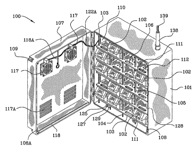
Fig. 1 is a front perspective view 100 of the intelligent power supply device
illustrating a plurality of removable cartridge energy packs 102 in a rack
residing
in an enclosure 101. The rack is best viewed in Figs. 1C, 1D, 1E and 1F.
Referring again to Fig. 1 the rack is not fully populated with batteries. The
removable cartridge energy packs 102 are preferably batteries and those shown
are
representative of a nominal 18 VDC Li-Ion cordless tool battery manufactured
and
sold by Makita . Makita is believed to be a trademark of Makita Corporation
of
Anjo-shi, Aichi-ken, Japan. Any type of battery may be used but Li-ion
(lithium
ion), NiMH (Nickel Metal Hydride), NiCd (Nickel Cadmium), Li-ion polymer,
lead acid or alkaline batteries are presently contemplated. Li-Ion is one
preferable
choice because of its gravimetric (energy per unit mass/weight) and volumetric
(energy per unit volume) efficiencies.
The United States Government (see 49 C.F.R. 173.185) and the United
Nations (see 4th Edition of the Manual of Tests and Criteria) places
restrictions
upon the transportation of certain lithium and lithium-ion batteries. Certain
lithium-ion batteries having a smaller capacity and therefore a lower lithium
or
equivalent lithium content are exempted from these restrictions. This becomes
an
advantage of the intelligent power supply design in that it preferentially
incorporates these smaller lithium-ion removable cartridge batteries.
CA 02642527 2008-08-07
WO 2007/092955 PCT/US2007/061928
Referring, again to Fig. 1, a partially populated rack is illustrated to
demonstrate that the power supply device will operate with at least one back-
up
battery 102. The batteries 102 may be removed at any time even while they are
in
operation and even while the power supply device is in operation. This is
known
as being hot swappable. Reference numeral 110 indicates a printed circuit
board
which contains 20 battery interface circuits thereon. Fig. 1 C is a front
perspective
view 100C of the rack illustrated in Figs. 1 and 1A and shows the back side of
the
printed battery interface circuit board 110 attached to the shelves 103 of the
rack
with screws 110A. Alternatively, the printed battery interface circuit board
may be
attached to the rack through the use of adhesives or by interlocking aspects
of the
circuit board and the shelves or rack implementing a "snap together"
construction.
Fig. lA is a front perspective view 100A of the power supply device similar
to Fig. 1 illustrating the power supply device without the removable cartridge
energy packs in the rack. It is anticipated that a user would wish to run the
intelligent power supply device without populating the rack with batteries
since in
fact, as explained herein, the power supply device is functional provided an
alternating current source and/or a direct current source is available. In
this mode,
the power supply can serve to transform power sources on behalf of the user.
For
example, a 230VAC 50Hz input can be usefully transformed by the intelligent
power supply into a 115VAC 60Hz output. See, Figs. 4, 4A, 4B and 4C. Still
31
CA 02642527 2008-08-07
WO 2007/092955 PCT/US2007/061928
referring to Fig. 1A, printed circuit board traces are indicated by reference
numeral
1lOB.
Referring to Figs. I and lA, shelves 103 are adapted to receive the Makita
18 VDC Li-Ion batteries 102. Shelves 103 may be made of an electrical
insulator
such as polycarbonate. Recesses 106 receive spring loaded locks 111, 112.
Reference is made to Fig. 1 J, a perspective illustration 100J of the
removable
cartridge energy pack/battery pack 102 manufactured by Makita and which is
illustrated in Fig. 1 et seq. Fig. 1K is a front view 100K of the removable
cartridge
energy pack/battery pack 102 and Fig. 1L is a side view 100L of the removable
cartridge energy pack/battery pack 102 illustrated in Fig. 1 et seq. Parts
labeled
111, 112 are integral such that as button 111 is depressed downwardly when
viewing Fig. 1 J against the force of an internal spring (not shown) tongue
112
recedes into the battery pack enabling insertion and withdrawal into the rack
which
is generally denoted by reference numeral 100C. In this way tongue 112 engages
the recess 106 of each shelf 103 and securely positions the battery into place
such
that it cannot be removed even if the enclosure 101 is accidentally or
purposefully
knocked over or subject to such shock and vibration as is typically present in
vehicle, aircraft, vessel, or spacecraft born applications.
Still referring to Figs. I and 1A, front door portion 107 is shown in the open
position exposing the interior of the enclosure 101 and the interior of the
door.
32
CA 02642527 2008-08-07
WO 2007/092955 PCT/US2007/061928
Door 107 can be securely locked and padlocked to protect the power supply
device
through known means. A threaded screw 109 is illustrated as one way to secure
the closure of the door.
Door 107 includes vents 117A which allow ventilation of the interior of the
enclosure when door 107 is closed. Filters may be placed over vents 1 17A to
protect from the intrusion of unwanted dust, debris, insects or other foreign
matters. Fans 117 located in the upper portion of the door 107 expel warmer
air
from the device creating negative pressure thus drawing cooler air in through
vents
11 7A. Duct or baffling elements (not shown) can be included to the effect of
directing cooler air entering via vents 117A first beneath battery rack lower
shelf
103 wherefrom it flows upward across motherboard 120 (figure 1B) before
traversing over top of the uppermost shelf and exiting via fans 117. In this
way
cooling of power conversion elements and other electronic and electrical
elements
housed on motherboard 120 is efficiently accomplished. Operation of the fans
117
is controlled by the microprocessor 495 based on various temperature
measurements. Wire harness 122A powers fans 117.
Still referring to Figs. 1 and lA, lip 118 is affixed to door 107 and is used
to
temporarily store the battery rack as illustrated in Fig. 1M. Fig. 1M a
perspective
view l OOM of the removable cartridge energy pack/battery pack rack removed
from the frame 101 of the intelligent power supply device and stored in the
door
33
CA 02642527 2008-08-07
WO 2007/092955 PCT/US2007/061928
107 enabling maintenance on the motherboard 120 in the rear of the device.
Loop
118A is used in conjunction with one of the threaded interconnecting rods 104
to
secure the rack in the door. Lip 118 secures another of the threaded
interconnecting rods 104. Door open sensor 108 interacts with block 108A on
door
107 to sense the position of the door. Door open sensor 108 is interconnected
to
the microprocessor as indicated in Fig. 4C. In Fig. 4C the door open sensor is
schematically illustrated using reference numeral 491.
Still referring to Fig. 1, wires 139 are illustrated in conduit 138
interconnecting with enclosure 101. Wires 139 include AC and DC inputs and
outputs and communication lines. As previously indicated, microprocessor 495
is
programmable over an Ethernet connection such that once the intelligent power
supply is fixed, for example, to a pole or other bulwark and electrically
connected
to a network access element such as a wireless access point via its Ethernet
connection, it may be re-programmed periodically to carry out different
algorithms
or operations depending upon the management systems' commands and
requirements.
Fig. 1B is a front perspective view 100B of the intelligent power supply
device without the rack 100C and without the removable cartridge energy packs
102 in the rack. Motherboard 120 is illustrated schematically in Fig. 1B and
includes, but is not limited to: input and output circuitry; the AC/DC
converter; the
34
CA 02642527 2008-08-07
WO 2007/092955 PCT/US2007/061928
DC/AC inverter; the first, second, third and fourth DC/DC converters; the
first,
second, third, intermediate and charge DC buses; the microprocessor;
interconnections between the microprocessor and the voltage and current
sensors
on all inputs and outputs; and, interconnections between the microprocessor
and
temperature sensors located in proximity to the converters.
Referring to Figs. 4, 4A, 4B and 4C, the microprocessor 495 makes voltage
measurements at all places indicated with a "V" having a circle around it.
Similarly, the microprocessor 495 makes current measurements at all places
indicated with an "I" having a circle around it. Similarly, the microprocessor
495
makes temperature measurements at all places indicated with,a "T" having a
circle
around it. It will be noticed that the temperature measurements are not
indicated as
being directly engaging any of the converters such as 406 and 414 for example
illustrated in Fig. 4. Rather, these temperature measurements are made by
sensors
on the motherboard in proximity to the device whose temperature is being
monitored. The sensors may be thermocouples, thermistors, platinum RTDs,
semiconductors (temperature sensor integrated circuits) or any other device
which
indicates a change in temperature as a function of voltage and/or current.
Voltage,
current and temperature interfaces (460, 461 and 462) are interposed between
the
microprocessor and the sensors. The microprocessor 495 may, for example, be a
Texas Instruments mixed signal microcontroller capable of analog to digital
CA 02642527 2008-08-07
WO 2007/092955 PCT/US2007/061928
conversion and digital to analog conversion and many other functions. Many
other
microprocessors may be used instead of the Texas Instruments mixed signal
microcontroller. An onboard and/or external timebase 463 will provide a
realtime
clock calendar so that time of day and date is known and it will provide a
high
resolution clock so as to make accurately timed measurements of system
operation.
Referring to Fig. 1B, a fastening bar 124 is affixed to the enclosure 101.
Another fastening bar not shown resides above the motherboard 120. First
and second connecting rods 125, 125A are affixed to the fastening bar 124
and extend outwardly therefrom toward the front of the device. Nuts 126 are
threaded and secured to the connecting rods 125, 125A to position the rack
(generally indicated as 110C) properly within the enclosure 110. Nuts 126
limit the rearward travel of the rack so that the rack does not engage or come
too close to the motherboard.
Still referring to Fig. 1B, communication and power wire harness 122 is
illustrated as extending from connector 121 to connector 123. Connector 123
joins
with connector 121A on the printed battery interface circuit board 110.
Alternatively, wire harness 122 may transmit power and communication signals
with the individual shelves 103A having battery interface circuits thereon.
See,
Fig. lI for the example of the battery interface circuits residing on the
shelves
103A. Gasket 128 protects the interior of the enclosure 101 from rain, snow,
other
36
CA 02642527 2008-08-07
WO 2007/092955 PCT/US2007/061928
forms of moisture such as salt and fresh water spray, dust, insects, and other
foreign and possibly degrading matter.
Referring to Figs. 1C shelves 103 having apertures 106 are shown in a
stacked relationship separated by hollow tube spacers 105. Fig. 11 is an
illustration
1001 of one of the shelves 103A of the rack having printed battery interface
circuits
(140, 141, 142, 143) on and in the shelf underneath the electrical
contacts/guides
131, 132. Guides/electrical contacts 131, 132 are "L"-shaped electrically
conductive and metallic and are adapted to interfit with the Makita battery
packs
102. Referring to Fig. 1J slots 112A, 112B engage electrical contacts 131, 132
and
include battery contacts (not shown) which conduct energy to and from the
battery
102. Referring to Figs. 1D, 1G and IF it will be noticed that the batteries
102 rest
upon one of the shelves 103 and are spaced apart from the next adjacent shelf
above the battery. Fig. 1 G is an enlargement of a portion 100G of Fig. 1D
illustrating one of the removable cartridge energy packs 102 in the rack and
illustrating the gap or space 150 between the battery and the shelf. A spring
loaded
lock 112 is illustrated residing in aperture 106 of the shelf in Figs. 1 G and
1H.
Figs. 1 D-1 H illustrate the example wherein wires 149 are used to transmit
power from the individual batteries (or other energy source) to the respective
battery interface circuit which is located on and in printed circuit board 110
as
illustrated in Fig. 1C, 1D and 1E. In the example illustrated in Figs. IC-IF
there
37
CA 02642527 2008-08-07
WO 2007/092955 PCT/US2007/061928
are 20 battery interface circuits on printed circuit board 110. Another
example (not
shown) houses the 20 battery interface circuits directly upon motherboard 120
with
the individual battery connections made via wires from each battery connector
location on each shelf to an appropriate connector associated with the battery
interface circuit housed upon the motherboard. Fig. 5 is a schematic 500 of
one of
the microprocessor-controlled interface circuits; each individual interface
circuit
controls one of the removable cartridge energy packs/battery packs 102, 202
(see,
Fig. 2) and the selective interconnection with the direct current energy
pack/battery
pack bus 450A, the charge bus 489A, the energy pack/battery pack monitor bus
495A and the energy pack/battery pack information bus 495B.
Fig. 1G is an enlargement of a portion 100G of Fig. 1D illustrating one of
the removable cartridge energy packs 102 in the rack. Fig. 1H is an
enlargement of
a portion 100H of Fig. 1F illustrating one of the removable cartridge energy
packs
102 in the rack. When reference is made to Figs. 1 G and 1 H, two of the wires
referred to by reference numeral 149 are viewed connected to threaded posts
131A
and 132A by nuts 131B and 132B. The threaded posts and corresponding nuts also
serve the function of securing the electrical contacts against the
polycarbonate
shelves. Posts 131A, 132A are viewed from above the shelves in Fig. 1C and
extend through the shelves and the guides/contacts 131, 132. It will also be
noticed from Fig. 1 C that an additional screw (unnumbered) is threaded into
the
38
CA 02642527 2008-08-07
WO 2007/092955 PCT/US2007/061928
guides/contacts to secure them to the polycarbonate shelf. Figs. 1 D and 1 E
illustrate the example where the temperature sensor 133 is located in
proximity to
the battery 102 and a wire(s) are connected to the sensor for communication
with
the battery interface circuit. All of the wires 149 are connected to
connectors 151
on the printed circuit board 110. Each shelf as viewed in Fig. 1 E includes 4
connectors for communication with the battery interface circuit.
Fig. lI is an illustration 1001 of one of the shelves 103A of the rack having
the battery interface circuits on and in shelf underneath the battery
contacts/guides.
In the example of Fig. 11, the shelves are made of material suitable for the
formation of printed circuits thereon, for example, glass reinforced epoxy
resin
material. Vertically extending connecting rods 104 run through bores 148 in
the
shelves 103 and hollow tube spacers 105 separate the shelves from each other.
Spacers 105 are stainless steel and sufficiently strong to support the
shelves.
Still referring to Fig. 11, a representative temperature sensor 144 which may
be any of those referred to above is located intermediate electrical contacts
131,
132 above the 18VDC Makita batteries. In this example the temperature sensor
is
part of the printed circuit board which resides underneath the electrical
contacts
131, 132. As stated previously, the Makita battery 102 is a dual use battery
wherein it may also be used in a cordless tool application. Other batteries
including user-defined batteries may be used in a wide range of voltages and
39
CA 02642527 2008-08-07
WO 2007/092955 PCT/US2007/061928
capacities. Batteries can be charged on board the rack 110C within the power
supply or on a separate charger not associated with the power supply device.
Alternatively, an entire rack of batteries may be removed from the power
supply
device and connected to a special purpose external charger designed to charge
any
and all of the batteries in the rack. Battery power is supplied to bus 450A
and
reference numeral 147 indicates system common. Temperature sensor information
is communicated using a battery information bus 495B. A charge bus 489A is
interconnected with each battery information circuit (140, 141, 142, 143)
printed
on the shelf 103A. Battery voltage information is communicated on battery
monitoring bus 495A and battery control information is communicated as
represented by line 495Z. Reference numera1495Z represents several discrete
control enable and disable channels grouped together in combination. In the
example of Fig. 11, a connector will be employed to communicate with another
printed circuit on board 110 which then communicates through connector 121A
back to the motherboard. Alternatively, each shelf 103A may communicate
directly back to a connector on the motherboard as described above in
descriptions
pertaining to Figs. 1D - 1H.
Referring to Figs. 1 C, 1 D, 1 E and 1 F, the top-most shelf 103 is held in
place
against the spacer 105 beneath it by nut 138. Other fasteners may be used to
hold
the shelves in place. Fig. 1D is a front view 100D of the rack partially
populated
CA 02642527 2008-08-07
WO 2007/092955 PCT/US2007/061928
with the removable cartridge energy packs 102 in the rack. Fig. 1E is a side
view
100E of the rack taken along the lines 1E-lE of Fig. 1D. Fig. 1F is a side
view
100F of the rack taken along the lines 1F-1F of Fig. 1D. Fastening bars 119
are
secured above the top-most shelf 103 and fastening bars 129 are secured
beneath
the bottom-most shelf. Each of the fastening bars 119, 129 include bores 119A,
129A therethrough for receiving rods 125, 125A which extend from bar 124
affixed to the enclosure 101. Additionally, fastening bars 119, 129 include
bores
which allow vertical threaded interconnecting rods 104 to pass therethrough.
Nuts
138, 139 secure bars 119, 129 to the shelves. With bars 119, 129 secured to
the
rack and with interconnecting rods 104/spacers 105 secured in place the rack
functions as a stable and rigid unit. Bars 119, 129 includes bores 119A, 129A
which allow passage of rods 125, 125A therethrough as well as other rods not
shown but described herein. Rods 125, 125A protrude from the end of bars 129
as
illustrated in Figs. 1 and 1A and nuts 127 are threaded onto rods 125, 125A to
secure the rack firmly in place within the enclosure 101.
Fig. 1N is a perspective view 100N a modular intelligent power supply
device having two intermediate fraines 152, 152A , each of which houses and
holds a rack housing a plurality of removable cartridge energy
packs/batteries. A
front cover 153 is hinged 155 to the first intermediate frame 152 and includes
ventilating fans and ports. The first intermediate frame 152 is hinged 154 to
the
41
CA 02642527 2008-08-07
WO 2007/092955 PCT/US2007/061928
second intermediate frame 152A. In turn, the second intermediate frame 152A is
hinged 156 to the rear cover 153A. Rear cover 163A includes a motherboard 160.
When fully populated the modular intelligent power supply device of the
example
of Fig. 1N provides twice the energy and power of the example illustrated in
Fig. I
fully populated.
Fig. 1N illustrates frame 152 being partially populated and employing
shelves 103A having the battery interface circuits printed on the underside
thereof.
Frame 152 may be partially populated because some of the batteries have been
removed for use in other applications such as on a cordless tool. Or, the
batteries
may have been removed for use in another power supply or they may have been
removed to enable charging on a separate stand-alone charger. It will be noted
that
the modular power supply device may be taken apart for maintenance by simply
removing the hinge pin(s) holding the frame of interest. One major advantage
of
the modular design is that it enables servicing of the motherboard while
maintaining (not interrupting) operation of the power supply system.
Fig. 2 is a front perspective view 200 of the intelligent power supply device
illustrating a plurality of removable cartridge energy packs 202 in a second
rack.
The other removable cartridge energy packs 202 illustrated are 28 VDC Li-Ion
batteries made by MilwaukeeOO, a registered trademark of Milwaukee Electric
Tool
Corporation of Brookfield, Wisconsin. The examples of Fig. 1 and Fig. 2
provide
42
CA 02642527 2008-08-07
WO 2007/092955 PCT/US2007/061928
approximately the same energy (nominally 1000 Watt-hours) and power (150
Watts) and weigh approximately 50 pounds. The example of Fig. 2 uses 12, 28
VDC Li-ion batteries. The example of Fig. 1N will provide approximately twice
the energy (nominally 2000 Watts-hours). Different power levels may be
possible
in any of the described configurations. A power level of 150 Watts may be
useful
for powering lighter loads such as mobile wireless routers or wireless access
points. A higher power level may be desirable for various transmitter or
transceiver communications gear, perhaps 300 to 400 Watts. These and other
power levels may be implemented via the use of appropriately sized AC/DC,
DC/DC, and DC/AC conversion units within the intelligent power supply. Larger
conversion units may require larger space within the power supply. Larger
space
may be achieved in the modular approaches of Figs. 1 or 1N by simply
increasing
the depth of the frame containing the motherboard or by increasing the width
and
height of all frame elements or both. Larger conversion units and higher power
levels may also require larger fans and greater cooling capacity. Larger fans
can be
accommodated easily in any of the described design approaches by increasing
the
depth of the fan and vent frame or by increasing the width and height of all
frames
or both. In this way, a very wide range in the amount of backup energy and the
power level of the supply can be achieved in appropriately scaled versions of
the
intelligent power supply.
43
CA 02642527 2008-08-07
WO 2007/092955 PCT/US2007/061928
Again referring to Fig. 1N, any number of intermediate frames may be added
to the modular power supply device to achieve the amount of backup energy
desired for a given application. In addition to the size of fans and vents
being
variable, the number of fans and vents may be increased to improve cooling
capacity as the number of intermediate frames is increased as well. Power to
operate the fans is provided by cabling as indicated by reference numeral
122A.
Power supplied to and from the battery racks housed in the intermediate frames
is
controlled by the battery interface circuits associated with each battery and
cable
122 provides transmission of that power to and from the motherboard 160. Cable
122 also transmits control signals from the microprocessor to each battery
interface
circuit. In the example of Fig. IN, fastening bars 119, 129 are fastened to
each of
the intermediate frames by mounts 158 or the like. Buckle type latches 157,
157A
may be padlocked for security purposes to prevent the theft of the power
supply
device or its components. The door open sensor 108 allows the microprocessor
to
be informed if a door is opened. Using a network connection to a management
system the microprocessor can then inform the management entity with a door
open event alarm and can differentiate tampering versus bona fide, scheduled
service so that management personnel can respond appropriately.
Fig. 2A is a front perspective view 200A of the intelligent power supply
device similar to Fig. 2 without the plurality of the other removable
cartridge
44
CA 02642527 2008-08-07
WO 2007/092955 PCT/US2007/061928
energy packs in the second rack. Similar reference numerals will be used in
connection with describing the example of Fig. 2. Fig. 2B is a front
perspective
view 200B of the second rack illustrated in Figs. 2 and 2A. Fig. 2C is another
front
perspective view 200C of the second rack illustrated in Figs. 2 and 2A.
Referring to Fig. 2, 28 VDC removable cartridge type batteries 202 are
illustrated in a partially populated rack affixed within enclosure 201. As
with the
example of Fig. 1 input and output power and communication wires 238 are
illustrated entering through an electrical conduit 238. The structural
arrangement of
the rack as identified generally by reference numerals 200B, 200C is
substantially
the same as the example of Fig. 1 only modified to accommodate the physically
larger batteries 202. Referring to Figs. 2B-2E, vertical connecting rods 204
pass
through bores in shelves 203. Spacers 205 reside over the vertical connecting
rods
204 and support and separate the shelves 203 from each other. Spacers 205 have
a
diameter larger than the diameter of the bars in the shelves 203. Fastener
bars 219,
229 include bores 219A, 229A therethrough for interconnection with rods 225,
225A for affixing the rack to the enclosure. Nuts 227 interengage the rods
225,
225A and secure the rack to the enclosure 201.There are additional bores
through
the fastener bars 219, 219A for interconnection with the vertically extending
connecting rods 204. The fastener bars 219, 219A are mounted above the top
shelf
and below the bottom shelf as illustrated. Rods 204 are threaded and in
conjunction
CA 02642527 2008-08-07
WO 2007/092955 PCT/US2007/061928
with nuts 238 and 239 provide a secure and stable rack which can be handled
without twisting and bending.
Door 207 operates to enable maintenance of the rack and the removal of the
batteries 202. The rack can be stored over lip 218 by using loop 218A to
secure
same and to enable maintenance on the motherboard. Fans 217, power cable
222A, vents 217A, door open switch 208A, and block 208 operates as was
explained above in connection with similar components Fig. 1. Gasket 228 keeps
unwanted rain and snow out of enclosure 201 and closure means 209 lock the
door
207 to the enclosure.
Referring to Figs. 2A et seq. printed battery interface circuit board 210B is
illustrated. Reference numera1210 is used to generally indicate the battery
interface circuit and it will be apparent to those of ordinary skill in the
art that the
printed battery interface circuits (one for each battery) may reside on either
the
inboard side or the outboard side of the board 210. Connector 221A and an
unnumbered cable are used to transmit power and control signals between the
battery interface circuits and the motherboard. Additional motherboard
connectors
are used if additional racks of batteries in additional frames are employed.
Fig. 2D is a front view 200D of the second rack partially populated with the
removable cartridge energy packs 202 in the second rack. Fig. 2E is a side
view
200E of the second rack taken along the lines 2E-2E of Fig. 2D. Fig. 2F is a
side
46
CA 02642527 2008-08-07
WO 2007/092955 PCT/US2007/061928
view 200F of the second rack taken along the lines 2F-2F of Fig. 2D.
Fig. 2G is an enlargement of a portion 200G of Fig. 2D illustrating one of
the removable cartridge energy packs 202 in the second rack. Fig. 2H is an
enlargement of a portion 200 H of Fig. 2F illustrating one of the removable
cartridge energy packs in the second rack. Battery 202 interconnects with a
Milwaukee connector 231 and is spaced above the shelf 203 as indicated by the
reference numeral 250. The Milwaukee 28 VDC battery 202 includes a locking
mechanism 211 which coacts with connector 231 to ensure that batteries are not
unintentionally removed from the rack. The Milwaukee connector includes two
lips 230, 231 which support battery 202 above the shelf 203. Connector 231 is
secured to the underside of shelf 203 with screws 231A, 232A as is best
illustrated
in Figs. 2B and 2C.
Fig. 21 is a perspective illustration 2001 of the removable cartridge energy
pack/battery pack 202 illustrated in Fig. 2. Fig. 21 illustrates a groove 231B
which
coacts with the lips on the connector 231 illustrated in Fig. 2G. Fig. 2J is a
front
view 200J of the removable cartridge energy pack/battery pack 202 illustrated
in
Fig. 2. Fig. 2K is a side view 200K of the removable cartridge energy
pack/battery
pack 202 illustrated in Fig. 2.
Fig. 2L is an example 200L of a power supply which includes a three by
three battery array 257 mounted in the rack 256 enclosed in weatherproof
cabinet
47
CA 02642527 2008-08-07
WO 2007/092955 PCT/US2007/061928
252 along with receptacles 255 and on-off switch 254 enclosed in weatherproof
electrical box 253. Electronics are indicated with reference numeral 258.
In addition to the battery packs referenced above supplied by Makita and
Milwaukee , other commercially available battery packs from other application
markets are anticipated and useable as backup energy sources within the power
supply. An example of such a battery pack would be the Digital DIONIC 160
power system offered by Anton Bauer, Inc. of Shelton, CT. In any case, a shelf
arrangement as depicted in FIG 1 and FIG 2 for specific battery pack types
would
be further adapted to enable use of the Anton Bauer or any other cartridge
style
energy pack.
Fig. 5 is a schematic 500 of one of the microprocessor-controlled battery
interface circuits. An interface circuit controls one of the removable
cartridge
energy packs/battery packs 102, 202 and the selective interconnection with the
direct current energy pack/battery pack bus 450A, the charge bus 489A, the
energy
pack/battery pack monitor bus 495A and the energy pack/battery pack
information
bus 495B.
Still referring to Fig. 5, the microprocessor 495 multiplexes voltage signals
from the battery monitor bus 495A and, as explained previously, is capable of
converting analog to digital signals. The microprocessor enables 495E the
voltage
48
CA 02642527 2008-08-07
WO 2007/092955 PCT/US2007/061928
monitoring of each of K batteries in the system according to clocked signals
(i.e.,
the timebase 463, see, Fig. 4C). The battery monitor bus is isolated from the
battery output/input 503 by two N-channel MOSFETs 519, 520. The monitor
enable 495E applies voltage across resistor 527 to the gate of N-channel
MOSFET
526 which, in turn, divides the battery voltage across resistor 525 in
proportion to
the combined resistance of resistors 524 and 525 and applies that voltage to
the
gate of P-channel MOSFET 521. P-channel MOSFET 521 then allows conduction
of current through resistors 522 and 523 dividing the voltage across resistor
523 in
proportion to the combined resistance of resistors 522 and 523 and applies
that
voltage to the gate of N-channel MOSFETs 519, 520 enabling the voltage to be
measured and sampled by the microprocessor 495. One exemplary P-channel
MOSFET which may be used is P channel Metal Oxide Semiconductor Field
Effect Transistor (MOSFET) made by International Rectifier. One exemplary N-
channel MOSFET which may be used is N-channel Metal Oxide Semiconductor
Field Effect Transistor nlade by Vishay Intertechnology, Inc. Other N-channel
and
P-channel MOSFETs may be used depending on the specific application.
Still referring to Fig. 5, the microprocessor 495 generates a charge enable
495D voltage across resistor 517 which drives the gate of N-channel MOSFET 516
which divides the charge bus 489A voltage across resistor 514 in proportion
the
combined resistance of resistors 514 and 515 which in turn enables P-channel
49
CA 02642527 2008-08-07
WO 2007/092955 PCT/US2007/061928
MOSFET 512 allowing the application of charge bus current to the battery 102,
202 by way of battery output/input 503. Charge bus 489A is isolated from the
battery output/input 503 by a diode. A representative diode which may be used
is
a Schottky Diode such as a l0A Dual Low Vf Schottky Barrier Rectifier made by
Diodes Incorporated. Wherever such Schottky Diode applications arise within
the
intelligent power supply, one may substitute an active diode oring circuit.
This
type of circuit prevents reverse current flow in the same way such flow is
blocked
by the diode. It has the further advantages of allowing forward current flow
with a
forward voltage drop which is substantially less than the diode. The active
oring
approach therefore provides diode functionality with reduced cost in terms of
system power. One exemplary implementation of the active oring alternative is
based upon a control IC such as International Rectifier's IR5001 s used in
conjunction with an appropriate N-channel MOSFET.
Still referring to Fig. 5, the microprocessor 495 multiplexes battery
information signals from the battery information bus 495B and, as explained
previously, is capable of converting analog to digital signals. Reference
numeral
501 indicates a voltage applied by a voltage regulator 497A. The
microprocessor
de-asserts an information disable signal 495F allowing current to flow through
resistor 528 and a light emitting diode 532A coupling the output of battery
102,
202 across resistor 530 in proportion to the resistance of 530 in proportion
to the
CA 02642527 2008-08-07
WO 2007/092955 PCT/US2007/061928
combined resistance of resistors 529 and 530 which drives the gate of N-
channel
MOSFET 531 effectively connecting the battery information bus 495B with a
battery information interface 530A to the effect of sensing one or more
parameters
about the battery such as temperature. The battery information interface may,
for
example, be a temperature sensor such as that denoted earlier by reference
numerals 133, 144. Alternatively, the battery information interface may
provide
access to a more or less complex communications protocol supported by a
particular type of battery or energy pack, such protocol being based upon
analog or
digital modulated or un-modulated physical signaling mechanisms in conjunction
with protocol software used to achieve higher levels of logical communications
between the microcontroller of the intelligent power supply and a peer process
or
controller within the battery or energy pack. This approach allows a very wide
range of information exchange including status information from the energy
pack
as well as control and command information to the energy pack to be
communicated. One known example of a communications protocol used in the
exchange of information with batteries is the SMBus. SMBus is the System
Management Bus defined by IntelO Corporation in 1995. SMBus or other possible
protocols may require multiple signals (e.g. clock and data signals). Although
only
one interface signal 531 is depicted in FIG. 5 it is intended that the battery
information bus 495B may be multiple signals in width and that additional
51
CA 02642527 2008-08-07
WO 2007/092955 PCT/US2007/061928
switches will be included as required to multiplex additional info bus signals
when
they are used.
In addition to the obvious benefits of accessing battery information via the
battery information bus 495B, the possibility to implement security and anti-
theft
functions are also important. In on scheme, energy packs (battery packs) would
be
disabled and unusable whenever they are outside of and independent of the
power
supply system. Using information secret to each power supply, and
communicating via the battery information bus 495B, the power supply would
selectively enable such energy packs only upon their insertion and recognition
by
the system. This would effectively thwart any motivation for theft of such
packs
(since they become useless once removed). Along similar lines, when the system
detects that a pack or packs have been removed as evidenced either by voltage
deficiency at the respective location on the battery monitor bus 495A or
cessation
of communications at the respective location on the battery information bus
495B,
the power supply can note such removals and report same as an alarm or
information event to its network management entities. Finally, the insertion
of
unauthorized or counterfeit packs may similarly be detected and reported.
Still referring to Fig. 5, reference numeral 501 is a voltage source from the
voltage regulator 497A and the microprocessor 495 generates a power enable
495C
voltage across resistor 511 voltage to drive the gate of N-channel MOSFET 507
52
CA 02642527 2008-08-07
WO 2007/092955 PCT/US2007/061928
allowing the division of battery voltage across resistor 510 in proportion to
the sum
of the resistance of resistor 509 and resistor 510. The divided voltage is
applied to
the gate of P-channel MOSFET 508 permitting conduction of current from the
battery output/input 503 to the direct current battery bus 450A. In general,
the
switching circuit just described using MOSFETs 507 and 508 in conjunction with
various resistors, voltage sources, and control signals is representative of
one
iinplementation for switching functions depicted in other parts of the figures
such
as elements 413 and 425 in Fig. 4 and even elements 550 and 550A in Fig. 5
itself.
Diode 505 permits forward current in the direction of the dc battery bus only
and
could be implemented at least using either the Schottky Diode or active oring
circuits mentioned previously in conjunction with the discussion surrounding
charge bus 489A.
Still referring to Fig. 5, a switch 550 is schematically indicated as
interconnected with Rsense bus 560. A Kth battery interface circuit is
illustrated as
being connected to the DC Battery Bus 450A to emphasize that there are K
battery
interface circuits. The Kth battery is also interconnected via switch 550A to
Rsense bus 560.
The structure and function disclosed herein can be used in automobiles and
other vehicles. Specifically, the structure and function of the instant
invention can
monitor the performance of a Lithium-ion powered automobile to determine the
53
CA 02642527 2008-08-07
WO 2007/092955 PCT/US2007/061928
performance of individual battery packs or individual battery cells within the
packs. This enables the clusters or groups of Lithium ion batteries to be used
in a
vehicle such that these clusters operate and function as a "gas" tank or more
appropriately as an "energy" tank. The microprocessor used herein notifies the
driver of the status of his energy tank thus informing the driver that it is
time to
refuel. The driver then stops at a service station where one or more of his
battery
packs is removed from his vehicle and exchanged with freshly charged battery
packs or groups or clusters of battery packs. The driver is given credit for
the
energy stored within his packs or clusters or groups of battery packs. In this
way
operation of battery powered electric vehicles becomes just like operation of
a
gasoline driven vehicle.
All of the switching (selectively coupling) performed by the battery interface
circuits is programmable with respect to operation of the rack of batteries
and also
with respect to other system inputs and outputs.
Fig. 7 is a schematic 700 illustrating up to K removable cartridge energy
packs/battery packs 701, 702, 703 selectively interconnected with N load buses
706, 707, 708, a sense resistor 603, an Rsense bus 560, a charge bus 489A and
a
monitor bus 495A. A plurality of switches 710 are shown each of which is
controlled by microprocessor 495. MCU 495 receives inputs as described
previously in connection with Fig. 5 and also receives inputs as indicated
54
CA 02642527 2008-08-07
WO 2007/092955 PCT/US2007/061928
scheinatically in connection with Figs. 4, 4A, 4B and 4C including voltage,
current, and temperature inputs. Fig. 7 also illustrates diodes 711 to inhibit
reverse
current flow with respect to each load bus 706, 707, 708 and the charge bus
489A.
The load buses 706, 707, 708 may be selectively disconnected from the load by
the
microprocessor.
Fig. 6 is a schematic 600 for obtaining load and removable cartridge energy
pack/battery pack 102, 202 information for use by the microprocessor 495.
Battery 102, 202 includes an energy source Vbat 607 and an internal resistance
Re
608. Monitor 602 measures the terminal output voltage across the battery 102,
202. The battery 102, 202 is selectively interconnected (coupled) by switch
604
with a user defined load or loads 601 and is also selectively interconnected
(coupled) by switch 605 with a sense resistor 603 of known resistance.
Still referring to Fig. 6, three measurement processes are implemented. In
the first process or first algorithm, the battery 102 is selectively connected
to and
disconnected from the user defined load 601 using switch 604. Voltage
measurements are made by the voltage monitor 602 with switch 604 closed to
obtain the voltage across the user defined load (Vcc-voltage closed circuit
user
defined load) and with the switch open to obtain the terminal output voltage
across
the battery 102 (Voc, voltage open circuit). In this process switch 605
disconnects
sense resistor 603 from the battery 102 at all times.
CA 02642527 2008-08-07
WO 2007/092955 PCT/US2007/061928
Still referring to Fig. 6, in the second process or second algorithm, the user
defined load 601 is selectively disconnected by switch 604 from the battery
102
while voltage measures are being taken. Voltage measurements are made by the
voltage monitor 602 with switch 605 closed (Vcc-sr, voltage closed circuit-
sense
resistor) and voltage measurements are made by the voltage monitor 602 with
the
switch 605 open (Voc, voltage open circuit).
Still referring to Fig. 6, in the third process or third algorithm, the user
defined load 601 is selectively connected to the battery by switch 604 at all
times.
Switch 605 is selectively connected to and disconnected from the sense
resistor
603 using switch 605. Voltage measurements are made across the sense resistor
603 in parallel with the user defined load Vcc(sr 11 ul)( voltage closed
circuit, sense
resistor 11 user defined load) when the switch 605 is closed. Voltage
measurements
are also made across the user defined load Vcc(ul)( voltage closed circuit-
user
defined load) when switch 605 is open.
In the first and second algorithms the closed circuit current, for example,
the
load current (Icc) may be obtained by:
(1) Vload=Vbat-Vrbat
where Vload = Vcc(ul)(voltage closed circuit-user defined load) or where
Vload=Vcc(sr)(voltage closed circuit-sense resistor) and Vrbat is the voltage
drop
across Re during the condition when Vload is established, and where Vbat=Voc,
56
CA 02642527 2008-08-07
WO 2007/092955 PCT/US2007/061928
substituting
(2) Voc-Vcc=Vrbat
assuming Rbat (Re) is known, dividing
(3) Vrbat/Rbat=lcc
Alternatively, assuming the load current, Iload, whether it be through the
user defined load (ul) or the sensor resistor load (sr), is known, then
(4) Re=(Voc- Vcc(ul)/Iload or, Re= (Voc - Vcc(sr))/Iload
In the third algorithm, Rbat (Re) and Rsense (Rs) are known from prior
determination. We measure Vcc(ul) (voltage closed circuit-user defined load)
and
Vcc(sr 11 ul) (voltage closed circuit, sense resistor 11 user defined load).
Icc(ul)
(current through the user defined load) is determined as follows:
(5) Vcc(ul)=Vbat*Rload/(Rload+Rbat)
and,
(6) Vcc(ul sr)=Vbat*(Rload 11 Rsense)/((Rload 11 Rsense) +Rbat), where
(7) Rload Rsense=Rload*Rsense/(Rload + Rsense), solving for Rload
(8) Rload= Rbat*(Vcc(ul)-Vcc(sr 11 ul)) /[Vcc(sr 11 ul) (1+Rbat/Rsense)-
Vcc(ul)], and, once Rload is known then the current through the load and the
battery can be determined by dividing Vcc(ul)/Rload=lload.
The current through the parallel combination of Rsense and Rload can be
calculated by:
57
CA 02642527 2008-08-07
WO 2007/092955 PCT/US2007/061928
(9) Icc(ul 11 sr) = Vcc(ul 11 sr)/(Road*Rsense/(Road + Rsense)
In the third algorithm, if the load current, Iload, through Rload is known by
measurement, then Rload can be calculated by:
(10) Vcc(ul)/Icc(ul)=Rload, and once Rload is known, then Rbat=Re can be
calculated from equation 8 if Vcc(ul), Vcc(sr ilul) and Rsense are known.
If the current through the user defined load is known and if the internal
resistance of the battery, Re, is known then a calculation of the voltage drop
across
the internal resistance of the battery can be made. Batteries, and in
particular Li-
Ion batteries, may be damaged if they are operated below a critical voltage
which
inferentially indicates that the state of charge is too low. Current flow
through the
battery, therefore, provides valuable information about the battery enabling
the
user or system to decide whether a measured terminal voltage is due to a high
load
or is due to a low state of charge operation. Li-Ion batteries which are
drained
below a protective state of charge may be permanently damaged. Therefore, the
microprocessor may selectively disconnect a particular back-up battery if its
state
of charge is too low. The microprocessor may decide to charge the particular
battery if its state of charge is approaching a critical value or the
microprocessor
may supply charge current which is summed with the current available from the
particular battery of interest and continue the contribution (albeit
diminished now
by the amount of the added charge current) of that battery as an energy
source.
58
CA 02642527 2008-08-07
WO 2007/092955 PCT/US2007/061928
If the discharge current through the load, Iload, is known or if the charge
current into a battery, Icharge, is known by a current measuring device then
Re can
be determined as indicated above. Re is important because it varies as a
function
of temperature, age, and other conditions of the battery and may indicate
trouble
with or end of life for the battery. Therefore, the microprocessor may
selectively
disable a particular back-up battery depending on a calculated Re, or the
microprocessor may signal an alarm event to inform the network management
entity of the inferred problem with a particular battery. An intermediate
possibility
exists wherein the microprocessor deploys or uses (connects to loads) each
battery
with a duty cycle proportional in some predictable way to the inferred health
of
each battery. For example, an older failing battery will be used seldom (but
not go
completely unused) compared to a brand new battery having maximal energy
which will be used often and preferentially. In this way, for a given
population of
K batteries in the system, the microprocessor may proceed to deploy these
batteries
in such a way that tends to equalize the health or electrical status of all.
Another
valuable function of the system rests on the microprocessor's ability, via the
measurelnents of voltage, current, and temperature, to estimate the absolute
capacity of each particular battery or energy source during a discharge
followed by
a charge cycle. The microprocessor can connect a particular battery to a load
until
such time as its state of charge is seen to be approaching 0% (fully
discharged).
59
CA 02642527 2008-08-07
WO 2007/092955 PCT/US2007/061928
From that point, the microprocessor can disconnect said battery from the load
and
connect said battery to the charge bus. The microprocessor can monitor the
current
over the time of charge of the particular battery until an appropriate charge
termination event such as a voltage or temperature event indicates completion
of
charge and arrival by the battery at the 100% state of charge level. The
record of
current multiplied by time increment during the charge cycle then indicates
the
electric charge imparted to the battery in the transformation from 0% to 100%
state
of charge. In the case of a coulombic efficient battery chemistry such as
lithium-
ion, the charge transferred will rather directly reflect the charge capacity
at 100%
state of charge. This capacity compared to the corresponding capacity of a
new,
unused battery will in turn reflect the age or conversely remaining useful
life of the
battery. For example, when the battery charge capacity at 100% state of charge
falls below 50% or the new charge capacity, the battery may be nearing the end
of
its useful life. In other cases where the chemistry is not 100% charge
efficient, the
100% state of charge energy will nonetheless provide insight and inference
into the
state of health of the battery. As mentioned earlier, in either case whether
the
battery chemistry is charge efficient or not, estimation of the inherent
resistance of
the battery (Re) in light of the prevailing temperature of the battery will
also
provide valuable inference into the state of health of the battery.
Fig. 4 is a schematic 400 illustrating an alternating current input 401
CA 02642527 2008-08-07
WO 2007/092955 PCT/US2007/061928
converted to a direct current by an AC/DC converter 406. The output 406A of
the
converter 406 is selectively switched by switch 407 to interconnect with a
direct
current intermediate bus 412B and/or is selectively switched by switch 408 to
a
second direct current bus 412A and/or is selectively switched to a third
direct
current bus 412C by switch 409. Output 406A of the converter is coupled via
connection 403 to the MCU 495 (see, Fig. 4C).
All of the elements indicated and described on Figs. 4, 4A, 4B and 4C are
mounted on the motherboard (printed circuit board). All of the elements are
scalable. For instance, one example of the system may provide 1000 Watt-hours
of
energy and can supply power nominally at 150 Watts. Another example may
supply 4000 Watt-hours of energy and can supply power at 800 Watts, etc.
Still referring to Fig. 4, diode 423 ensures that current flows from the
output
of the AC/DC converter to the direct current intermediate bus 412B but not the
reverse. Diodes 410 and 411 similarly ensure that current flows from the
output of
the AC/DC converter to the second direct current bus 412A and the third direct
current bus 412C, respectively, but inhibits flow in the reverse direction.
The AC
input is converted using AC detect 404 into a direct current voltage to which
microprocessor 495 is selectively coupled to measure allowing the voltage 405
of
the AC input to be thereby estimated. Current flowing through the AC input 401
is
sensed by a current detector and microprocessor 495 is selectively coupled to
61
CA 02642527 2008-08-07
WO 2007/092955 PCT/US2007/061928
measure the current 405A. The output 406A of the AC/DC converter is
selectively
coupled to the microprocessor to measure the voltage 412.
The AC/DC converter may for example be a 150 Watt enclosed single out
switcher capable of accepting 85-264 VAC input with a 24 VDC output,
manufactured by Cosel. Other AC/DC converters may be used which are capable
of converting a larger or smaller VAC input and are capable of producing much
higher or lower VDC outputs at much higher or lower wattage. Virtually any AC
input may be accepted by the power supply device and converter with a properly
selected converter.
Still referring to Fig. 4, the current output of the AC/DC converter 406 is
sensed and selectively coupled to the microprocessor to measure the current
412D.
A temperature sensor may be located on the motherboard in proximity to the
AC/DC converter and is selectively coupled with the microprocessor to measure
the temperature 412E.
The direct current bus may operate over a wide range of voltages and
currents as determined by user specifications and the requirements of a
particular
application. Typical voltages of the direct current intermediate bus 412 are
expected to be in the 12-30VDC range to enable supply of the intermediate bus
not
only from an AC/DC converter but also from back-up energy sources such as
removable cartridge direct current batteries which may or may not be dual
purpose
62
CA 02642527 2008-08-07
WO 2007/092955 PCT/US2007/061928
batteries.
Still referring to Fig. 4, the direct current intermediate bus 412B is
selectively interconnected by switch 413 to a direct current to alternating
current
converter 414 providing an alternating current output 417 and/or the direct
current
intermediate bus 412B is selectively coupled by switch 425 to a first direct
current
output 421 and/or the direct current intermediate bus is selectively coupled
via
switch 425A to a third direct current to direct current converter 427 to
provide
second 426 and third 428 direct current outputs. Voltage output 424, current
output 424A and temperature 424B of the direct current to direct current
converter
427 are monitored by the microprocessor. The input voltage 419 to the direct
current to alternating current converter is monitored by the microprocessor
495.
The alternating current output voltage 416 of converter 414 is converted by
detector 415 and monitored by the microprocessor, as is the output current
416A.
Temperature 416B of the direct current to alternating current converter 414 is
also
monitored by the microprocessor. The voltage 420 and current 420A of the first
421 direct current output are monitored by microprocessor 495.
The direct current to direct current converters may, for example be 10-32
VDC converters supplied by ACON. The AC/DC inverter may be a 150 Watt
inverter supplied by CD Media Corp.
When the phrase "monitored by the microprocessor" is used herein it means
63
CA 02642527 2008-08-07
WO 2007/092955 PCT/US2007/061928
that the microprocessor 495 converts a parameter such as voltage, current or
temperature from an analog to a digital signal and then processes that signal
data
according to a well defined algorithm.
Selective coupling or connection is accomplished by the microprocessor and
its control of the switches which interconnect the buses to the sources. As
described above, the output of the AC/DC converter is bused 406A to switches
407, 408 and 409 in parallel leading to respective buses. The microprocessor
controls switches 407, 408 and 409 (which may be implemented using P-channel
MOSFETS or other suitable electronic or mechanical switches) according to
system voltages, currents and temperatures of the inputs (including the back
up
batteries), outputs, buses, and converters according to pre-defined
programming or
specified manual control. For instance, there may be situations when the user
defines to preferentially use a particular input despite the availability of
other
inputs. An example may be a military application where it is decided to use
the
back up batteries as the energy source despite the availability of a direct
current
source from a vehicle so as to not deplete the batteries of the vehicle in a
combat
situation. As a further example, the microprocessor may infer from the level
of the
DC input representing the vehicle input whether or not the vehicle is running
and
correspondingly whether or not the vehicle's charging circuit is actively
supplying
current. With this information, the system can implement a control plan
wherein
64
CA 02642527 2008-08-07
WO 2007/092955 PCT/US2007/061928
the power supply load is sourced by the vehicle when it is running, by the
backup
batteries when the vehicle is not running, and then again by the non-running
vehicle battery after the backup batteries are depleted to a specified
1eve1(say 5%
state of charge). Finally, the load can be disconnected when both the vehicle
and
backup batteries have reached a pre-defined low state of charge. In this way,
the
intelligent power supply has maximized the run time of the load while
maintaining
the best disposition of vehicle reserve battery energy, and in the end, at
least
sufficient residual vehicle battery energy to guarantee the ability to start
the
vehicle.
Fig. 4A is a schematic 400A of a first 430 direct current input, a second 439
direct current input and a third direct current input 450A (battery pack
array) each
of which is selectively coupled to the direct current intermediate bus 412B,
and/or
the first direct current bus 412J and/or, the second direct current bus 412A
and/or
the third direct current bus 412C. The first direct current input 430 is bused
430A
and is selectively coupled by switch 431 with the direct current intermediate
bus
412B and/or is selectively coupled via switch 432 with the first direct
current bus
412J and/or is selectively coupled by switch 432A with the second direct
current
bus 412A and/or is selectively coupled by switch 433 with the third direct
current
bus 412C. Diodes 434, 435, 436, and 437 are located downstream from their
respective switches and ensure current flow from bus 430A to the respective
buses
CA 02642527 2008-08-07
WO 2007/092955 PCT/US2007/061928
and not the other way around. Voltage 438 and current 438A supplied by the
first
direct current input 430 is monitored by the microprocessor 495.
Third direct current input is a battery pack described herein above in regard
to Figs. 1, 2, 5, 6 and 7. An array of batteries arranged in parallel supplies
power
to bus 450B. The individual batteries may be of different individual voltages
and
chemistries and their use is controlled by the battery interface circuits
described
above employing a selective coupling system together with diode protection.
Still referring to Fig. 4A, the third direct current input 450A is bused 450B
and is selectively coupled by switch 451 with the direct current intermediate
bus
412B and/or is selectively coupled by switch 452 with the first direct current
bus
412J and/or is selectively coupled by switch 453 with the second direct
current bus
412A and/or is selectively coupled by switch 454 with the third direct current
bus
412C. Diodes 455, 456, 457, and 458 are located downstream from their
respective switches and ensure current flow from bus 450B to the respective
buses
but inhibit the reverse flow. The switches may be P-channel MOSFETs and the
diodes may be Schottky diodes. Voltage 459 and current 459A supplied by the
third direct current input 450A is monitored by the microprocessor 495. Each
of
the direct current inputs 430, 439, 450A. The AC/DC converter 406 and the
first
and second converters 475, 483 are protected against over-current and over-
voltage
conditions using devices such as fuses or PTC thermistor devices and Metal
Oxide
66
CA 02642527 2008-08-07
WO 2007/092955 PCT/US2007/061928
Varistars (MOVs) or other transient voltage suppression techniques.
Still referring to Fig. 4A, charge bus 489A is interconnected with the third
direct current input so as to enable selective recharging or load sharing as
described above in connection with Fig. 5, the battery interface circuit.
Still referring to Fig. 4A, the second direct current input 439 is bused
(439A)
and is selectively coupled by switch 440 with the direct current intermediate
bus
412B and/or is selectively coupled by switch 441 with the first direct current
bus
412J and/or is selectively coupled by switch 442 with the second direct
current bus
412A and/or is selectively coupled by switch 443 with the third direct current
bus
412C. Diodes 444, 445, 446, and 447 are located downstream from their
respective switches and ensure current flow from bus 439A to the respective
buses
but not in the reverse direction. The switches may be P-channel MOSFETs and
the
diodes may be Schottky diodes. Voltage 448 and current 448A supplied by the
third direct current input 450A is monitored by the microprocessor 495.
Still referring to Fig. 4A, third direct current bus 412C is coupled to fourth
direct current output 470 and its output voltage 470A and current 470B are
monitored by the microprocessor 495. The third direct current bus 412C may
also
be selectively coupled via switch 474 to the fourth direct current to direct
current
converter 473 which outputs to the fifth 471 and sixth 472 direct current
outputs.
Voltage 473A and current 473B and the temperature 473E of the converter 473
are
67
CA 02642527 2008-08-07
WO 2007/092955 PCT/US2007/061928
monitored by the microprocessor 495.
Fig. 4B is a schematic 400B illustrating the first direct current bus 412J
interconnected with a first direct current to direct current converter 475 and
the
output 475A of the first direct current to direct current converter 475
selectively
coupled to the direct current intermediate bus 412B and/or the third direct
current
bus 412C and/or the direct current charge bus 489A. The output bus 475A is
selectively coupled via switch 477 with the direct current intermediate bus
412B
and/or is selectively coupled via switch 478 with the third direct current bus
412C
and/or is selectively coupled via switch 479 with the direct current charge
bus
489A. Diodes 480, 480A, and 481 are located downstream from their respective
switches and ensure unidirectional current flow from bus 475A to the
respective
buses. The switches may be P-channel MOSFETs and the diodes may be Schottky
diodes. Voltage 482 and current 482A of the first direct current to direct
current
converter 475 as well as temperature 482E in the proximity of the converter
are
monitored by the microprocessor 495.
Still referring to Fig. 4B, the second direct current bus 412A is
interconnected with the input of a second direct current to direct current
converter
483 and the output 483A of the second direct current to direct current
converter
483 is selectively interconnected to the direct current intermediate bus 412B
and/or
the third direct current bus 412C and/or the direct current charge bus 489.
The
68
CA 02642527 2008-08-07
WO 2007/092955 PCT/US2007/061928
output bus 483A and is selectively coupled via switch 484 with the direct
current
intermediate bus 412B and/or is selectively coupled via switch 485 with the
third
direct current bus 412C and/or is selectively coupled via switch 486 with the
direct
current charge bus 489A. Diodes 484, 485, and 486 are located downstream from
their respective switches allowing current to flow from bus 483A only in the
direction of the respective buses 412B, 412C, and 489A. Once again, the
switches
may be P-channel MOSFETs and the diodes may be Schottky diodes. Voltage 490
and current 490A of the second direct current to direct current converter 483
as
well as temperature 490A in the proximity of the converter are monitored by
the
microprocessor 495. The charge bus 489A is interconnected with the removable
cartridge energy pack rack.
Again referring to Fig. 4B, it can be seen that microprocessor 495 has the
ability via converter output voltage control interface 495X to control the
output
voltage of DC/DC converter elements 475 and 483. The microprocessor can
decide, upon measuring the voltages and currents in different channels within
the
system, a best output voltage adjustment for each DC/DC converter such that
the
mix of power provided by each channel is thereby optimized according to some
pre-defined goal of the system. For example, a goal of utilizing 30% current
from
first DC input 430 along with 70% current from third DC input representing
backup batteries 450A can be realized by switching first DC input to power
first
69
CA 02642527 2008-08-07
WO 2007/092955 PCT/US2007/061928
DC/DC converter, switching third DC input to power second DC/DC converter,
and adjusting first DC converter voltage output and second DC converter
voltage
output up or down as required so that the current sensed at 482A compared to
the
current sensed at 490A are in the proportions 3:7. The scenario described is
one
from the category of control algorithms allowing intelligent power mixing. As
compared to an all or nothing contribution decision represented by a simple
switch,
power mixing allows a continuum of adjustments regarding how much power is
utilized from each source.
The converter voltage output control can be further understood by viewing
Fig. 52 signals DAC_DATA, DAC_SCLK, and DAC_SYNC_1 emanate from U34
MCU and go to Fig. 57 D 1 DAC (Digital to Analog Converter) U50 where four
analog voltage outputs are generated, DAC_DC 1_TRIM_1 through
DAC_DC4_TRIM_1. These signals route for amplification to respective amplifier
circuits U48, U49, U51, and U52. These amplifiers in turn generate voltage
control output signals DC1_TRIM_1 through DC4_TRIM_1. These signals
connect to the respective DCDC converter TRIM input pins on Fig 39 (DCDC1 U3
or U4) Fig. 41 (DCDC2 U5 or U6) Fig. 58 (DCDC3 U57) and Fig. 46 (DCDC4
U11).
Power mixing is important as one or more direct current to direct current
converters are arranged in an oring fashion. For example, a user defined
direct
CA 02642527 2008-08-07
WO 2007/092955 PCT/US2007/061928
current input source may be combined with the arrayed battery direct current
input
source comprising a plurality of batteries for the purpose of supplying one or
more
user selected loads in parallel. A first direct current to direct current
converter may
be coupled with the user defined direct current input source and a second
direct
current to direct current converter may coupled with the arrayed battery
direct
current input source, and, as just described the first and second converters
have
adjustable output voltages.
A microprocessor coupled to the first and second converters controls the
output voltages of the converters and the contribution of each of the direct
current
sources to the energy flowing on the DC bus(es) fed by both converters.
Secondly, the converters may be coupled together as illustrated in Fig. 4B
using
diodes such as Schottky diodes. Since the microprocessor measures the current
and voltage output by each converter as well as the current and voltage of the
respective inputs supplying said converters, it is possible for the
microprocessor to
adjust the output voltages of each converter to achieve several end goals
including
controlling the current, voltage, or power of each input, controlling the
current,
voltage, power, or temperature of each converter, and/or controlling the
current,
voltage, or power of the load bus(es). Finally, since the voltages of the
converters
are controlled according to net input, converter, or load characteristics
measured by
the microprocessor on a continuous basis, the control process will cancel out
71
CA 02642527 2008-08-07
WO 2007/092955 PCT/US2007/061928
varying characteristics such as forward voltage drop of the diodes or varying
characteristics of the converters of other components employed in the
circuits.
That is to say that the control process has the advantages of a closed loop
process
running to measured as opposed to predicted response variables.
The functions of measuring currents in the respective input, conversion, and
output channels is further illuminated. Shunt resistors are placed in the
negative
leg of the component whose current is to be measured, e.g. Fig. 46 U 11 pin 8
(VOUT Negative) connects to point DCDC4_OUT N. At Fig. 56 this signal
connects to GROUND via a shunt resistance formed by resistors R207 and R208 in
parallel (0.0025 ohms net). The small voltage developed across this shunt
resistance is proportional to the current flowing and is amplified in the
example by
differential amplifier formed around Op Amp U47. The output voltage from U47
is scaled suitably for measurement by the MCU Analog to Digital converter and
is
enabled onto the measurement bus for that purpose via an electronic switch
formed
by Q 108 and Q 109. In this way the MCU can determine the current in any of
the
"I" circled points (e.g. 490A, 482A) networked to the microprocessor interface
461
at any moment in time (see Figs. 4B and 4C).
Voltage measurements (e.g. 490, 482) are made similarly by appropriate
scaling by resistive voltage dividers and electronic switch multiplexing onto
an
ADC input channel of the MCU representing the interface 460 again in Figs 4B
72
CA 02642527 2008-08-07
WO 2007/092955 PCT/US2007/061928
and 4C.
Temperature measurements (e.g. 490E, 482E) are made similarly by using
NTC therlnistor devices in a voltage division network such that the voltage
measured by the MCU via another multiplexed ADC input channel represented by
interface 462 in Figs. 4B and 4C is proportional to the thermistor resistance
which
in turn is non-linearly indicative of the thermistor's temperature.
Exemplary modes of switch control are disclosed herein. The many system
switches such as those depicted in Figs. 4, 4A, 4B, 4C, and 5 are controlled
via
digital signals developed in the serial to parallel data conversion circuits
at Figs.
47-50. Using a few interface signals, the MCU can serially program these daisy
chained serial to parallel conversion circuits and cause their many parallel
outputs
to update to the desired control states (on or off, controlling whether
corresponding
switches are open or closed).
Fig. 4C is a schematic 400C illustrating the microprocessor 495, its power
supply (voltage regulator) 497A and interfaces. The voltage regulator 497A may
be a 3.3 VDC regulator from National Semiconductor. The voltage regulator
outputs 3.3 VDC to terminals represented by reference numeral 501 in Fig. 5,
the
battery interface circuit. The alternating current to direct current converter
403, the
first direct current input bus 430A, the second direct current input bus 439A,
the
third direct current input bus 450B and an independent replaceable battery 497
are
73
CA 02642527 2008-08-07
WO 2007/092955 PCT/US2007/061928
supplied in parallel to the voltage regulator to ensure power 497A and control
of
the power supply device. Voltage 496 of the battery is monitored by the
microprocessor to inform the user that battery 497 is low. Also schematically
indicated are interfaces 464, 465, 466, and 467 with a plurality of back-up
energy
subsystems which may be a rack of rechargeable batteries. Voltage 460, current
461 and temperatures from the individual components mounted on the mother
board are indicated as well as a time base for clocking measurements,
controlling
the switching and communicating internally and externally. The interface 495X
converter output voltage control interface which allows the microprocessor to
control and adjust the voltage (and thereby current) of each DC/DC converter
in
the system is also depicted.
Still referring to Fig. 4C, other inputs to the microprocessor includes a door
open sensor 491, power supply ambient temperature 492, status LEDs 494, fan
interface 498, serial interface 499 and Ethernet interface 499A. The serial
interface
may be used in conjunction with a service computer to interface to all status
and
control features of the intelligent power supply. Likewise, the Ethernet
interface
may be used for local interface and inquiries or may be used to connect the
intelligent power supply to a network whereby its management functions may be
implemented from client computers anywhere in the world having network access.
Switches 493 indicate globally the control of all switches on the motherboard
for
74
CA 02642527 2008-08-07
WO 2007/092955 PCT/US2007/061928
directing and routing power, and all switches for all of the battery interface
circuits. There may also be pushbutton or other user input switches which are
sensed and upon actuation responded to by the power supply controller.
Fig. 8 is an illustration 800 of the processing steps used in a configurable
microprocessor control algorithm including: measuring voltages and currents of
I
inputs, Q outputs, M buses, and K back-up batteries 801; measuring
temperatures
of L converters and K back-up batteries 802; analyzing measurements to
determine
optimal power switching 803; changing up to S switch states and V converter
output voltages as required to optimize power distribution 804, and
periodically
updating all measurements and repeating all of the steps 805.
Figs. 9A and 9B deserve in depth study as many of the features, benefits,
and potential uses of the scalable intelligent power supply invention are
depicted
therein. Scalable Intelligent Power Supply blocks are shown 901A through 906A,
each having a unique Internet Protocol (IP) address assigned as exemplified at
9061. The unique IP address coupled with the Ethernet interface shown at 499A
along with appropriate software contained in MCU 495 allows each power supply
to communicate in a network fashion with each other, other equipment such as
IP
peripherals such as 901C, 902C, or 903C, as well as management computers and
systems such as those depicted at 905B and 906B. This communications allows
information to be exchanged pertaining to the status or operating mode of the
CA 02642527 2008-08-07
WO 2007/092955 PCT/US2007/061928
power supplies or other equipment. For example, a status report screen is
depicted
schematically at network management computer 905B with related close up view
in 905H. 905H depicts a report originating from power supply 902A having IP
address 192.300.282.3. It can be seen that the status information includes
details
pertaining to the voltages, currents, temperatures, and utilizations as
applicable for
each input, converter, output, or battery within said power supply. That fact
that
this power supply is operating on behalf of seismometer 3 as well as its
location in
coordinates of latitude and longitude is also reported. This information is
beneficial to efficient management of the overall system as well as each
particular
node. Other computers including the management computer at 906B and ad hoc
computers such as laptops in the field can also access this information.
Appropriate security mechanisms including information encryption and password
protection are envisioned as an integral part of the intelligent power supply
system.
Several power supply use scenarios are depicted in Figs. 9A and 9B.
Scenario 1 at 901 depicts a power supply interfaced to a wireless router 901B
and a
video camera 901 C capable of transmitting video over Internet Protocol
(VOIP).
The interfaces include a power interface 901F to the VOIP camera and both a
power 901F and an Ethernet interface 901G to the wireless router whereby its
Internet Address 90 11 renders it reachable from anywhere on the Wide Area
Network (WAN) 908. The power supply is also interfaced to a street light 901D
76
CA 02642527 2008-08-07
WO 2007/092955 PCT/US2007/061928
whereby it receives input power via interface 901E. The specification for the
scenario contained in descriptive block 901 indicate that the combined load
requirements for the wireless router and the VOIP camera add up to 55 Watts.
The
output power type might be AC or DC voltages of appropriate levels depending
upon the requirements of the load devices. The scenario also specifies that
input
power from street light 901D will be intermittent, i.e., switched on 8 hours
and off
16 hours of each day. The power supply will therefore power the camera and
router from battery backup power for 16 hours while the street light power is
disabled (presumably during daylight hours) and will power the camera and
router
loads as well as recharge the backup batteries for 8 hours while the street
light
power is enabled. Should power fail unexpectedly during any interval, the
power
supply will switch instantly to backup battery power so that operation of the
loads
goes without interruption until input power is re-established. At all times,
the
power supply will measure and estimate the amount of backup energy available
and compare this to the amount it knows to be required for operation to
proceed
without interruption in the normal course of power cycling (8 hours on, 16
hours
off). It will be an important feature of the power supply system to be able to
predict energy deficiencies and subsequent power inadequacies and report same
as
an information or alarm event to its network management entities well in
advance
of such an event occurring. This report coupled with the capability of hot-
77
CA 02642527 2008-08-07
WO 2007/092955 PCT/US2007/061928
swappable battery packs will allow maintenance personnel to visit the location
in
advance of power running out and swap an adequate complement of worn batteries
for freshly charged ones to preclude the power failure.
Often peripherals such as the VOIP camera 901C involved in outdoor
deployments such as the street light scenario 901 will require ancillary
heating
under cold environmental conditions in order to maintain correct operation.
This
requirement is conventionally addressed with the addition of a heater device
which
would also be powered by the power supply. This increases the power level and
backup energy required in the power supply accordingly, an appropriate heater
costing an additiona120 to 30 Watts by way of example. The opportunity arises,
with the intelligent power supply, to accomplish the requirement for ancillary
heat
more efficiently. In particular, heat is generated inside the power supply as
a result
of operation of voltage conversion units, charging of batteries, and power
dissipation in the electronic and electrical components of the power supply
system
in general. If the power supply is connected via a duct or conduit such as
that
schematically depicted by 901J, air warmed within the power supply by
aforementioned phenomenon may be conveyed to the peripheral device requiring
ancillary heat. The ducting may be accomplished coaxially in the conduit
already
positioned to convey the power cables or may occur via a separate conduit
placed
expressly for the heating purposes. A fan inside the power supply, controlled
by
78
CA 02642527 2008-08-07
WO 2007/092955 PCT/US2007/061928
MCU 495, may be used to produce the desired air flow. The power supply may
control the amount of warm air, if any, based upon its measurement of external
temperature, its measurement of its internal air temperature, and
communications
of information via its Ethernet connection with either the peripheral
requiring heat
and/or its network management systems.
Scenario 2 at 902 depicts what might be instrumentation (seismometer
902C) deployed in a sunny, remote location such as the American southwest
desert. In this case power supply 902A powers the seismometer 902C as well as
a
wireless network access device 902B. Power will be available to the power
supply
via solar panel 902D, ordinarily over the course of 12 hours of daylight only.
During the dark periods the power supply must operate from its backup energy
sources. Cloudy days may occur when the "dark period" is extended from 12 to
perhaps 48 or more hours. Therefore, a typical deployment may utilize
additional
backup energy frames such as those depicted in FIG 1N to achieve the requisite
backup energy reservoir needed for prolonged, input-power-deprived operation.
Scenario 903 depicts a mobile, vehicle born application wherein power
supply 903A derives input power from vehicle 903D when available, charging its
backup energy sources and powering its loads including network access device
903B and Voice over IP telephone 903C. The power supply may be programmed
to be cognizant of the state of the vehicle power system. The MCU 495 may
infer
79
CA 02642527 2008-08-07
WO 2007/092955 PCT/US2007/061928
from voltage measurements of the DC input coming from the vehicle whether or
not the vehicle is running and actively charging its own battery. In the case
where
the vehicle is running, its power may be the preferred source. In the case
where the
vehicle is not running, it may be preferred to power the loads from the backup
energy sources within the power supply thus preserving the vehicle battery
maximally. It may also be possible to remove (disconnect) from the vehicle
altogether and transport the power supply along with it wireless router and
telephone to a different location, perhaps another vehicle or outpost having a
different power source available. It may then be possible to reconnect the
power
supply to a new power source when available and re-charge any backup energy
that was used in the transition between power sources all the while operating
the
network interfaces and telephone (or other peripherals) without interruption.
Scenarios 904, 905, and 906 depict power supply applications wherein input
power is provided by a dedicated, full time AC outlet. The only interruptions
expected are those interruptions that occur on occasion in the utility grid
(black out
or brown out events). These interruptions may be infrequent and of typically
short
duration. Therefore, it is possible that the backup energy required in these
power
supplies 904A, 905A, and 906A may be substantially less than that required in
the
previously described scenarios. The advantage of the scalable power supply
architecture would then allow few backup energy packs to be populated (a
partial
CA 02642527 2008-08-07
WO 2007/092955 PCT/US2007/061928
rack full) and therefore allow a lower cost for the required system.
Alternatively,
one or more of the fixed computers or network interfaces may desirably have
extended backup time to cover an extended power outage. The precise number of
energy packs and/or the desired number of frames of power packs may be applied
to each node as desired or required on a node-by-node energy/backup time
requirement basis. Finally, it may be possible that power outages may exceed
the
interval for which backup power has been designed. The power supply has the
advantages of being able to accurately predict the amount of backup power
remaining, communicate anticipated backup energy deficits well in advance via
its
network interface, and remain functional for additional extended periods by
the
mechanism of hot swapping energy packs via maintenance intervention.
Figure 10 illustrates exemplary power supply generation circuits wherein
reference numeral 1001 indicates a negative 3.3V supply and reference numeral
1002 indicates a positive 6.6V supply.
Figure 11 illustrates exemplary microprocessor-controlled battery interface
circuits, detailed example, (1 of 20). Reference numeral 1101 is the discharge
control switch circuitry, as described in connection with Fig. 5 above. Charge
control switch circuit 1102 is shown in exemplary fashion and has been
described
in connection with Fig. 5 above. Battery monitor bus multiplex circuit 1103
has
been described above in connection with Fig. 5. And, battery information bus
81
CA 02642527 2008-08-07
WO 2007/092955 PCT/US2007/061928
switch circuit 1104 has been described above as well in connection with Fig.
5.
Connector 1105, by which battery bus and switch control signals are connected
with other system elements including the microprocessor and power conversion
units, is illustrated in Fig. 11. Figures 12 through 30, are exemplary of
battery
interface circuits like the one just described in connection with Fig. 11 and
Fig. 5.
Reference numerals 1200, 1300, 1400, 1500, 1600, 1700, 1800, 1900, 2000, 2100,
2200, 2300, 2400, 2500, 2600, 2700, 2800, 2900 and 3000, illustrate the
nineteen
additional microprocessor-controlled battery interface circuits. Any number of
battery interface circuits may be employed.
The circuitry and control methodology described herein is equally applicable
to use of modular energy supply systems in automobiles. For instance, the
control
methodology described herein may be used in connection with Lithium ion
batteries used in an automobile. In this way, the batteries may be removed
from
the automobile and recharged at a service station and then replaced into the
vehicle
fully charged. The batteries may be separately removed from the automobile or
they may be removed in groups. The invention as taught and described herein
enable the evaluation of individual batteries and the evaluation of the energy
remaining in the batteries at the time they are swapped out (exchanged) for
fully
charged batteries. In this way a motorist can effectively refuel his or her
vehicle
and proceed on his or her way without worrying about stopping to charge the
82
CA 02642527 2008-08-07
WO 2007/092955 PCT/US2007/061928
batteries which is time consuming as the recharge time for Lithium ion
batteries is
considerable. Having the ability to quickly swap the batteries in a Lithium
ion car
enables the driver to get credit for the energy in his "gas" tank. In reality
the
teachings of the instant invention enable the driver to effectively have an
"energy
tank" as compared to a "gas tank."
Fig. 31 illustrates 3100 exemplary AC input and AC/DC converter circuits
which are described elsewhere hereinabove in connection with Figs. 4, 4A, 4B,
4C
and 5. Reference numeral 3101 indicates input terminals for AC line, neutral,
and
ground. Reference numeral 3102 indicates an AC input fuse which protects
converter 406. Reference numeral 3103 is an AC input transient voltage
suppression circuit protecting converter 406. Reference numeral 3104 is an
indication of an AC detect circuit, as described elsewhere referring to Fig.
4,
reference numerals 404, 405. Reference numeral 3105 indicates in an exemplary
fashion AC/DC converter, as described elsewhere referring to Fig. 4, reference
numeral 406. Reference numeral 3106 is exemplary of AC/DC temperature
sensing circuit, as described elsewhere referring to Fig. 4, reference numeral
412E.
Reference numeral 3107 indicates AC/DC converter DC output voltage selective
coupling as described elsewhere referring to Fig. 4 (reference numerals 406A
and
412).
Fig. 32 illustrates 3200 exemplary AC/DC converter DC output voltage bus
83
CA 02642527 2008-08-07
WO 2007/092955 PCT/US2007/061928
connection switches. Selective coupling circuits 3201 are illustrated for
AC/DC to
DC INT BUS, as described elsewhere referring to Fig. 4 (reference numerals
406A,
407, 423, and 412B). Selective coupling circuits 3202 for coupling the AC/DC
to
SECOND DC BUS as set forth and previously described in connection with Fig. 4
(406A, 408, 410, and 412A). And, selective coupling circuits 3203 for coupling
the AC/DC to THIRD DC BUS, as described elsewhere referring to Fig. 4
(reference numerals 406A, 409, 411, and 412C).
Fig. 33 illustrates 3300 First DC input circuits wherein reference numeral
3301 indicates DC input terminals for positive, negative, and ground and
reference
numeral 3302 DC indicates an input fuse. DC input transient voltage
suppression
circuit 3303 is illustrated as an MOV. DC input voltage monitoring selective
coupling circuit 3304 is illustrated and was described elsewhere referring to
Fig.
4A (reference numeral 438).
Fig. 34 illustrates 3400 the First DC input bus connections switches in
exemplary fashion and as described elsewhere referring to Fig. 4A. Selective
coupling circuits 3401 for coupling first DC input to second DC bus (Fig. 4A,
reference numerals 430A, 432A, 436, 412A) are illustrated in Fig. 34 as are
the
selective coupling circuits 3402 for coupling the first DC input to third DC
bus
(Fig. 4A, reference numerals 430A, 433, 437, 412C). Fig. 34 also depicts
selective
coupling circuits 3403 for the first DC input to DC INT bus as described above
in
84
CA 02642527 2008-08-07
WO 2007/092955 PCT/US2007/061928
connection with Fig. 4A, reference numerals 430A, 431, 434, 412B.
Selective coupling circuits 3404 for coupling the first DC input to the first
DC bus are illustrated in Fig. 34 and also as described above in connection
with
Fig. 4A, reference numerals 430A, 432, 435, 412J.
Fig. 35 illustrates 3500 the Second DC input circuits wherein reference
numeral 3501 DC indicates the input terminals for positive, negative, and
ground
and reference numeral 3502 indicates the DC input fuse. Reference numeral 3503
indicates the DC input transient voltage suppression circuit (MOV) and
reference
numeral 3504 illustrates the DC input voltage monitoring selective coupling
circuit
as described above referring to Fig. 4A, reference numeral 448.
Fig. 36 illustrates 3600 exemplary Second DC input bus connection
switches, as described above referring to Fig. 4A. Selective coupling circuits
3601
for coupling the second DC input to second DC bus are illustrated in Fig. 36
and
have been described previously in Fig. 4A, reference numerals 439A, 442, 446,
412A. Selective coupling circuits 3602 for coupling second DC input to third
DC
bus are illustrated in Fig. 36 in exemplary fashion and are discussed above in
connection with Fig. 4A, reference numerals 439A, 443, 447, 412C. Selective
coupling circuits 3603 for coupling the second DC input to DC INT bus are
illustrated by way of example in Fig. 36 and were discussed above in
connection
with Fig. 4A, reference numerals 439A, 440, 444, 412B. And, selective coupling
CA 02642527 2008-08-07
WO 2007/092955 PCT/US2007/061928
circuits 3604 for coupling the second DC input to the first DC bus are
illustrated by
way of example in Fig. 36 and are discussed above in connection with Fig. 4A,
reference numerals 439A, 441, 445, 412J.
Fig. 37 illustrates 3700 the Third DC input battery pack array circuits
wherein reference numeral 3701 indicates DC input fuse and reference numeral
3702 indicates DC input transient voltage suppression circuit as described
above as
an MOV. DC input voltage monitoring selective coupling circuit 3703 is also
depicted in Fig. 37 and is described elsewhere described elsewhere in Fig. 4A,
reference numeral 459.
Fig. 38 illustrates 3800 the Third DC input bus connections switches
described above in connection with Fig. 4A wherein selective coupling circuits
3801 couple the third DC input with the second DC bus, Fig. 4A, reference
numerals 450B, 453, 457, 412A. Also shown in Fig. 38 are the selective
coupling
circuits 3802 for coupling the third DC input to third DC bus as described
above in
connection with Fig. 4A, reference numerals 450B, 454, 458, 412C. Selective
coupling circuits 3803 for coupling the third DC input to DC INT bus as
described
above in connection with Fig. 4A, reference numerals 450B, 451, 455, 412B and
selective coupling circuits 3804 for coupling the third DC input to first DC
bus are
shown in Fig. 38 and were previously described above in connection with Fig.
4A,
reference numerals 450B, 452, 456, 412J.
86
CA 02642527 2008-08-07
WO 2007/092955 PCT/US2007/061928
Fig. 39 illustrates 3900 the First DC/DC converter circuits 3901 described
above in Fig. 4B (reference numeral 475) wherein First DC/DC converter
temperature measuring circuit 3902 was described in Fig. 4B in connection with
reference numeral 482E. Alternative first DC/DC converter 3903 having a
detailed
pin assignment differing from 3901 is also illustrated in Fig. 39. DC/DC
converter
voltage monitoring selective coupling circuit 3904 described in connection
with
Fig. 4B, reference numeral 482 and is illustrated in Fig. 39.
Fig. 40 illustrates 4000 the First DC/DC converter bus connections switches
described in connection with Fig. 4B wherein selective coupling circuits 4001
for
coupling the first DC/DC converter to DC INT bus were described in connection
with reference numerals 475A, 477, 480, 412B. Selective coupling circuits 4002
for coupling the first DC/DC converter to third DC bus are illustrated in Fig.
40
and were described above in connection with Fig. 4B, and in particular with
reference numerals 475A, 478, 480A, 412C. Selective coupling circuits for 4003
for coupling the first DC/DC converter to the DC charge bus are illustrated in
Fig.
40 and were described above in connection with Fig. 4B, reference numerals
475A,
479, 481, 489A.
Fig. 41 illustrates 4100 the Second DC/DC converter circuits 4101 described
elsewhere referring to Fig. 4B (reference numeral 483) and the Second DC/DC
converter temperature measuring circuit 4102 as described elsewhere referring
to
87
CA 02642527 2008-08-07
WO 2007/092955 PCT/US2007/061928
Fig. 4B (reference numeral 490E). Alternative second DC/DC converter 4103
having a detailed pin assignment differing from 4101 is illustrated in Fig. 41
as
well. DC/DC converter voltage monitoring selective coupling circuit 4104 as
described elsewhere referring to Fig. 4B (reference numeral 490) is also
illustrated
in Fig. 41.
Fig. 42 illustrates 4200 in exemplary fashion the Second DC/DC converter
bus connections switches described in Fig. 4B wherein the selective coupling
circuits 4201 for coupling the second DC/DC converter to DC INT bus. See the
discussion of Fig. 4B as it pertains to reference numerals 483A, 484, 487,
412B.
Selective coupling circuits 4202 for coupling the second C/DC converter to
third
DC bus as described in above in connection Fig. 4B and reference numerals
483A,
485, 488, 412C are shown in Fig. 42. Also, selective coupling circuits 4203
for
coupling the second DC/DC converter to DC charge bus are shown in Fig. 42 and
were discussed above in connection with Fig. 4B, reference numerals 483A, 486,
489, 489A.
Fig. 43 illustrates 4300 the DC/AC inverter circuits wherein the DC/AC
inverter input power switch 4301 as described elsewhere referring to Fig. 4,
reference numeral 413, and DC/AC inverter 4302 as described in Fig. 4,
reference
numeral 414 are shown. DC/AC inverter temperature measuring circuit 4303 is
also illustrated in Fig. 43 and previously described referring to Fig. 4,
reference
88
CA 02642527 2008-08-07
WO 2007/092955 PCT/US2007/061928
numeral 416B.
Still referring to Fig. 43, DC/AC inverter output terminals 4303 for line,
neutral, and ground are shown as is the DC/AC inverter output fuse 4305. DC/AC
inverter output transient voltage suppression circuit 4306 is illustrated in
Fig. 43 as
an MOV and was described previously. DC/AC inverter AC detect circuit 4307 is
illustrated in Fig. 43 and was described above in regard to Fig. 4, reference
numeral 415 and 416.
Fig. 44 illustrates 4400 the First DC output circuits wherein the First DC
output switch 4401 was described elsewhere referring to Fig. 4, reference
numeral
425. First DC output terminals 4402 for positive, neutral, and ground are
shown in
Fig. 44 as is the First DC output fuse 4403. First DC output transient voltage
suppression circuit 4404 is an MOV as was previously described above. First DC
output voltage monitoring selective coupling circuit 4405 is illustrated in
Fig. 4
and described above in connection with Fig. 4, reference numeral 420. DC/AC
inverter input voltage monitoring selective coupling circuit 4406 is also
illustrated
in Fig. 44 and was described hereinabove in connection with Fig. 4, reference
numeral 419.
Fig. 45 illustrates 4500 the Third DC bus and fourth DC/DC converter
circuits wherein the Third DC bus voltage monitoring selective coupling
circuit
4501 as described elsewhere referring to Fig. 4A, reference numeral 470A.
Fourth
89
CA 02642527 2008-08-07
WO 2007/092955 PCT/US2007/061928
DC/DC converter input voltage switch 4502 is disclosed in Fig. 45 as described
elsewhere referring to Fig. 4A, reference numeral 474. Fourth DC/DC converter
output voltage monitoring selective coupling circuit 4503 as described
elsewhere
referring to Fig. 4A, reference numeral 473A.
Figure 46 illustrates 4600 the fourth, fifth, and sixth DC outputs and fourth
DC/DC converter circuits wherein the Fourth DC output terminals for positive,
neutral, and ground 4601 and the Fourth DC output fuse 4602 are illustrated.
The
Fourth DC output transient voltage suppression circuit 4603 is an MOV and the
Fifth DC output terminals 4604 for positive, neutral, and ground are also
illustrated
in Fig. 46. Fifth DC output fuse 4605 and the Fifth DC output transient
voltage
suppression circuit 4606 which is an MOV are illustrated in Fig. 46. Fourth
DC/DC converter 4607 and Sixth DC output 4608 as described elsewhere referring
to Fig. 4A , reference numeral 473 and 472, respectively, are also illustrated
in Fig.
46. And, Fourth DC/DC converter temperature measuring circuit 4609 is
illustrated
in Fig. 46 and was illustrated previously in Fig. 4A as reference numeral
473E.
Fig. 47 illustrates 4700 serial to parallel circuits to implement serial
microprocessor control instructions into parallel control signals wherein
power
supply decoupling capacitors 4701 for the respective integrated circuits are
shown.
Serial to parallel converters 4702 are also illustrated in Fig. 47.
Figs. 48-50, reference numerals 4800, 4900, 5000, illustrate additional serial
CA 02642527 2008-08-07
WO 2007/092955 PCT/US2007/061928
to parallel circuits implementing the microprocessor control signals.
Fig. 51 illustrates 5100 Microcontroller interface circuits wherein the
temperature measuring circuit interface 5101 to the microcontroller is shown
and
was described elsewhere referring to Fig. 4C, reference numeral 462. Reference
numeral 5102 indicates the battery monitor bus circuit interface to
microcontroller
as described elsewhere referring to Fig. 5, reference numeral 495A. Reference
numeral 5103 indicates a voltage monitor circuit interface to the
microcontroller as
described elsewhere referring to Fig. 4C, reference numeral 460. The current
monitor circuit interface 5104 to the microcontroller is shown in Fig. 51 and
is
described elsewhere referring to Fig. 4C, reference numeral 461. And,
reference
numeral 5105 indicates the serial interface to microcontroller as described
elsewhere referring to Fig. 4C, reference numeral 499.
Fig. 52 illustrates 5200 the Microcontroller and support circuits. Reference
numeral 5201 indicates the voltage regulator and power supply for the
microcontroller as described elsewhere referring to Fig. 4C, reference
numerals
403, 430A, 439A, 450B, 497A and 497. The Microcontroller unit is indicated as
reference numeral 5202.
Fig. 53 illustrates 5300 the Microcontroller interface circuits wherein door
switch interface circuit 5301 to the microcontroller is shown and was
described
elsewhere referring to Fig. 4C, reference numeral 491. Reference numeral 5302
91
CA 02642527 2008-08-07
WO 2007/092955 PCT/US2007/061928
represents a light emitting diode interface circuit to the microcontroller as
was
described elsewhere referring to Fig. 4C, reference numeral 494. Dual cooling
fan
control circuits interface 5303, 5304 to the microcontroller are shown and
were
described elsewhere referring to Fig. 4C (498).
Fig. 54 illustrates 5400 current monitoring circuits in an exemplary fashion.
Reference numeral 5401 indicates the current monitor interface for third DC
input
battery pack array as described elsewhere referring to Fig. 4A, reference
numeral
495A. Reference numeral 5402 indicates the current monitor interface for the
first
DC input as described elsewhere referring to Fig.4A, reference numeral 438A.
Current monitor interface 5403 for second DC input is also shown in Fig. 54
and
was previously described above referring to Fig. 4A, reference numeral 448A.
Current monitor interface 5404 for AC/DC converter output is indicated in Fig.
54
as well and was described elsewhere referring to Fig. 4, reference numeral
412D.
Fig. 55 illustrates 5500 the current monitoring circuits wherein the current
monitor interface for the first DC/DC converter 5501 is shown and was
described
elsewhere referring to Fig. 4B, reference numeral 482A. Reference numeral 5502
indicates the current monitor interface for the second DC/DC converter and was
described elsewhere herein in regard to Fig. 4B, reference numeral 490A.
Reference nutnera15503 indicates current monitor interface for DC/AC inverter
input as was described elsewhere referring to Fig. 4, reference numeral 416A.
92
CA 02642527 2008-08-07
WO 2007/092955 PCT/US2007/061928
Fig. 56 illustrates 5600 a current monitoring circuits wherein reference
numeral 5601 indicates the current monitor interface for first DC output as
described elsewhere referring to Fig. 4, reference numeral 420A. Current
monitor
interface 5602 for the second DC output as described elsewhere referring to
Fig. 4
Reference numeral 5603 indicates the current monitor interface for third DC/DC
converter as described elsewhere referring to Fig. 4, reference numeral 424A
and
reference numeral 5604 indicates the current monitor interface for fourth
DC/DC
converter as described elsewhere referring to Fig. 4A, reference numera1473B.
Fig. 57 illustrates 5700 the DC/DC converter voltage programming circuits
wherein reference numeral 5701 indicates the voltage programming circuit for
the
first DC/DC converter as described elsewhere referring to Fig. 4B, reference
numeral 495X. Voltage programming circuit 5702 for the third DC/DC converter
is
illustrated in Fig. 57 and was described elsewhere referring to Fig. 4B,
reference
numeral 495X. Reference numeral 5703 is the voltage programming circuit for
the
second DC/DC converter as described elsewhere referring to Fig. 4B, reference
numeral 495X. Reference numeral 5704 indicates the voltage programming circuit
for the fourth DC/DC converter as described elsewhere referring to Fig. 4B,
reference numeral 495X. And, reference numeral 5705 indicates the digital to
analog converter used to generate voltage programming levels.
Fig. 58 illustrates 5800 the second and third DC outputs and third DC/DC
93
CA 02642527 2008-08-07
WO 2007/092955 PCT/US2007/061928
converter circuits in an exemplary fashion wherein the Third DC/DC converter
input voltage switch 5801 is shown and was described elsewhere referring to
Fig.
4, reference numeral 425A. The Third DC/DC converter voltage monitoring
selective coupling circuit 5802 is also shown in Fig. 58 and was described
elsewhere referring to Fig. 4, reference numera1424. Third DC/DC converter
5803
is shown as well in Fig. 58 and was described elsewhere referring to Fig. 4,
reference numeral 427. Second DC output terminals 5804 are indicated as well
for
positive, neutral, and ground (426). Also shown is the Second DC output fuse
5805
and the Second DC output transient voltage suppression circuit 5806 which is
an
(MOV). Third DC output 5807 (Fig. 4, reference numeral 428). Third DC/DC
converter temperature measuring circuit 5808 is also shown in Fig. 58 and was
described elsewhere referring to Fig. 4, reference numeral 424B.
Fig. 59A is schematic 5900A illustrating twenty battery packs 5901
interconnected in parallel to a common battery bus 5903 leading to either a DC-
AC
inverter 5915 of fig. 59 or to a DC-DC converter 5906 of Fig. 59B which
subsequently is interconnected to a DC-AC inverter 5916.
Fig. 59B and 59C are schematics 5900B and 5900C illustrating: the
interconnection of the battery array 5901with a DC-DC converter 5906 which is
interconnected via cable assembly 5907 with a diode 5912 which in turn is
interconnected with a bus leading to a DC-AC inverter; and, the
interconnection
94
CA 02642527 2008-08-07
WO 2007/092955 PCT/US2007/061928
via cable assembly to connector 5909 to connector 5910 of an AC-DC converter
5908 which in turn is interconnected with a diode which in turn is
interconnected
with a bus leading to the DC-AC inverter 5915.
Fig. 59D illustrates 5900D the power supply with the battery rack 5924 is
removed therefrom and the electronics 5921 (AC/DC converter, diodes etc.)
mounted to the rear wa115922 of the housing or frame 5918; also shown are two
removable Lithium Ion rechargeable battery packs 5926. Electronics 5920
(DC/AC inverters) are also mounted to the rear wall on the ceiling of the
power
supply . A grouping of wires (harness) 5925 is also illustrated.
Fig. 59E is a view 5900E similar to Fig. 59D illustrating the power supply
with the battery rack removed therefrom and further illustrating the power
receptacles 5923, the AC input on the right hand side thereof, and the on-off
switch. Fig. 59F is a view similar to Figs. 59D and 59E with the battery rack
5924
mounted in the housing or frame.
Fig. 59G is a view 5900G similar to the immediately preceding Figs. 59D-
59F inclusive with the battery rack populated with removable cartridge type
Lithium Ion batteries 5926. Also shown is box 5927 with electronic
communications equipment therein representing a load device being powered by
the power supply.
Fig. 59H is a view 5900H similar to the immediately preceding Figs. 59D-
CA 02642527 2008-08-07
WO 2007/092955 PCT/US2007/061928
59G inclusive with the door of the power supply closed and illustrating the
power
supply interconnected with a load 5927 such as wireless radio equipment.
Figs. 59A-59H illustrate the example of a power supply having a DC input
from a plurality of removable, hot-swappable, and interchangeable power
batteries
5901 which provide power on a common battery bus 5903 to a DC-AC inverter
5915. Alternatively, and additionally, AC power may be supplied to the power
supply through an AC-DC converter 5908 which is then converted back to AC by
inverter 5915 outputting to 5916 for purposes of reliability and for the
purpose of
seamless transition (on-line topology). The output of the AC to DC converter
is
arranged in a diode oring fashion together with the output from the common
battery bus 5903 via diodes 5912. The diode oring selects of the higher
voltage in
converting from DC to AC power. Further, the common battery bus voltage may
be converted by a DC to DC converter 5906 intermediate the common battery bus
5903 and the diode 5912 in series leading to the junction with the output of
the
AC-DC converter. Use of the DC to DC converter is optional depending on the
voltage of the batteries used in the power supply and thus enables use of
rechargeable batteries which have a relatively low output voltage. In the
example
of Figs. 59A-59G a power supply is provided which does not require a
microprocessor to manage its operations. Rather, this example provides a
seamless
transition from an AC power input to a DC power input with hot-swappablility
of
96
CA 02642527 2008-08-07
WO 2007/092955 PCT/US2007/061928
the batteries. The batteries may be cordless tool batteries capable of dual
use.
Further, the batteries may be Li-Ion or any of the types referred to herein.
Figure 60 is an illustration of the conceptual management hierarchy of the
power supply system. By virtue of this hierarchical arrangement the network
management user may access the status and control parameters for all
subsystems
under a particular gateway. This is described elsewhere referring to Figs. 9A
and
9B. In particular, in Fig. 9B, information is shown for batteries (energy
subsystems and energy modules of figure 60), inputs, converters, and outputs
(power conversion and control units of figure 60), and SIPS IP ADDR (gateway
of
Fig. 60).
Reference numeral 6001 is the Gateway which interconnects the power
supply system below to a network (local or wide area). All aspects of the
underlying power supply status and operation may be monitored and controlled
by
the user via this network. Reference numeral 6002 is used to indicate in
exemplary
fashion that up to P (where P is a positive integer) power conversion and
control
units may be connected for management purposes to each gateway. Similarly,
reference numera16003 indicates in exemplary fashion that up to S energy
subsystems (where S is a positive integer) may be connected for management
purposes to each power conversion and control unit. Reference numerals 6004
indicates that up to M energy modules (where M is a positive integer) may be
97
CA 02642527 2008-08-07
WO 2007/092955 PCT/US2007/061928
connected for management purposes to each energy subsystem. Energy modules
include but are not limited to lithium ion based batteries.
Figure 61A is an exemplary depiction of the physical arrangement of a
power supply system. By virtue of this hierarchical arrangement the power
supply
user may configure and control a power supply systems under a particular
gateway.
In particular Fig. 61 shows an example of a physical arrangement of a gateway
unit
6101 connected to at least one power conversion and control unit 6102 which in
turn is connected to at least one energy subsystem 6103 which in turn is
connected
to at least one energy module 6104. In particular, in Fig. 61, the power
conversion
and control unit is depicted as physically separate from the energy
subsystems.
Further the energy subsystems are shown to house the energy modules. As long
as
at least one energy subsystem having at least one energy module is connected
to a
power conversion and control unit, the power conversion and control unit may
continue to operate provide power and management control to the user.
Figure 61B is an alternative depiction of a physical arrangement of a power
supply system. In this case the gateway, power conversion and control unit,
energy
subsystem, and energy modules are co-housed in a common enclosure 6105.
Electrical interconnections are otherwise equivalent with the arrangement of
figure
61A. Additionally, an energy subsystem 6103 (separately housed) is shown
connected to the power conversion and control unit housed within 6105.
98
CA 02642527 2008-08-07
WO 2007/092955 PCT/US2007/061928
Additional external energy subsystems may be connected at the same time. As
mentioned earlier, as long as at least one energy subsystem (co-housed or
separately housed) having at least one energy module is connected to a power
conversion and control unit, said power conversion and control unit may
continue
to operate provide power and management control to the user.
Just as the instant invention contemplates that various functional units may
be packaged separately or coincidently, so does the invention also contemplate
that
control may be implemented in a single microcontroller or distributed across
multiple intercommunicating microcontrollers. In one example, each gateway may
have a microcontroller, each power conversion and control unit may have a
microcontroller, each energy subsystem may have a microcontroller, each of the
microcontrollers intercommunicating with others to which it is connected for
that
purpose. In another example, a single microcontroller may control all units
including gateway, multiple PCCU's, etc.
The battery power supply circuitry and control methodology described
herein is equally applicable to modular energy systems for battery electric
vehicles
of types including but not limited to automobiles, ultra light weight
automobiles,
scooters, motorized bicycles and tricycles, buses, trucks, military vehicles,
boats,
etc. For instance, the control methodology described herein may be used in
connection with lithium ion batteries in an electric automobile. Referring to
Fig.
99
CA 02642527 2008-08-07
WO 2007/092955 PCT/US2007/061928
62, a power supply 6201 using quick disconnect cartridge type batteries 6202
within an automobile 6203 connects any combination of batteries via switches
508
to a battery bus 450A which in turn connects battery power to the vehicle
electric
motor system to power motors 6204. The power supply 6201 can also receive
power regenerated by braking during vehicle operation from the vehicle motor
control system and can connect said received power to the charge bus 489A
which
in turn routes power via switches 512 to batteries for re-charging. At an
appropriately configured service station 6205, the automobile's partially
discharged batteries 6202 may be quickly removed and replaced with fully
charged
batteries 6206 from the service station. The batteries 6202 may be energy
modules
or hand sized battery packs such as 6104 or they may be energy subsystems
including multiple energy modules such as 6103. Removal and replacement at the
service station may proceed at the module 6104 or subsystem 6103 level. Repair
or replacement of failed modules is still possible at the module 61041evel.
Removed battery modules or subsystems may be recharged outside of the
vehicle by a service station power supply using the control mechanisms
described
in conjunction with the charge bus 489A from figures 4 and 5 and switches 512.
The invention as taught and described herein enables various evaluations of
individual batteries including the estimation of the energy remaining in the
batteries at any time including the time at which they are being removed from
a
100
CA 02642527 2008-08-07
WO 2007/092955 PCT/US2007/061928
vehicle. This evaluation is facilitated using the battery monitor bus 495A and
the
battery info bus 495B along with the calculations performed by microcontroller
495. The condition of individual batteries is also estimated including
remaining
cycle life (how many inore time a battery may be charged and discharged before
end of life), present capacity (how much energy the battery can hold in its
current
state of health), internal resistance or impedance, and maximum current or
power
capability. Batteries may be likewise evaluated at the time they are being
installed
into a vehicle. Either the vehicle born system or the service station system
or both
may perform these evaluations. In this way the battery power supply vehicle
system can calculate a "refueling" fee to be paid by the motorist which
corresponds
appropriately to the net gain in energy (i.e. energy of the replacement
batteries less
energy of removed batteries) as well as any fee components, surcharges, or
credits
corresponding to the differential life or other conditions of the replacement
versus
the removed batteries. As mentioned above, batteries removed from vehicles are
re-charged external to the vehicle at the service station after the motorist
continues
on his way with his charge laden replacement batteries. In this way the
motorist
can effectively "refuel" his or her vehicle and proceed on his or her way
quickly, in
a time frame comparable to the gasoline refueling process, for a fair fee
based on
the actual energy gained in refueling, without worrying about the significant
recharge time for lithium ion or other battery types that would otherwise
require
101
CA 02642527 2008-08-07
WO 2007/092955 PCT/US2007/061928
inconvenient delays if the batteries needed to be recharged in place aboard
the
vehicle.
Since many batteries are processed (evaluated, recharged, and maintained)
external to vehicles at appropriate service stations, the station can be
configured to
optimize the recharging and other handling procedures associated with its
array of
batteries. For example, batteries can be charged at a moderate rate that is
optimized for maximizing battery life, or at a rate or time of day that is
optimal for
minimizing recharge energy cost, or other cost factors. For example,
electrical
demand costs can be controlled by controlling in turn which batteries are
connected
to the charge bus at any given time. In other words, batteries may be charged
at
night when the availability of power is high and the demand costs are low. In
this
way, refueling of an electric vehicle using quick disconnect batteries or
groups of
batteries is most cost effective. Additionally, use of the electric utility
grid to
charge batteries at a service station for insertion into a vehicle to refuel
it
effectively enables energy to be supplied to a vehicle through batteries
charged
with power made from coal, natural gas, atomic energy, wind or solar panels.
This
optimization is not as feasible if the batteries remain in the vehicle to be
recharged
while the motorist waits. Under such conditions the motorist's convenience
becomes the limiting factor.
102
CA 02642527 2008-08-07
WO 2007/092955 PCT/US2007/061928
It is also an aspect of the present invention that the batteries may be
recharged while remaining in the vehicle such that, when recharge time is not
a
limiting factor such as when the vehicle is not in use, and when a
satisfactory
electrical power source is available such as an electric utility outlet,
"refueling" can
occur without the need of a battery exchange at a battery service station. The
invention disclosed herein allows the charge bus and related control and
switching
mechanisms to operate to the effect of the desired recharging while the
batteries
remain aboard the vehicle.
It is also an aspect of the present invention that auxiliary vehicle batteries
may be held by the motorist, either at the vehicle's home or depot site, or
carried
aboard the vehicle as additional payload, said auxiliary batteries being
interchangeable with the operating batteries of the vehicle in relatively
efficient
fashion so that the vehicle may be "refueled" by the motorist by exchanging
spent
batteries with charged auxiliary batteries. Spent batteries may then be
delivered to
a battery service station for credit, recharging, or exchanged for charged
batteries,
or may be recharged external to or onboard the vehicle by the motorist himself
or
other party.
The invention described herein has been set forth by way of example only.
Those skilled in the art will readily recognize that changes may be inade to
the
103
CA 02642527 2008-08-07
WO 2007/092955 PCT/US2007/061928
invention without departing from the spirit and scope of the invention as
defined
by the claims which are set forth below.
104