Note: Descriptions are shown in the official language in which they were submitted.
CA 02643096 2008-08-25
WO 2007/104131 PCT/CA2007/000276
RF-TO-BASEBAND RECEIVER ARCHITECTURE
FIELD OF INVENTION
[00001] The invention relates to the field of wireless communications
transceivers and, more specifically, to the receiver analog architecture.
BACKGROUND
[00002] The increased popularity of wireless audio products has established a
need for wireless headphone solutions but current circuit architectures, such
as
those using Bluetooth technology, have not been successful largely because
their
power consumption is too high. In addition, their interference management is
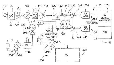
poor,
leading to unacceptable performance in real-life applications.
[00003] The commonly used architecture for radio (wireless) receivers is that
which is referred to as the superheterodyne receiver architecture. This type
of
receiver performs at least one frequency down-conversion of the analog carrier
(RF)
frequency to an intermediate frequency (IF), using a local synthesizer (i.e. a
reference frequency synthesizer/phase locked loop (PLL) circuit) and mixer
circuit to
obtain the baseband signal. Architectures using both a fixed and non-fixed IF
are
known but, disadvantageously, known architectures for the former require the
use of
at least two synthesizer/PLL circuits and those for the latter are not
normally suited
for using sub-sampling and require a high dynamic range in the IF and second
down-conversion, due to channeling and aliasing factors, respectively. These
requirements of known architectures increase the overall power requirements of
the
receiver.
[00004] Accordingly, there is a need for an improved receiver architecture
which provides narrow band selection capability and low power consumption.
1
CA 02643096 2008-08-25
WO 2007/104131 PCT/CA2007/000276
DETAILED DESCRIPTION OF ILLUSTRATED EMBODIMENT
(i) Brief Description of the Drawings
[00005] A better understanding of the invention will be obtained by
considering
the detailed description below, with reference to the following drawings in
which like
references refer to like elements throughout:
[00006] Figure 1 is a schematic block diagram of exemplary receiver circuitry
in
accordance with an embodiment of the invention, and also shows complementary
transmitter local oscillator (Tx LO) circuitry for illustration purposes;
[00007] Figures 2A through 2F collectively depict the RF-to-IF and IF-to-base
band frequency conversions of a receiver configured according to Figure 1;
[00008] Figure 3 is a block diagram illustration of the circuitry which
operates to
pre-tune the Rx LO prior to injection locking with the fractional-N phase
locked loop
PLL);
[00009] Figure 4A is a block diagram illustration of the IF filter Q-tuning
circuitry
for narrow bandpass filtering and Figure 4B is an exemplary circuit for a Q-
tunable IF
filter;
[00010] Figure 5 is a more detailed block diagram illustration of the Rx LO
showing the injection locking circuitry; and,
[00011] Figure 6 is a more detailed block diagram illustration of the receiver
sub-sampling circuitry.
(ii) Description
[00012] Aspects of the claimed receiver architecture provide radio frequency
(RF) receiver circuitry, and a method, for down-converting an RF signal to
base
band. RF-to-IF conversion circuitry, configured for RF-to-IF conversion of the
RF
2
CA 02643096 2008-08-25
WO 2007/104131 PCT/CA2007/000276
signal to an IF signal, comprises mixer circuitry for down-converting the RF
signal to
a band pass IF signal. Local oscillator circuitry is configured for injection
locking and
generating an RF-to-IF mixing signal for input to the mixer circuitry, the
mixing signal
having a frequency which is a first pre-selected harmonic (e.g. 9) of a
reference
frequency. Tunable IF filter circuitry is configured for pre-tuning (e.g. a
center
frequency parameter and/or a Q parameter of) the IF filter to the band of the
band
pass IF signal and, when so tuned, for filtering the band pass IF signal. IF-
to-base
band conversion circuitry, configured for IF-to-base band conversion of the IF
signal,
comprises sub-sampling and down-conversion circuitry operating at a sampling
frequency of a sampling signal input thereto, the sampling frequency being a
second
pre-selected harmonic (e.g. 2) of the reference frequency. Reference frequency
source circuitry (e.g. a synthesizer) is configured for generating a reference
signal of
the reference frequency, wherein the mixing signal and the sampling signal are
derived from the reference signal as a harmonic thereof.
[00013] Selectably operable injection locking pre-tuning circuitry is
configured
for pre-tuning the local oscillator circuitry to an injection locking
frequency sufficiently
within a locking bandwidth of the local oscillator circuitry to enable
injection locking
by the first pre-selected harmonic of the reference signal. The injection
locking pre-
tuning circuitry operates the sub-sampling down-conversion circuitry at
selectable
sampling frequencies determined by digital baseband circuitry for down-
converting
the RF signal wherein the selectable sampling frequencies are selected for
producing those alias bands from which the injection locking frequency is
distinguished on the basis of a measure of energy of the down-converted RF
signal.
An energy detect component is configured for determining that measure of
energy.
The sub-sampling and down-conversion circuitry preferably comprises I and Q
complex signal component sub-samplers and the receiver circuitry may also
include
analog to digital circuitry and digital baseband circuitry comprising a
microcontroller
which selects said reference frequency. The tunable IF filter circuitry
preferably
includes a noise generator configured for generating, and selectably inputting
to the
tunable IF filter circuitry, a white noise signal for use in tuning the
tunable IF filter
circuitry.
3
CA 02643096 2008-08-25
WO 2007/104131 PCT/CA2007/000276
[00014] Figure 1 illustrates an embodiment of the receiver architecture 100
(and for illustrative purposes only also shows, in dotted outline, a possible
transmitter circuitry 220 for advantageously using a complementary transmitter
architecture having a local transmitter oscillator (Tx LO) 205 which is also
injection
locked using a harmonic of the reference oscillator 115). An example of a
product
application of this architecture incorporates the receiver transmitter
circuitry into
portable electronics for which power consumption is a key advantage and which
may
use multiple channels spread through the 2.4 GHz industrial, scientific and
medical
(ISM) radio band, for example.
[00015] Referring to Figure 1, the receiver architecture 100 advantageously
comprises only one a local synthesizer, namely, the reference frequency
synthesizer/phase locked loop (PLL) circuit 115, hereinafter also referred to
in more
general terms as the "reference frequency source". This reference frequency
source
is used for both the RF-to-IF and IF-to-base band conversion processes which,
in
turn, provides for lower power consumption. The illustrated synthesizer/PLL115
is of
the conventional type, to provide a programmable reference frequency output
signal.
Two features of the receiver architecture 100 contribute to enabling this
novel use of
only one reference frequency source.
[00016] One such feature of the receiver 100 is a configuration which uses
injection locking to tune the local receiver oscillator (Rx LO) 105 which is
used for
the first mixing stage (i.e. the RF-to-IF conversion). Advantageously, the RF-
to-IF
mixing signal output from Rx LO 105 is a high-level harmonic of the relatively
low
frequency of the reference frequency source (synthesizer/PLL circuit) 115
which, in
the illustrated example, is the gth harmonic. Also, in this example, it is
seen that a
fractional-N phase locked loop (PLL) is selected for use as the reference
frequency
source.
[00017] The other such feature of the receiver 100 is the use of a pre-tunable
Q-enhanced IF filter 110 with sub-samplers/mixers 130, 140 for the second
4
CA 02643096 2008-08-25
WO 2007/104131 PCT/CA2007/000276
conversion stage (i.e. IF-to-baseband conversion). This enables use of sub-
sampling with a harmonic of the reference frequency, driven by the same
reference
frequency source 115, which is the 2"d harmonic in the illustrated example (it
is to be
recognized by the skilled reader that this reference to a harmonic is intended
to
mean a numerical multiple frequency thereof).
[00018] As a result, the two conversion stages are harmonically related and
driven off the same frequency reference source 115 which, advantageously, can
be
configured as a relatively low frequency source due to the combined usage of
injection locking in the receiver architecture. Moreover, by using a non-fixed
IF
(sometimes referred to as a "walking" IF) with tunable IF bandpass filtering,
the
aliasing obstacle normally presented by sub-sampling is resolved, and allows
the
use of sub-sampling for the second conversion in this architecture. The use of
sub-
sampling is also enabled by the use of the relatively low frequency source 115
as it
then allow for use of a lower harmonic thereof for the sub-sampling. As will
be
immediately recognized by persons skilled in the art, this novel receiver
architecture,
which avoids the conventional usage of two synthesizer circuits for the two
conversions and, in addition, performs the second down-conversion by sub-
sampling, advantageously reduces power consumption.
[00019] Table 1 below provides a set of exemplary frequency values (in MHz)
at various stages of the receiver architecture for each of 16 channels
provided by
the headphone product application, wherein a 5 MHz channel spacing is selected
between RF frequencies and a crystal providing a frequency, of 22.57MHz is
used:
CA 02643096 2008-08-25
WO 2007/104131 PCT/CA2007/000276
Table 1
Channel f f. f f f-
1 2403 115.8072 231.6145 2084.53 318.4699
2 2408 116.0482 232.0964 2088.867 319.1325
3 2313 116.2892 232.5783 2093.205 319.7952
4 2418 116.5301 2330602 2097.542 320.4578
2423 116.7711 233.5422 2101.88 321.1205
6 2428 117.012 234.0241 2106.217 321.7831
7 2433 117.253 234.506 2110.554 322.4458
8 2438 117.494 234.988 2114.892 323.1084
9 2443 117.7349 235.4699 2119.229 323.7711
2448 117.9759 235.9518 2123.566 324.4337
11 2453 118.2169 236.4337 2127.904 325.0964
12 2458 118.4578 236.9157 2132.241 325.759
13 2463 118.6988 237.3976 2136.578 326.4217
14 2468 118.9398 237.8795 2140.916 327.0843
2473 119.1807 238.3614 2145.253 327.747
16 2478 119.4217 238.8434 2149.59 328.4096
[00020] From the foregoing Table 1 it will be seen that the frequencies of
these signals are related according to the following:
fRF =(n '/4)=f~ , wherein n is selected to be 21
41,17 2=fy
fR,i.o 9=fFi.i.
f,,.= 2.75=fs
[00021] The optimal choice of n is dependent on the choice to be made for f,
for any particular application. A higher value of n allows a choice of a lower
value for
fs and, as the reader will recognize, this is desirable to lower the power
consumption
since the PLL and sub-sampler can then run at lower frequencies. In addition,
the
choice of an appropriate value for n depends on the spacing between signal
images
6
CA 02643096 2008-08-25
WO 2007/104131 PCT/CA2007/000276
that can be tolerated for a given circuit configuration, since the higher the
value of n
the closer will be the image signals. Phase noise may also present a factor to
be
considered in respect of a particular design and, thus, play a part in an
optimal
choice of the value of n. For example, ts may be chosen to be sufficiently
high that
the image signals are far enough away from the band pass IF signal that the IF
filter
attenuates them to such a degree as to render them ineffectual. In the
exemplary
embodiment illustrated herein the choice of '/4 in the relationship fRF =(n
'/4)=fs is for
the purpose of simplifying the down conversion process whereby discrete-time,
complex signal components output from the sub-samplers 130 are, in effect,
multiplied by a series of (1,0,-1,0) for the I component and by (0,1,0,-1) for
the Q
component, to produce the corresponding output baseband signal components 142
[00022] The received RF signal 10 is processed by an attenuator 40 for
automated gain control (using a gain control signal 20 generated by the
baseband
digital processing circuitry 165 based on channel energy detection) and fed to
a low
noise amplifier (LNA) 120 loaded with a tank circuit RF filter 45 (i.e. off-
chip). The
overall Q of the RF filter 45 is nominally mid-range (e.g. 30 for the
aforesaid ISM 2.4
GHz band) so as to provide some band selection. The resulting processed RF
signal 122 is then down-converted by means of mixer 125 to convert the signal
from
the RF carrier to an IF (Intermediate Frequency) carrier. Advantageously, this
is
done by means of an injection locked local oscillator circuit (Rx LO) 105
which is
configured for pre-tuning and driven from the aforesaid reference frequency
source
which is, here, a relatively low frequency fractional-N PLL 115 based on a
crystal
oscillator 160. This allows for a relatively high harmonic of the PLL 115 to
lock the
Rx LO 105.
[00023] The current output of mixer 125 is fed into the intermediate frequency
(IF) Q-tuned filter 110 which also has off-chip inductors in the exemplary
embodiment (it being understood that another design, and frequency plan, could
instead be made to use on-chip inductors). For an intermediate frequency of
approximately 320 MHz the IF filter 110 is Q-enhanced to a bandwidth of 5 MHz.
Advantageously, this Q-enhancing allows the use of the sub-sampler 130 by
7
CA 02643096 2008-08-25
WO 2007/104131 PCT/CA2007/000276
providing the anti-aliasing which is necessary in order to use such sub-
sampling. It
also, provides some channel selection. Moreover, the use of this high Q filter
before
a large amount of the receiver gain occurs improves the dynamic range of
receiver
100 and allows lower power consumption in subsequent stages.
[00024] The first-stage down converted signal 112 is fed to an IF amplifier
(IFA)
135 comprised of source followers with gm boosting feedback which drives the
second stage mixer comprising I and Q signal component sub-samplers 130 and
sub-sampling mixers 140. The I, Q signals 132 output from the sub-samplers 130
have a bandpass frequency domain centered at f~/4, where fG is the effective
sampling frequency as shown in Figures 1 and 2. Sub-sampling mixers 140
modulate the signal 132 and convert it to a continuous time low-pass signal
142.
[00025] The following components of the receiver shown in Figures 1-4A will be
well-known to and understood by persons skilled in the art and many variations
and
modifications may be devised for use in a specific application. For example, a
programmable gain amplifier (PGA) 145 may be used to provide a requisite gain
in
the exemplary headphone transceiver application and an analog-to-digital
converter
(ADC) 150 may comprise a 2nd order continuous-time filter and 2-bit quantizer,
but it
will be recognized that because the signal here is low-pass and partially
filtered, the
requirements of linearity and bandwidth on PGA 145 and ADC 150 are relaxed. An
analog control signal 20 for automatic gain control by the attenuator 40 is
produced
by automatic gain control (AGC) digital processing circuitry 155 using channel
energy detection in receiver digital baseband circuitry 165. In addition, a
state
machine (not shown) may react to a saturation signal 153 from ADC 150, to
cause
the receiver gain to be reduced by PGA 145 in response to a control signal 22
produced by the AGC circuitry of the digital baseband circuitry 165 based on
residual out-of-band interference detected at ADC 150 (but is digitally
filtered and
does not form part of the energy detection).
[00026] With reference to the signals shown at circuit locations identified in
Figure 2A, Figures 2B through 2F depict the frequency domain of the signal at
each
8
CA 02643096 2008-08-25
WO 2007/104131 PCT/CA2007/000276
such point whereby these figures collectively illustrate the RF-to-IF and IF-
to-base
band frequency conversions of a receiver configured according to Figure 1.
Figure
2A is largely the same as Figure 1 but, for convenience, doesn't show the
receiver
local oscillator (Rx LO) circuitry 105 and some other components shown in
Figure 1
so that it shows only one-half of the I-Q processing circuitry starting with
the
sub-sampling circuitry. Figure 2B graphically depicts the frequency domain of
the
received RF signal at location (a) of Figure 2A and also shows the RF-to-IF
mixing
signal Rx LO which is output from the local oscillator circuit Rx LO 115.
Figure 2C
graphically depicts the frequency domain of the down-converted IF signal at
location
(b) of Figure 2A. Figures 2D and 2E graphically depict the I and Q signal
components for the IF-to-base band frequency down conversion, the former
depicting the frequency domain of the sub-sampled signal at location (c) (and,
as will
be recognized by persons skilled in the art, in actuality the I and Q signal
components will each be at fs/2 rather than the fs/4 used here for ease of
illustration)
and the latter depicting the frequency domain of the mixer-converted signal at
location (d) of Figure 2A. Figure 2F depicts the down-converted signal at
location
(d) after processing by the analog-to-digital converter (ADC).
[00027] With reference to Figure 1 it will be noted by the reader skilled in
the
art that a transmitter 200 can readily make use of a complementary
architecture to
that of receiver 100. As is done in receiver 100, a transmit local oscillator
(Tx LO)
205 with off-chip inductors can, similarly, be injection lock driven from a
harmonic of
the reference frequency source (PLL) 115. For example, for the transmit mode,
PLL
115 may be adjusted to a slightly different frequency (e.g. -220 MHz) so that
direct
up-conversion is possible using, for example, the 11th harmonic of PLL 115.
The
clock rate of the transmitter baseband is the frequency of crystal oscillator
160 and
the PLL 115 is able to achieve a very low current draw while meeting a
switching
time constraint of 60ps between the transmit (Tx) and receive (Rx)
frequencies.
Then, the other circuit components 220 of transmitter 200 may be arranged in a
standard configuration, well known to those in the art.
9
CA 02643096 2008-08-25
WO 2007/104131 PCT/CA2007/000276
[00028] As highlighted above, the single reference synthesizer architecture of
the receiver 100 avoids the necessity for a second radio frequency (RF) PLL by
making use of injection locking the RX LO 105 which is the subject of U.S.
Patent
No. 6,963,249 issued on 8 November, 2005 and assigned to the same assignee as
this application. In turn, this injection locking is achieved in this
embodiment by
digitally pre-tuning the Rx LO 105 to an injection locking frequency which is
sufficiently within a locking bandwidth of the Rx LO, to enable injection
locking to
occur when the PLL 155 reference signal is input to the Rx LO. The pre-tuning
brings the free-running frequency of the oscillator close enough to the
desired
frequency so that injection locking can be guaranteed. Without this pre-
tuning, it
would not be possible to injection lock Rx LO 105 (or Tx LO 205) given the
process
variation of the oscillator's tank circuit.
[00029] As illustrated by Figure 3, the digital processing capability of the
digital
baseband circuitry 165 is used to determine the center frequency (fc) of the
output of
the Rx LO 105 (and possibly also Tx LO 205 in the complementary transmit
circuit
architecture, but without a repetitive description thereof being provided
hereinafter).
The tuning of the Rx LO 105 is accomplished in the digital domain. To begin,
the
reference frequency signal provided by PLL 115, which is normally input to the
Rx
LO 105, is disabled and instead a secondary path is enabled, as described in
the
following. The pre-tuning is performed by transmitting the output of Rx LO
105, via
this secondary path as illustrated, directly to the sub-sampler 130 and the
receiver
100 determines the center frequency of the output of the Rx LO 105 during this
secondary path-mode. The sub-sampled signal 137 is processed for gain and
converted to digital form (via gain and DAC components 145, 150). The
resultant
digital signal is processed in the digital domain, using a digital
microcontroller in the
receiver baseband circuitry 165, to determine the center frequency (fc) of the
Rx LO
105.
[00030] As persons skilled in the art will understand, a number of different
methods are available for the required determination of f, In the exemplary
embodiment, this is accomplished through the use of an "energy detect"
component
CA 02643096 2008-08-25
WO 2007/104131 PCT/CA2007/000276
(not specifically shown in the drawings) within the receiver digital baseband
circuitry
165 which generates a signal proportional to the energy in the signal band. In
this
discussion, with reference to Figure 3, it is the frequency of the RX LO 105
output to
be determined (tested). Because the digital baseband is of finite bandwidth,
if the
center frequency of the RX LO 105 output being tested is in the channel, this
becomes obvious from the output signal generated by the energy detect
component.
[00031] According to this procedure, the frequency of the PLL 115 is set so
that the sampling frequency used during this secondary path-mode performs a
frequency conversion that would match with a conversion from the desired
frequency of the Rx LO 105, the desired frequency being the targeted injection
locking frequency at which the Rx LO is sufficient pre-tuned for injection
locking and
RF-to-IF down-conversion for the pre-selected RF channel. Then a sweep of the
frequency of the RX LO 105, from maximum down, is performed and at each step,
the energy detect component output signal is considered. The sweep is stopped
when the output of the energy detect component goes above a certain limit and,
at
this point, it is known that the frequency of the RX LO 105 is either at the
injection
locking frequency or, instead, at an alias frequency. Due to the latter
possibility it is
then necessary to determine which is correct, before the tuning is complete.
So, the
PLL 115 is then set to a second sampling frequency, such that the desired
frequency of the RX LO 105 will still fall in-band, but the undesired alias
frequencies
will not fall in-band. From this information it is determined (i.e. as the
logical result of
this) whether or not there has been a verification that the desired frequency
has
been reached; if so, the Rx LO has been pre-tuned to the injection locking
frequency
for that RF channel. If the desired frequency isn't found by this step, the
sweep is
continued from where it left off to find the next peak, and this algorithm is
repeated
until the desired match condition is met.
[00032] For purposes of instruction only, the reader is asked to consider a
scenario for which it is desired to tune the RX LO 105 to receive an RF signal
of
frequency f, equal to 2408 MHz. To implement the process for tuning the RX LO
105 to this desired (target) channel, the microcontroller first sets the
sampling
11
CA 02643096 2008-08-25
WO 2007/104131 PCT/CA2007/000276
frequency to 116 MHz. The RX LO 105 is set to a predetermined maximum
frequency and a sweep of its frequency is instituted until the applicable
threshold
energy is detected by the energy detect component. At this point it is not
known
whether the desired frequency is actually being output by the RX LO 105. Let's
consider for explanatory purposes that, at this point, it is actually
outputting a
frequency for tuning into a channel having an fRF value of (2408 + 116/2) MHz
=
2466 MHz, that is, the first alias band above the desired frequency channel.
Therefore, at this point, it is impossible to tell whether the desired
frequency is being
output by the Rx LO 105. Then, the sampling frequency (fs) is set so that
instead of
a factor of 20.75 (i.e. in the relationship fRF =(nf'/4)=ft, wherein n is
selected to be 21,
such that the factor n+'/4 is 20.75 or 21.25), the other factor of 21.25 is
used. This
means that the sampling frequency is set to 113.3MHz. This frequency will also
find
2408 MHz; however, it will not find 2466 MHz (since 2408 +113.3/2= 2464).
Thus, if
the sampling frequency were to be changed accordingly there would no longer be
any such detection of a peak in the energy at baseband. So, returning to the
process with use of the original sampling frequency, the frequency sweep is
performed and eventually another peak in energy is detected but this time when
the
second sampling frequency is applied a peak energy is still detected at
baseband,
meaning that the Rx LO 105 output is now at the desired frequency to tune to
this
channel.
[00033] Once the Rx LO 105 frequency is determined it is adjusted by fedback
control signals 166 and 168 which are generated, as aforesaid, by the digital
baseband circuitry 165 and converted to analog form by digital-to-analog
converters
172. This pre-tuning feedback process is continuously repeated until the
desired Rx
LO 105 frequency is reached.
[00034] When the Rx LO 105 has been pre-tuned close enough to the desired
oscillation frequency (i.e. to within the LBW) to allow injection locking, the
PLL 115 is
once again enabled and the pre-tuning secondary path is disabled.
[00035] By pre-tuning Rx LO 105 so that its oscillation frequency f, is close
to
the desired frequency, the required locking bandwidth (LBW) for injection
locking to
12
CA 02643096 2008-08-25
WO 2007/104131 PCT/CA2007/000276
be achieved is reduced significantly. A reduction in the LBW reduces the
required
power of the injection locking reference frequency source 115 signal and, in
turn,
this allows use of higher harmonics of a relatively low reference frequency to
be
used for down-conversion. As shown in Figure 1, a low frequency crystal
oscillator
160 with PLL 115 are used to injection lock the RF Rx LO 105 with the xth
harmonic,
in this example x being selected to be 9.
[00036] Figure 5 is a more detailed block diagram illustration of the Rx LO
105
showing the injection locking circuitry. A square wave is output from PLL 115
(thus,
having large harmonic content) and applied to a band pass filter (BPF) 119 to
select
the desired, odd harmonic wherein an odd harmonic is used in the headphone
receiver application because a differential input is applied to the Rx LO 105
(the 9`n
harmonic being used in that application). Once that selected harmonic signal
is
applied to the Rx LO 105, the Rx LO 105 becomes and remains locked to that
harmonic signal. As shown, in the RX LO 105 circuitry the harmonic signal is
then
converted to a current by the injection locking transconductor 126 and fed
directly
into the core 128 of RX LO 105.
[00037] The injection locking bandwidth is typically related to the input
injection
locking power with the latter increasing (in dBm) as the former increases. The
phase noise of the resulting locked LO is a factor of n2 or 201og(n) higher
than the
phase noise of the source signal (i.e. PLL 115), where n is the injection
locking
harmonic used. Persons skilled in the art will be familiar with the known
measures
available to counter this effect, where desired. These include inter alia the
possibility of using an off-chip tank circuit with a high Q inductor for PLL's
115 core
voltage controlled oscillator (VCO) or, to reduce the effect of phase noise on
the
error vector magnitude (EVM) in the receiver (and transmitter), the
possibility of
using a differential detection scheme (it being well known in the art that
differential
detection has the effect of rejecting close in-phase noise from the incoming
signal).
[00038] The filter Q-tuning circuitry which is advantageously used for narrow
bandpass filtering by the IF filter 110 is shown by Figure 4A. Figure 4B
provides an
13
CA 02643096 2008-08-25
WO 2007/104131 PCT/CA2007/000276
exemplary circuit for the Q-tunable IF filter component. As is well known, the
bandpass frequency response of filter 110 is characterized by its filter
parameter Q
and its center frequency f,, and, for additional discussion of directly tuning
a filter the
reader may refer to U.S. Patent No. 6,983,136 issued on 3 January, 2006 and
assigned to the same assignee as this application.
[00039] In the exemplary example described herein, the filter 110 is pre-tuned
according the following process. As a first step the filter 110 is placed in
oscillation
by increasing its Q parameter past the point of oscillation. Then the
frequency f, of
the filter 110 is determined in similar manner to that described above for
determining
the frequency of RxLO 105, until the frequency is within about 2 MHz (i.e.
within
about 1%) of the desired center frequency.
[00040] Then, once the frequency f, of the filter 110 is within that target of
the
desired frequency, the circuit path from the local oscillator Rx LO 105 is
disabled
and, instead, a secondary path from a noise generator 300 is enabled. This
noise
generation path provides to filter 110 a white noise signal having a
substantially flat
power spectral density. The noise signal is then filtered by IF filter 110 to
produce at
the filter output 117 a signal having a power spectral density which is
proportionally
representative of the frequency response of the IF filter 110. The filter
output 117 is
fed directly to the sub-sampler 130 and the sub-sampled signal is then
processed for
gain and converted to digital form (via gain and ADC components 145, 150). The
resultant digital signal is processed in the digital domain, using a digital
microcontroller in the receiver baseband circuitry 165, to determine the
filter
parameters Q and f,
[00041] The digital processing circuitry 165 produces digital control signals
112
for adjustment of the Q and fc of the filter 110. These are converted to
analog
control signals 116, 118 using digital-to-analog converters (DACs) 114. As
shown
by Figure 4B, the filter 110 is equipped to have analog filter adjustment
inputs a and
b that directly adjust a respective filter element for each characterizing
parameter.
14
CA 02643096 2008-08-25
WO 2007/104131 PCT/CA2007/000276
[00042] In the exemplary example described herein the filter 110 parameters f,
and Q are determined as follows. A digital filter (not shown) having a narrow
bandwidth is used to more finely resolve the frequency response of the IF
filter 110.
This is done by setting the PLL 115 such that the desired center frequency of
the IF
filter 110 is converted and then the power is calculated by the digital
filter, thereby
providing the power at that center frequency. Then the PLL 115 frequency is
changed (the required change in fPLL being derived per the foregoing frequency
equations) such that f,+5 MHz is captured by filter 110 and the power is
calculated.
Then a third such reading is performing using f,-5 MHz so that three different
power
points are known (i.e f,+5MHz, f, and f,-5MHz). Then the PLL 115 frequency is
adjusted, and the foregoing three point measurement steps repeated, until the
calculated powers at the edges i.e. at each of f,-5MHz and f,+5MHz, become
equal
since this indicates that the filter 110 is centered between those two points.
After
this, the value of the parameter Q for filter 110 is calculated using the
ratio of the
powers at f, and one of f,-5MHz and f,+5MHz (as is well-known, there is a 1-to-
1
correspondence between Q and this ratio).
[00043] It will be recognized by the skilled reader that there are different
methods for determining the filter 110 parameters fc and Q which might be
adaptable
to a particular application depending on required speed, accuracy and power
requirements. Examples of other such methods include those described in the
assignee's aforementioned U.S. Patent No. 6,983,136; and, performing an FFT of
the sampled data (i.e. removing the narrow band desired signal and any other
interfering signals, smoothing the amplified noise if necessary and finding
the peak
of the resultant frequency response). Other alternatives are also known in the
art
and, depending on any particular speed, accuracy and/or power requirements,
one
such other method may be chosen as appropriate for a given application.
[00044] Referring to Figure 6, a more detailed block diagram illustration of
the
receiver sub-sampling circuitry 130 is provided. The IF signal is offset from
a
harmonic of the sampling frequency fs by a factor of fs/4 causing images to
appear at
offsets of f,/2. Baseband conversion is then easily facilitated with alternate
inversion
CA 02643096 2008-08-25
WO 2007/104131 PCT/CA2007/000276
of the signal by mixer 140. As will be readily understood by persons skilled
in the
art, the notation (1, -1) to each mixer 140 in Figures 1 and 2 signifies the
conversion
to DC. Wideband noise from the IFA 135 and sub-sampling mixer 140 are also
then
mixed down, increasing the noise density. IFA 135 is a source follower,
designed
with low enough output impedance to drive the sampling capacitors. The noise
generated by IFA 135 and sub-sampler 130 is essentially set by the size of the
sampling capacitors 138. Larger capacitors will decrease the kT/C noise and a
larger gm in IFA 135 will decrease the wideband noise from IFA 135. To
maintain
the sampler bandwidth, the switches are sized properly, putting an effective
limit on
how large the capacitors can be made.
[00045] The closest image due to the sub-sampling is at an f,/2 offset, or
approximately 60 MHz offset for the particular example described herein. For
the
first and last few channels, this image lands in-band and has the most effect,
while
the center channels are not significantly affected.
[00046] With the foregoing exemplary embodiment of the invention having
been disclosed, it will be apparent to those skilled in the art that various
changes
and modifications can be made which will achieve the advantages of the
invention
all of which are intended to fall within the scope of the invention as defined
by the
claims that follow.
16