Note: Descriptions are shown in the official language in which they were submitted.
CA 02643175 2008-08-20
WO 2007/098151 PCT/US2007/004353
ADJUSTABLE INDUSTRIAL ANTENNA MOUNT
BACKGROUND
The present discussion relates to
industrial process control monitoring devices. More
particularly, the present discussion relates to field
devices configured to communicate wirelessly with
remote devices in process control systems that are
adapted for use in harsh environmental conditions.
Electronic field devices (such as process
transmitters) can be used to monitor the operation of
industrial processes such as those in oil refineries,
chemical processing plants, paper processing plants,
biotechnology plants, pharmaceutical plants, food and
beverage plants, and the like. Process transmitters
for monitoring an industrial process may be used to
measure one or more phenomena that are related to or
capable of impacting the process. Some phenomena that
may be measured in industrial processes include
pressure, flow rate, fluid or material level in a tank,
temperature, and vibration. Additionally, such field
devices may include electronics capable of performing
analysis of measured data related to one or more
phenomena, diagnostic electronics, or other process
monitoring electronic devices, or even electronic,
hydraulic, or pneumatic actuator devices used for
industrial process control.
Field devices can also include circuitry
for communicating over a process control loop with
other monitoring or control devices such as, for
example, other installed field devices, hand held
tools, or equipment that may be remotely located, for
CA 02643175 2008-08-20
WO 2007/098151 PCT/US2007/004353
-2-
example, in a process control room. Data transmitted
over the process control loop can be transmitted in
either an analog or a digital format. Analog field
devices are often connected to other devices via two-
wire process control current loops. For example, a
number of field devices can be connected to a process
control room via a single two-wire control loop.
In addition or alternatively, field devices
can have wireless communication technologies
incorporated to facilitate communication with other
remotely located monitoring and control devices.
Wireless communication technologies provide the
advantage of simplifying field device implementation
because field devices that do not rely on wired
communication need not have any wires provided to
them. For certain types of wireless communication,
an antenna is attached to the field device and is in
electrical communication with wireless communication
circuitry located with the field device to boost the
transmitted signals.
Field devices, including process
transmitters, can be routinely located in relatively
harsh environments. Such environments may be
potentially deleterious to, for example, electrical
components and/or electrical connectors of the field
device, including connections for two wire
communication loops and/or antennas. For example,
process transmitters can potentially be installed in
locations where they are exposed to liquids, dust and
CA 02643175 2008-08-20
WO 2007/098151 PCT/US2007/004353
-3-
humidity and various industrial contaminants. Some of
these field devices may be exposed to potentially
corrosive process liquids, such as acid or base
solutions, that are a part of the particular industrial
process. Such liquids may drip, splash, or be sprayed
onto the field. In addition, field devices may be
exposed to other materials, such as -cleaning agents.
In addition, field devices may be exposed to
electromagnetic waves that can potentially interfere
with the operation of electrical components within
the field device, including the process transmitter
and wireless communication devices. Furthermore,
field devices can be located in external
environments, where they can be exposed to, for
example, temperature extremes, vibration,
precipitation, ultra-violet light, and wind.
In view of the harsh environments in which
field devices are installed and in view of the need to
provide a wireless signal to remote devices in such
environments, there is an ongoing need in the art for
industrial process transmitter housing configurations.
Such housing configurations require improved robustness
with respect to harsh environmental conditions,
including exposure to dust, liquids, humidity, and
electromagnetic energy. In addition, such devices
require an ability to communicate properly with other
wireless devices.
CA 02643175 2008-08-20
WO 2007/098151 PCT/US2007/004353
-4-
SUMMARY
The discussion is directed towards devices
and methods for providing wireless communication in
an industrial process control system. More
particularly, the discussion is directed toward
systems and methods for employing a rotatable antenna
mount with such a device.
In one embodiment, a field. device is
discussed. The'f ield device includes a housing having
an outer surface, an inner surface surrounding a main
cavity, and an aperture extending from the main cavity
to the outer surface. An electrical component is
located within the main cavity of the housing. An
antenna is in electrical communication with the
component. The field device further includes a
rotatable mount that is attached to the housing. The
rotatable mount has a channel that extends from a first
end to a second end. A cable is electrically connected
to the electrical component and the antenna. The cable
extends through at least a portion of the channel.
In another embodiment, an antenna mount for
a field hardened industrial device is discussed. The
antenna mount includes a first portion having an outer
surface *and an inner surface defining a first cavity
that extends from a first end to an aperture at the
outer surface of a second end. The antenna mount
further includes a second portion having an outer
surface and an inner surface defining a second cavity
that extends from a first end to an aperture at the
CA 02643175 2012-04-25
- 5 -
outer surface of a second and. The fixet and second
portion, are attached to eaCkh rather along a generally
planar attachment surface at their first ends. The
attacbrnent aiurface is not perpendicular to the any of
the outer surface at the second ends of the first end
second Portion .
In yet e-uather embodiment, a method of
attaching an antenua to a field hardened i udttstr lal
device -is discussed. The matbod iualudee atteAhiug e.
rotatable naum to a housing of the field hardened
industrial device. The method further includes
providing an electrical coxanectio between an antenna
to on, electrical component located within the housing.
The mount is rotated relative to the housing to adjust
the p00itiou'of the ants.
According to an aspect Of the present
invention, there is provided a field device,
comprising:
a housing having an outer surface, an inner
surface surrounding a main cavity, and an aperture
extending from the main cavity to the outer
surface;
an electrical component located within the main
cavity of the housing;
an antenna in electrical communication with the
electrical component;
a rotatable mount attached to the housing and
having a channel extending from a first end to a
second end;
a cable electrically connected to the electrical
component and the antenna; and
wherein the cable extends through at least a
portion of the channel;
wherein at least a portion of the rotatable mount
comprises a polymer material, wherein the rotatable
mount further comprises, a generally hollow sleeve
formed from a conductive material, and the sleeve
is positioned within and attached to at least a
portion to the channel.
CA 02643175 2012-04-25
-5a-
According to another aspect of the present
invention, there is provided a field device,
comprising:
a housing having an outer surface, an inner
surface surrounding a main cavity, and an aperture
extending from the main cavity to the outer
surface;
an electrical component located within the main
cavity of the housing;
an antenna in electrical communication with the
electrical component;
a rotatable mount attached to the housing and
having a channel extending from a first end to a
second end;
IS a cable electrically connected to the electrical
component and the antenna, wherein the cable
extends through at least a portion of the channel;
and
a ferrite element coupled to the rotatable mount
and positioned to receive and surround a portion of
the cable.
According to a further aspect of the
present invention, there is provided a field
device, comprising:
a housing having an outer surface, an inner
surface surrounding a main cavity, and an aperture
extending from the main cavity to the outer
surface;
an electrical component located within the main
cavity of the housing;
an antenna in electrical communication with the
electrical component;
a rotatable mount attached to the housing and
having a channel extending from a first end to a
second end; and
a cable electrically connected to the electrical
component and the antenna;
wherein the cable extends through at least a
portion of the channel;
CA 02643175 2012-04-25
- 5b -
wherein the rotatable mount has a first portion
and second portion, the first portion is configured
to be inserted into the aperture, the first portion
is positioned at an angle with respect to the
second portion, the first portion is positioned at
about a 45-degree angle with respect to the second
portion.
According to a further aspect of the
present invention, there is provided a field
l0 device, comprising:
a housing having an outer surface, an inner
surface surrounding a main cavity, and an aperture
extending from the main cavity to the outer
surface;
an electrical component located within the main
cavity of the housing;
an antenna in electrical communication with the
electrical component;
a rotatable mount attached to the housing and
having a channel extending from a first end to a
second end;
a cable electrically connected to the electrical
component and the antenna; and
wherein the cable extends through at least a
portion of the channel, wherein the rotatable mount
has a first portion and second portion wherein the
first portion is configured to be inserted into the
aperture, and wherein further
the first portion is provided with a first and a
second groove into which are placed first and
second sealing elements and wherein a notch is
defined in a portion of the housing that defines
the aperture such that when the first portion is
positioned within the aperture the sealing element
engages both the groove and the notch so as to seal
the aperture and provide enough retention force to
hold the mount in a chosen orientation.
According to a further aspect of the
present invention, there is provided a method of
CA 02643175 2012-04-25
- 5c -
attaching an antenna to a field hardened industrial
device, comprising :
attaching a rotatable mount to a housing of the
field hardened industrial device;
providing an electrical connection between an
antenna to an electrical component located within
the housing; and
rotating the mount relative to the housing to
adjust the position of the antenna, the method
further comprising:
providing first and a second grooves on a
first portion of the rotatable mount and placing
first and second sealing elements into the first
and a second grooves,
providing a notch in a portion of the
housing that defines the aperture into which the
first portion of the rotatable mount is attached,
and
positioning the first portion within the
aperture so that the sealing element engages both
the groove and the notch so as to seal the
aperture and provide enough retention force to
hold the mount in a chosen orientation.
According to a further aspect of the present invention
there is provided a field device, comprising:
a housing having an outer surface, an inner
surface surrounding a main cavity, and an aperture
extending from the main cavity to the outer surface;
an electrical component located within the main
cavity of the housing;
an antenna in electrical communication with the
electrical component;
a rotatable mount attached to the housing and
having an internal channel; and
a cable electrically connected to the electrical
component and the antenna,
wherein the cable extends through at least a
portion of the internal channel,
CA 02643175 2012-04-25
5d
wherein the rotatable mount comprises a first
portion and a second portion, the first portion being
configured to be at least partially inserted into the
aperture,
wherein the first portion has a first portion
inner surface defining a first segment of the internal
channel, the first segment extending from a first end
of the first portion to an opening at an outer surface
of a second end of the first portion, and
wherein the second portion has a second portion
inner surface defining a second segment of the
internal channel in communication with the first
segment, the second segment extending from a first end
of the second portion to an opening at an outer
1S Surface of a second end of the second portion, and
wherein the. first and second portions are
attached to each other along a generally planar
attachment surface at their first ends and wherein the
attachment surface is not perpendicular to any of the
outer surfaces at the second ends of the first and
second portions.
S=2V u CRIPTf+O[z OF TM IMA"XIM
?IQ _ ., 1 3.s a block diagram of a pr'ooess
enviranmanb illustrating a field hardened iMuetrial
device with which an adJueatable lmdustriaal antenna
mount in acaoxdencs with the present disclosure in
pea?t.itvlaxly useful.
FIG. 2 is a block diagraaa of the field
device Qf FICA. i, illustrating an eleotridal circuit
coupled to an antenna at a rotatable ant acucirdixug
to one illustrative embodiment.
VZO, 3 is a scheraatic diagram of the field
device of FIG_ 3., illuetxratin e= industrial antenna
mount according to oqe i:luatxative embodiuent.
CA 02643175 2008-08-20
WO 2007/098151 PCT/US2007/004353
-6-
FIG. 4 is a perspective view of the
industrial antenna mount of FIG. 3.
FIG. 5 is a cross sectional view of the
field device of FIG. 3 taken along line 5-5.
FIG. 6 is an enlarged portion of the cross
sectional view of FIG. 4.
FIG.- 7 is cross sectional view of an
industrial antenna mount including a sleeve extending
into a portion of the mount according to one
illustrative embodiment.
FIG. 8 is a cross sectional view of an
industrial antenna mount including a sleeve extending
from one end of the antenna mount to the other
according to one illustrative embodiment.
FIG. 9 is a cross sectional view of an
industrial antenna mount having a sleeve extending
through the mount with a notch formed therein
according to one illustrative embodiment.
FIG. 10 is a cross sectional view of an
industrial antenna mount having an embedded ferrite
element formed therein according to one illustrative
embodiment.
FIG. 11A is a cross sectional view of an
industrial antenna mount having an attachment for a
base of an antenna integrated into the mount
according to one illustrative embodiment.
FIG. 11B is a cross sectional view of an
industrial antenna mount having an attachment for a
base of an antenna with a conductive portion of the
CA 02643175 2008-08-20
WO 2007/098151 PCT/US2007/004353
-7-
attachment in electrical communication with the mount
according to one illustrative embodiment.
FIG. 11C is an enlarged portion of the
industrial antenna mount of FIG. 11B detailing a
connection between the attachment and mount according
to one illustrative embodiment.
FIG. 12 is a perspective view of the field
device of FIG. 3 with a radome attached to the
antenna mount in one orientation according to one
illustrative embodiment.
FIG. 13 is a perspective view of the field
device of FIG.12 with the antenna mount in another
orientation.
FIG. 14 is a perspective view of an antenna
mount having a generally straight configuration
according to one illustrative embodiment.
FIG. 15 is a flowchart depicting a method
of positioning an antenna on a wireless field device
according to one illustrative embodiment.
While the above-identified illustrations
set forth embodiments of the present invention, other
embodiments are also contemplated, some of which are
noted in the discussion. In all cases, this
disclosure presents the illustrated embodiments by
way of representation and not limitation.
DETAILED DESCRIPTION
The present discussion is directed to a
field hardened industrial device, such as a process
transmitter. As used herein, the phrase "field
CA 02643175 2008-08-20
WO 2007/098151 PCT/US2007/004353
-8-
hardened industrial device" or, alternatively, "field
device" refers to a device with a housing for use in
harsh environmental conditions including outdoor
applications. The housing of the field hardened
industrial device of the current discussion is sealed
to protect the contents against environmental
contamination. In addition, the housing is designed
to be resistant to electromagnetic and/or radio
frequency interference that might otherwise be induced
or conducted onto electrical devices or circuitry
contained within it.
Field hardened industrial devices of the
type to which the current discussion is directed are
capable of wireless communication with a remote
device. A remote device can be any device outside of
the particular field hardened industrial device in
question. For example, the remote device can be a
handheld device, another field hardened industrial
device in the. same environment such as the same
process room or general area, or a device located
outside of the same environment such as, for example,
a device in a control room.
FIG. 1 is a block diagram that illustrates
a process environment 10 in which a field hardened
industrial device 12 is illustratively employed.
Process environment 10 can be one of any number of
industrial environments, including, for example,
manufacturing, refining, or many other applications
in which it is advantageous to monitor one or more
CA 02643175 2008-08-20
WO 2007/098151 PCT/US2007/004353
-9-
phenomena and/or control a particular process. The
field hardened industrial device .12, in one
illustrative embodiment, is capable of sensing one or
more process phenomena 14 to which it is exposed and
providing a signal indicative' of a status of the
given process phenomenon. Examples of the types of
phenomena 14 to which the- field hardened industrial
device 12 may be exposed include temperature,
pressure, fluid flow, pH levels, etc. Alternatively,
field hardened industrial device 12 may be exposed to
and be configured to measure a plurality of phenomena
14. Alternately, or in addition, the field hardened
industrial device 12 may include an actuation device,
which can control a process or a portion of a
process.
Field hardened industrial device 12
illustratively includes a housing 20 in which a
transducer (26 shown in FIG 2) is enclosed. The
transducer 26 is capable of providing a signal
indicative of phenomenon 14 to which it is exposed.
Field hardened industrial device 12 also
illustratively includes an antenna 18, which is
coupled to housing 20. The antenna 18 is in
electrical communication with the remote electrical
device 16 and can send and receive signals
transmitted between the electrical component 16 of
field hardened industrial device 12 and a remote
electrical device 16.
CA 02643175 2008-08-20
WO 2007/098151 PCT/US2007/004353
-10-
FIG. 2 is a functional block diagram
illustrating field device 12 in more detail according
to one illustrative embodiment. Field device 12
includes a power module 22 for supplying power to the
other components within the f ield device 12. Power
module 22 can utilize any acceptable technology to
provide appropriate electrical signal levels to
various devices within the field device 12. For
example, power module 22 can employ known thermopile
devices to generate electricity from disparate
temperatures using the Peltier Effect, including, but
not limited to thermoelectric diodes; solid state
thermogenerators; and semiconductor thermoelectric
generators. Alternatively, power module 22 can
include a solar cell. Other types of power modules
can be used such as, for example, batteries. For
example, in lieu of an onboard power module 22, an
external power supply (not shown) can provide a power
signal to the field device 12.
Field device 12 also illustratively
includes a controller 24, and a wireless
communication device 28 located within housing 20
along with transducer 26. Power module 22
illustratively provides power to each of the
controller 24, transducer 26 and wireless
communication device 28. As discussed above,
transducer 26 is, in one embodiment, configured to
measure a phenomenon to which it is exposed.
Alternatively, transducer 26 can generate an output
CA 02643175 2008-08-20
WO 2007/098151 PCT/US2007/004353
-11-
signal to control an external component (not shown)
Controller 24 is in communication with the transducer
26 to send and/or receive signals to or from the
transducer 26. Controller 24 also provides signals
to the wireless communication device 28, which in
turn is capable of communicating information with
remote devices.
Wireless communication device 28 can
communicate process-related information as well as
device-related information. Depending upon the
application, wireless communication device 28 may be
adapted to communicate in accordance with any
suitable wireless communication protocol including,
but not limited to: wireless networking technologies
(such as IEEE 802.11b wireless access points and
wireless networking devices built by Linksys of
Irvine, California), cellular or digital networking
technologies (such as Microburst by Aeris
Communications Inc. of San Jose, California) ultra
wide band, free space optics, Global System for
Mobile Communications (GSM), General Packet Radio
Service (GPRS), Code Division Multiple Access (CDMA),
spread spectrum technology, infrared communications
techniques, SMS (Short Messaging Service/text
messaging), or any other suitable wireless
technology. Further, known data collision technology
can be employed such that multiple units can coexist
within wireless operating rage of one another. Such
collision prevention can include using a number of
CA 02643175 2008-08-20
WO 2007/098151 PCT/US2007/004353
-12-
different radio-frequency channels and/or spread
spectrum techniques.
Wireless communication device 28 can also
include transducers for a plurality of wireless
communication methods. For example,. primary wireless
communication could be performed using relatively
long distance communication methods, such as GSM or
GPRS, while a secondary, or additional, communication
method could be provided for technicians or operators
near the unit, using for example, IEEE 802.11b or
Bluetooth.
Some wireless communications modules may
include circuitry that can interact with the Global
Positioning System (GPS). GPS can be advantageously
employed in field device 12 for mobile devices to
allow finding the individual field device 12 in a
remote location. However, location sensing based
upon other techniques can be used as well.
Field device 12 illustratively includes
capability for wireless communication. Additionally,
field device 12 can, but need not, include the
capability to communicate via a wired communication
protocol with other remote devices such as other
field devices, displays, and other monitoring or
control devices. Wired communication can be
advantageous if the field device 12 is required to
communicate with other devices that do not have
wireless communication capability. To that end,
field device 12 can be equipped to communicate, for
CA 02643175 2008-08-20
WO 2007/098151 PCT/US2007/004353
-13-
example, with devices over a two-wire process loop
(not shown) Examples of process control loops that
might be incorporated include analog 4-20 mA
communication, hybrid protocols which include both
analog and digital communication such as the Highway
Addressable Remote Transducer (HART ) standard, as
well as all-digital protocols such as the FOUNDATION'
Fieldbus standard-
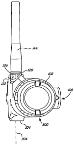
Fig 3 illustrates a portion of a field
hardened industrial device 100 of the type described
above according to one illustrative embodiment.
Field device 100 includes a housing 102, which
provides an enclosure for components such as the
electrical devices discussed above. Housing 102, in
one embodiment, is formed from a high strength
material such as stainless steel, aluminum, or other
acceptable material. The housing 102 can be attached
to one or more sensing devices (not shown), which are
intended to be exposed to, for example, liquids,
gases or other materials for the purpose of measuring
a particular phenomenon. Each sensing device
illustratively provides a signal to electrical
components within the housing 102. Such electrical
components are illustratively adapted to determine a
measurement based upon signals provided by the
sensing device.
Alternatively or in addition, an actuation
device (not shown) can be attached to the housing 102
and be in electrical communication with electrical
CA 02643175 2012-04-25
-14-
cciiponents located within the housing 102. The
e3.eatrical con one.nts within the hmming 2.03 can
illuetrar ' ra1y provide a signal, to control the
actuation device, Which in turn can control an aspect
of a part:LOv- ar process. It should be appreciated
that a single device attached the housing 102 can
prorwide both a sensing and an actuation function.
The representative housing illustrated In
FIG. 3 includes three ports 104, lob, and 1001 to
which the sensing and/or actuation device may be
attached. Housing 102 can thus be i3lt stratively
connected to the sensing and/or actuation device, in a
number of different orientations. Ports 104, 3.06 and
1D6 are shown and detailed in part to show the
orient-ti on. of the housing 102 in different FXGv.
that are a part of the current "atsmion. Any
configuration of ports can be employed in housing 102,
and this dieoussicn is not intended to limit the
arrangement of ports in the housing 7.02 of field
device 100 in any way. -Xn addition, the field device
100 bas a rotatable antenna mount 110 attached to the
housing 102. Further, it should be appreciated that
although FIG. 3 illustrates a housing 102 that is
configured to be attached to one or more sexxsi.ng
and/or aotuation devices, housing 102 can include a
sensing 'and/or actuation device located within it.
CA 02643175 2008-08-20
WO 2007/098151 PCT/US2007/004353
-15-
FIG. 4 shows a perspective view of the
rotatable mount 110 according to one-- illustrative
embodiment. The rotatable mount 110. includes a body
112, which, in one illustrative embodiment, is formed
from a polymeric material, although other suitable
materials may be used including conductive materials
such as, for example, aluminum. The body 112
illustratively includes an upper portion 111 and a
lower portion 113. The upper portion. 111 and the
lower portion 113 are, in one illustrative embodiment
connected or attached to each other along an angled
attachment surface 115. While the upper portion 111
and the lower portion 113 are described as being
connected or attached to each other, it should be
appreciated that the upper and lower portions 111 and
113 can be formed from a single, integral piece of
material. The upper and lower portions 111 and 113
are illustratively connected to each other along one
of each of their ends. The.. angled surface 115 is
angled with respect to the general orientation of
each of the upper and lower portions Ill and 113. In
one illustrative embodiment, the upper and lower
portions 111 and 113 extend from the angled surface
115 at about a 45-degree angle with respect to each
other.
The body 112 includes a channel 120 that
extends from an aperture 122 on the upper portion 111
to an aperture 118 on the lower portion 113. Because
the upper portion 111 and the lower portion 113 are
CA 02643175 2008-08-20
WO 2007/098151 PCT/US2007/004353
-16-
shown as being angled with respect to each other,
channel 120 is illustratively an angular path from
the aperture 118 to the aperture 122. Rotatable
mount 110 illustratively includes a pair of grooves
130 and 132 that extend around, a perimeter of the
lower portion 113 of the body 112. Grooves 130 and
132 are each configured to accept a sealing device,
which will be discussed in more detail below.
Rotatable mount 110 also illustratively
includes a threaded portion 124 on its upper portion
111. The threaded portion 124 is configured to be
engaged with a cover such as a radome (not shown in
FIG. 4), which is discussed in more detail below. A
groove 128 is formed into the upper portion Ill at an
end of the threaded portion 124 that is closer to the
lower portion 113 of the body 112. A sealing element
(not shown in FIG. 4) such as an o-ring can be placed
onto the body 112 so that it is captured in the
gropve, 128. Thus, when a cover is attached to the
rotatable mount 110, the sealing element located in
groove 128 can provide a seal to prevent moisture,
dirt or other materials from entering into the
channel 120 of the rotatable mount 110.
FIGs. 5 and 6 illustrate a cross sectional
view of the field device 100 shown in FIG. 3.
Rotatable mount 110 is shown positioned within an
aperture 114 in FIG. 5 (and in an exploded view in
FIG. 6) that extends from an outer surface 103 of
housing 102 through housing 102 to provide access to
CA 02643175 2012-04-25
-17-
a main cavity 117. Main cavity 117 is defined by an
inner surface 105 of housing 102- The electrical
cocaponents discussed above with respect to FxG- 3,
Including the power "module 33, controller 24,
transducer- 26, and wireless punication device 2
are illustratively positioned within the main cavity
13.7. An antenna can be atKaohed or positioned
adjacent to the rotatable mount 110 (hot shown In
FYC3s. 5 and 6) . Coainadtion can be made between the
antenna and the electrical cowonents such an by, for
example, a coaxial Cable that extends into the
rotatable mount 110 from the rain cavity 13.7 loot
shown in FIGs. 5-6) . The coaxial cable is connected
to the antenna either within or external . to the
rotatable ntCXt7.nt iio. other connecting arreugetnents
between the electrical components within main cavity
3.3.7 and the antenna can be emplmleed.
Furauaat to one embodiment, a notch 116 is
formd into a portign of the housing 3.03 that defines
the aperture 114. The notch x16 illustratively
extends around a perimeter Of they aperture 13.4. The
rotatable mo=t 110 is i.17.uWtrative1y shown with
sealing elements 3.34 and 136 positioned. in grooves
130 and 132, respectively. In one illustrative
elements 3.34 and 136 are o-
eml~odin-esat, the eaa].issg
ri.zIgo, although other devices can bg used.- For
exz~le. a ataining ring or clip can be inserted
CA 02643175 2008-08-20
WO 2007/098151 PCT/US2007/004353
-18-
into groove 130 in lieu of, or in addition to,
sealing element 134. The rotatable mount 110 is
positioned within the aperture 114 so that the
sealing element 134 (or the retaining ring or clip)
engages both the groove 130 and the notch 116.
Alternatively, or in addition, a set screw or one or
more detents (not shown) can be employed to hold the
mount 110 in a desired orientation.
The engagement of sealing element 134 with
the groove 130 and the notch 116 provides a retaining
force that keeps the rotatable mount 110 positioned
within the aperture 114. In addition, the rotatable
mount 110 is capable of rotating within the aperture
114 about axis 126. Because the channel 120 is
angled, rotating the rotatable mount 110 about axis
will change the orientation of an antenna that is
attached to the rotatable mount 110. This allows the
antenna to be positioned as desired. Further still,
the engagement of the sealing element 134, the groove
130, and the notch 116 provide enough retention force
to prevent the mount 110 from rotating unless an
outside force is applied to the mount 110. The
sealing element 136 provides protection from foreign
matter entering the main cavity 117 of the housing
102 through the aperture 114 while allowing rotation
of the mount 110.
As discussed above, the body 112 of mount
110 is illustratively made of a polymeric material.
Thus, the channel 120 is illustratively surrounded by
CA 02643175 2008-08-20
WO 2007/098151 PCT/US2007/004353
-19-
such material. FIGs. 7-9 illustrate alternative
embodiments of mount 110. Mount 140 includes a body
112 with a sleeve 142 that is illustratively inserted
into, but not beyond a portion the channel 120 in the
lower portion 113 of body 112. The sleeve 142 is
illustratively made of a different material than that
of body 112. As one illustrative example, the sleeve
is made of aluminum, although a number of different
materials may be used. Sleeve 142 is illustratively
molded into the body 112, although alternatively, the
sleeve 142 can be inserted into the body 112 after
the body 112 has been molded. Sleeve 142, in one
embodiment, includes a tab 144, which extends into
the body 112 to provide a retention force to ensure
that the sleeve 142 is retained within the body 110.
The sleeve 142 provides additional strength to the
mount 140_ While sleeve 142 is shown as extending
into the lower portion 113, it can extend into the
body 112 any distance. As an example, mount 150
includes a sleeve 152 that extends through the entire
channel 120 from aperture 118 to aperture 122. The
mount 150 is formed from a material such as aluminum
that provides strength to resist fatigue or impact-
related failure that may be caused by a force applied
to an antenna mounted to the mount 150.
Furthermore, while the sleeve 142, when
inserted or positioned within the rotatable mount 110
is shown as defining the channel 120, alternatively a
sleeve or other reinforcing elements can be molded
CA 02643175 2008-08-20
WO 2007/098151 PCT/US2007/004353
-20-
into or attached to the rotatable mount in other
locations. For example, structural reinforcements
can be contained within the polymeric material that
forms the rotatable mount. In another alternative,
the reinforcement elements can define part or the
entire outer surface 103 of body 112.
Referring to FIG. 8, mount 160 includes a
sleeve 162 that also extends through the channel 120
from the aperture 118 to the aperture 122. However,
sleeve 162 also has a notch 164 formed into it.
Sleeve 162, as discussed above, can be formed from a
material such as aluminum. The sleeve 142 is
illustratively formed from a straight tube. The
process of bending a straight tube to such an angle
can be difficult. By forming. a relief such as notch
164, the sleeve 162 is advantageously more easily
manufactured-
FIG. 10 illustrates a mount 170 according
to yet another embodiment. Mount 170 includes a
ferrite element 172 that is molded into the body 112
of mount 170. Ferrite element 172 is illustratively
a cylindrically shaped member with an aperture 174
formed through its center. The ferrite element 172
advantageously provides filtering of electrical
interference that may be conducted or inducted onto,
for example, a cable that extends into the channel
120. The ferrite element 172 can be of any suitable
size- In addition, the ferrite element 172 can
alternatively be included with other mounts such as,
CA 02643175 2008-08-20
WO 2007/098151 PCT/US2007/004353
-21-
for example, mount 140. While the ferrite element is
shown as being molded into the body 102 of mount 140,
the ferrite element can be inserted into the channel
120 and secured therein through the use of a variety
of different structures or methods.
FIG. 11A illustrates a mount 180 according
to yet another embodiment. Mount 180 includes a body
112. As discussed above, body 112 can be formed from
a number of different materials. In this particular
embodiment, body 112 is illustratively formed from a
non-conductive material. Mount 180 includes a
circuit board or circuit card assembly 184 that is
positioned within the aperture 122 of the body 112.
The circuit board 184 has a connector 186 attached to
it for engaging an antenna. In one illustrative
embodiment, the connector 186 is a subminiature
version A (SMA) connector.
The circuit board 184 illustratively
includes a layer of conductive material 188, which is
formed on the circuit board 184. The conductive
material 188 can be located on either or both major
surfaces of the circuit board 184 as is shown in FIG.
11A. The circuit board 184 can include filtering
circuitry such as filtering component 185 to provide
noise reduction on the signal received from or
provided to the antenna. A cable 182 having a
connecting device 187 is illustratively attached to a
connector 189 to provide a connection between the
CA 02643175 2008-08-20
WO 2007/098151 PCT/US2007/004353
-22-
antenna and electronics located within the main
cavity (117 shown in FIG. 5).
In one illustrative embodiment, a cable 183
is attached to the conductive layer 188 and includes
a connector 181, which is configured to be attached
to the housing 102. Cable 183 can be of any length
so as to be mounted to the housing 102 at an
appropriate location. Cable 183 is illustrated as
being broken to indicate that the length of cable 183
can be variable to allow the cable 183 to be attached
to the housing 102 at any location. The layer of
conductive material 188 is thereby in electrical
communication with the housing 102 when the cable 183
is attached to the housing 102. The filtering
components 185 are illustratively positioned between
the conductive layer 188 and any conductor attached
to the antenna. The signal from the antenna is thus
filtered to reduce electrical noise that may be
induced onto the antenna.
FIGs. 11B-C illustrate a mount 190
according to another illustrative embodiment. Mount
190 includes a body 112 that is formed from a
conductive material. Mount 190 further includes a
circuit board or circuit card assembly 192 that is
positioned within the aperture 122 of the body 112.
Circuit card assembly 192 has a conductive layer 194
of material that extends around an edge 196 of the
circuit card assembly 192. The circuit card assembly
192 is illustratively attached to the body 112 of
CA 02643175 2008-08-20
WO 2007/098151 PCT/US2007/004353
-23--
mount 190 such as by a solder joint 198 formed
between the conductive layer 194 and the body 112.
The solder joint 198 provides a connection between
the. body 112 and the circuit card assembly 192. In
addition, the solder joint 198 provides a conductive
path between the conductive layer 192 and the body
112.
As discussed above, the body 112 in the
illustrative embodiment is formed from*a conductive
material. Therefore, when the body 112 is attached
to the housing 102, the conductive layer 194 is in
electrical communication with the housing 102.
Filtering component 185, which is positioned between
the connector 186 and the conductive layer 192
provides filtering to reduce electrical noise that
may be induced onto the antenna.
FIGs. 12 and 13 illustrate a field device
300 in accordance with one illustrative embodiment.
The field device 300 includes a housing 102 with a
rotatable antenna mount 110 attached to the housing
102. A radome 302 is attached to the mount 110.
Radome 302 is, in one illustrative embodiment,
attached to the mount 110 by engaging the threads
(124, shown in FIG. 4) located on the mount 110. The
rotatable mount 110 is shown in FIG. 12 as being
oriented so that the radome 302 extends along an axis
304 that runs through the apertures 104 and 106. In
FIG. 13, the rotatable mount is oriented so that the
radome 302 extends generally normal to the axis 304.
CA 02643175 2008-08-20
WO 2007/098151 PCT/US2007/004353
-24-
It=is to be understood that the mount 110 is not
limited to these two positions, but can be positioned
in any number of positions as needed to ensure that
the antenna is properly oriented depending on the
orientation of the installed field device 300. The
radome 302 provides environmental protection for the
antenna (not shown) located within the radome 302. A
sealing element 129 is positioned around groove 128
(shown in FIG. 5) to provide additional sealing
protection.
FIG. 14 illustrates an antenna mount 200
according 'to another illustrative embodiment.
Antenna mount 200 is shown in cross section and is,
in one illustrative embodiment, generally symmetrical
about the axis on which the cross section was taken-
Antenna mount 200 is attached .to a housing 202 of a
field device 204. Antenna mount 200 includes a body
206, with a channel 208 that extends from a first end
210 to a second end 212 of the body 206. Antenna
mount 200 is illustratively made of the same types of
materials as previously discussed embodiments.' In
addition, although not shown in FIG. 14, mount 200
can alternatively include a sleeve of the type shown
in FIGs. 7-9, a ferrite element of the type shown in
FIG. 10, and/or a connector of the type shown in 'FIG.
11.
The antenna mount 200 extends into an
aperture 218 formed into the housing 202. The mount
includes a body 206 that illustratively has a channel
CA 02643175 2008-08-20
WO 2007/098151 PCT/US2007/004353
-25-
208 extending from a first aperture"210 to a second
aperture 212. The channel 208 is configured to
accept a cable or other device to provide a
connection between electrical components (not shown
in FIG. 14) and an antenna (also not shown in FIG.
14) that is connected to antenna mount 200. The
antenna mount 200 includes a pair of grooves 214 and
220. The groove 214 is configured to accept a
sealing element 216, which in one illustrative
embodiment is an o-ring, to engage both the portion
of the mount 200 that defines the groove 214 and the
portion of the housing that defines a perimeter of
the aperture 218. In addition, a collar 222 is
configured to engage a lower portion-226 of the body
206. The collar 222 engages the lower portion 226
and the housing 202 to provide a retaining force to
maintain the antenna mount 200 in engagement with the
housing 202. Body 206 also includes threads 224
located. on an upper portion 228 of the body 206. A
radome (not shown in FIG 14) or other device can be
attached to the antenna mount 200 at the threads 224
to provide environmental protection for the antenna
and any components located within a main cavity 230
in the housing 202.
The antenna mount 200, as illustrated in
FIG. 14, is capable of being rotated with respect to
the housing 202. However, the channel 208, unlike
the channel 120 in previous embodiments is generally
linear in its shape from the first aperture 210 to
CA 02643175 2008-08-20
WO 2007/098151 PCT/US2007/004353
-26-
the second aperture 212 and is generally aligned with
an axis about which the antenna mount is capable of
rotating. Thus, rotating the antenna mount 200
generally does not change the orientation of the
antenna with respect to the housing 202.
FIG. 15 is a flowchart illustrating a
method 400 of use for field device 300 (shown in
FIGs. 12-13) having an antenna mount 110. In step
402, the antenna mount 110 is attached to the housing
102. An antenna (not shown in FIGs. 12-13) is
connected with electronics located within the housing
102, as shown by step 404. The antenna can be
covered with a cover such as the radome 302. The
antenna can be attached to the rotating mount,
positioned within the rotatable mount 110, or
positioned externally with respect to the rotatable
mount 110. For example, the antenna can be attached
to the radome. The antenna is then placed in a
desired. orientation by rotating the rotatable mount
110 as is shown in block 406. The rotatable mount
110 can be rotated into any of a number of positions.
In one illustrative embodiment, the rotatable mount
110 has an infinite number of positions over the
range of its acceptable rotation. The range of
rotation can be unlimited or alternatively may be
limited to a defined total angle of rotation.
The embodiments discussed above provide
important advantages. The mounts discussed above
provide an easy way to rotate an antenna into a
CA 02643175 2012-04-25
proper' orieutwtlc .. as is determined by the
orientaticx- in which a particular field device is
metalled. The mounts also pxovift sealing for the
internal cavity of the field device. rn addition,
ewu= of the embodiments provide reinforcement sleeves
to provide additional strength as needed- Antennae
can be positioned within the cover or directly
attached to the mount.
Although the present discussion has been
focused on Illustrative embodiments, workers skilled
in the art will recognize that changes may be made in
f=m =d detail.