Note: Descriptions are shown in the official language in which they were submitted.
CA 02643644 2008-08-27
WO 2007/103265 PCT/US2007/005520
ELECTRO-OPTICAL ELEMENT INCLUDING METALLIC FILMS AND
METHODS FOR APPLYING THE SAME
CROSS REFERENCE TO RELATED APPLICATIONS
[ooo1l This application claims the benefit of U.S. Provisional Application No.
60/779,369, filed March 3, 2006, entitled IMPROVED COATINGS AND REARVIEW
ELEMENTS
INCORPORATING THE COATINGS, and U.S. Provisional Application No. 60/810,921,
filed
June 5, 2006, entitled ELECTROCHROMIC REARVIEW MIRROR ASSEMBLY INCORPORATING A
DISPLAY/SIGNAL LIGHT, both of which are hereby incorporated herein by
reference in their
entirety, and is a continuation-in-part of U.S. Patent Application No.
10/863,638, filed
June 8, 2004, entitled REARVIEW MIRROR ELEMENT HAVING A CIRCUIT MOUNTED To THE
REAR SURFACE OF THE ELEMENT.
BACKGROUND OF THE INVENTION
[00021 This invention relates to electrochromic elements as utilized within
rearview mirror
assemblies for motor vehicles, as well as within window assemblies, and more
particularly, to improved electrochromic elements for use within such
assemblies. More
particularly, the present invention relates to electrochromic elements that
include
conductive layers deposited at atmospheric pressure without compromising
associated
bulk conductivity values.
[0003] Heretofore, various rearview mirrors for motor vehicles have been
proposed which
change from the full reflectance mode (day) to the partial reflectance mode(s)
(night) for
glare-protection purposes from light emanating from the headlights of vehicles
approaching from the rear. Similarly, variable transmittance light filters
have been
proposed for use in architectural windows, skylights, within windows,
sunroofs, and
rearview mirrors for automobiles, as well as for windows or other vehicles
such as aircraft
windows. Among such devices are those wherein the transmittance is varied by
thermochromic, photochromic, or electro-optic means (e.g., liquid crystal,
dipolar
suspension, electrophoretic, electrochromic, etc.) and where the variable
transmittance
characteristic affects electromagnetic radiation that is at least partly in
the visible spectrum
(wavelengths from about 3800A to about 7800 A). Devices of reversibly variable
transmittance to electromagnetic radiation have been proposed as the variable
transmittance element in variable transmittance light-filters, variable
reflectance mirrors,
and display devices, which employ such light-filters or mirrors in conveying
information.
-1-
CA 02643644 2008-08-27
WO 2007/103265 PCT/US2007/005520
[00041 Devices of reversibly variable transmittance to electromagnetic
radiation, wherein
the transmittance is altered by electrochromic means, are described, for
example, by
Chang, "Electrochromic and Electrochemichromic Materials and Phenomena," in
Non-
emissive Electrooptic Displays, A. Kmetz and K. von Willisen, eds. Plenum
Press, New
York, NY 1976, pp. 155-196 (1976) and in various parts of Electrochromism,
P.M.S.
Monk, R.J. Mortimer, D.R. Rosseinsky, VCH Publishers, Inc., New York, New York
(1995). Numerous electrochromic devices are known in the art. See, e.g.,
Manos, U.S.
Patent No. 3,451,741; Bredfeldt et al., U.S. Patent No. 4,090,358; Clecak et
al., U.S.
Patent No. 4,139,276; Kissa et al., U.S. Patent No. 3,453,038; Rogers, U.S.
Patent Nos.
3,652,149, 3,774,988 and 3,873,185; and Jones et al., U.S. Patent Nos.
3,282,157,
3,282,158, 3,282,160 and 3,283,656. In addition to these devices, there are
commercially
available electrochromic devices and associated circuitry, such as those
disclosed in U.S.
Patent No. 4,902,108, entitled "SINGLE-COMPARTMENT, SELF-ERASING,
SOLUTION-PHASE ELECTROCHROMIC DEVICES SOLUTIONS FOR USE
THEREIN, AND USES THEREOF," issued February 20, 1990, to H.J. Byker; Canadian
Patent No. 1,300,945, entitled "AUTOMATIC REARVIEW MIRROR SYSTEM FOR
AUTOMOTIVE VEHICLES," issued May 19, 1992, to J. H. Bechtel et al.; U.S.
Patent
No. 5,128,799, entitled "VARIABLE REFLECTANCE MOTOR VEHICLE MIRROR,"
issued July 7, 1992, to H.J. Byker; U.S. Patent No. 5,202,787, entitled
"ELECTRO-OPTIC
DEVICE," issued April 13, 1993, to H.J. Byker et al.; U.S. Patent No.
5,204,778, entitled
"CONTROL SYSTEM FOR AUTOMATIC REARVIEW MIRRORS," issued Apri120,
1993, to J.H. Bechtel; U.S. Patent No. 5,278,693, entitled "TINTED SOLUTION-
PHASE
ELECTROCHROMIC MIRRORS," issued January 11, 1994, to D.A. Theiste et al.; U.S.
Patent No. 5,280,380, entitled "UV-STABILIZED COMPOSITIONS AND METHODS,"
issued January 18, 1994, to H.J. Byker; U.S. Patent No. 5,282,077, entitled
"VARIABLE
REFLECTANCE MIRROR," issued January 25, 1994, to H.J. Byker; U.S. Patent No.
5,294,376, entitled "BIPYRIDINIUM SALT SOLUTIONS," issued March 15, 1994, to
H.J. Byker; U.S. Patent No. 5,336,448, entitled "ELECTROCHROMIC DEVICES WITH
BIPYRIDINIUM SALT SOLUTIONS," issued August 9, 1994, to H.J. Byker; U.S.
Patent
No. 5,434,407, entitled "AUTOMATIC REARVIEW MIRROR INCORPORATING
LIGHT PIPE," issued January 18, 1995, to F.T. Bauer et al.; U.S. Patent No.
5,448,397,
entitled "OUTSIDE AUTOMATIC REARVIEW MIRROR FOR AUTOMOTIVE
-2-
CA 02643644 2008-08-27
WO 2007/103265 PCT/US2007/005520
VEHICLES," issued September 5, 1995, to W.L. Tonar; and U.S. Patent No.
5,451,822,
entitled "ELECTRONIC CONTROL SYSTEM," issued September 19, 1995, to J.H.
Bechtel et al. Each of these patents is commonly assigned with the present
invention and
the disclosures of each, including the references contained therein, are
hereby incorporated
herein in their entirety by reference. Such electrochromic devices may be
utilized in a
fully integrated inside/outside rearview mirror system or as separate inside
or outside
rearview mirror systems, and/or variable transmittance windows.
[00051 Fig. 1 shows the cross-section of a typical electrochromic mirror
device 10, having
a front planar substrate 12 and a rear planar substrate 16, and of which the
general layout is
known. A transparent conductive coating 14 is provided on the rear surface of
the front
substrate 12, and another transparent conductive coating 18 is provided on the
front
surface of rear substrate 16. A reflector 20, typically comprising a silver
metal layer 20a
covered by a protective copper metal layer 20b, and one or more layers of
protective paint
20c, is disposed on the rear surface of the rear substrate 16. For clarity of
description of
such a structure, the front surface 12a of the front substrate 12 is sometimes
referred to as
the first surface, and the inside (or rear) surface 12b of the front substrate
12 is sometimes
referred to as the second surface, the inside surface 16a of the rear
substrate 16 is
sometimes referred to as the third surface, and the back surface 16b of the
rear substrate 16
is sometimes referred to as the fourth surface. In the illustrated example,
the front substrate
further includes an edge surface 12c, while the rear substrate includes an
edge surface 16c.
The front and rear substrates 12,16 are held in a parallel and spaced-apart
relationship by
seal 22, thereby creating a chamber 26. The electrochromic medium 24 is
contained in
space or chamber 26. An electrochromic medium 24 is in direct contact with
transparent
electrode layers 14 and 18, through which passes electromagnetic radiation
whose intensity
is reversibly modulated in the device by a variable voltage or potential
applied to electrode
layers 14 and 18 through clip contacts and an electronic circuit (not shown).
[00061 The electrochromic medium 24 placed in chamber 26 may include surface-
confined, electrode position-type or solution-phase-type electrochromic
materials and
combinations thereof. In an all solution-phase medium, the electrochemical
properties of
the solvent, optional inert electrolyte, anodic materials, cathodic materials,
and any other
components that might be present in the solution are preferably such that no
significant
electrochemical or other changes occur at a potential difference which
oxidizes anodic
-3-
CA 02643644 2008-08-27
WO 2007/103265 PCT/US2007/005520
material and reduces the cathodic material other than the electrochemical
oxidation of the
anodic material, electrochemical reduction of the cathodic material, and the
self-erasing
reaction between the oxidized form of the anodic material and the reduced form
of the
cathodic material.
100071 In most cases, when there is no electrical potential difference between
transparent
conductors 14 and 18, the electrochromic medium 24 in chamber 26 is
essentially colorless
or nearly colorless, and incoming light (la) enters through the front
substrate 12, passes
through the transparent coating 14, the electrochromic medium 24 in chamber
26, the
transparent coating 18, the rear substrate 16, and reflects off the layer 20a
and travels back
through the device and out the front substrate 12. Typically, the magnitude of
the reflected
image (IR) with no electrical potential difference is about 45 percent to
about 85 percent of
the incident light intensity (Io). The exact value depends on many variables
outlined
below, such as, for example, absorption by the various components, the
residual reflection
(I'R) from the front face of the front substrate, as well as secondary
reflections from the
interfaces between the front substrate 12 and the front transparent electrode
14, the front
transparent electrode 14 and the electrochromic medium 24, the electrochromic
medium
24 and the second transparent electrode 18, and the second transparent
electrode 18 and
the rear substrate 16. These reflections are well known in the art and are due
to the
difference in refractive indices between one material and another as the light
crosses the
interface between the two. If the front substrate and the back element are not
parallel, then
the residual reflectance (I'R) or other secondary reflections will not
superimpose with the
reflected image (IR) from mirror surface 20a, and a double image will appear
(where an
observer would see what appears to be double (or triple) the number of objects
actually
present in the reflected image).
100081 There are minimum requirements for the magnitude of the reflected image
depending on whether the electrochromic mirrors are placed on the inside or
the outside of
the vehicle. For example, according to current requirements from most
automobile
manufacturers, inside mirrors preferably have a high end reflectivity of at
least 70 percent,
and outside mirrors must have a high end reflectivity of at least 35 percent.
100091 The electrode layers 14 and 18 are connected to electronic circuitry
which is
effective to electrically energize the electrochromic medium, such that when a
potential is
applied across the conductors 14 and 18, the electrochromic medium in chamber
26
-4-
CA 02643644 2008-08-27
WO 2007/103265 PCT/US2007/005520
darkens, such that incident light (Io) is attenuated as the light passes
toward the reflector
20a and as it passes back through after being reflected. By adjusting the
potential
difference between the transparent electrodes, such a device can function as a
"gray-scale"
device, with continuously variable transmittance over a wide range. For
solution-phase
electrochromic systems, when the potential between the electrodes is removed
or returned
to zero, the device spontaneously returns to the same, zero-potential,
equilibrium color and
transmittance as the device had before the potential was applied. Other
electrochromic
materials are available for making electrochromic devices. For example, the
electrochromic medium may include electrochromic materials that are solid
metal oxides,
redox active polymers, and hybrid combinations of solution-phase and solid
metal oxides
or redox active polymers; however, the above-described solution-phase design
is typical of
most of the electrochromic devices presently in use.
(0010] Even before a fourth surface reflector electrochromic mirror such as
that show in
Fig. 1, was cornmercially available, various groups researching electrochromic
devices
had discussed moving the reflector from the fourth surface to the third
surface. Such a
design has advantages in that it should, theoretically, be easier to
manufacture because
there are fewer layers to build into a device, i.e., the third surface
transparent electrode is
not necessary when there is a third surface reflector/electrode. Although this
concept was
described as early as 1966, no group had commercial success because of the
exacting
criteria demanded from a workable auto-dimming mirror incorporating a third
surface
reflector. U.S. Patent No. 3,280,701, entitled "OPTICALLY VARIABLE ONE-WAY
MIRROR," issued October 25, 1966, to J. F. Donnelly et al. has one of the
earliest
discussions of a third surface reflector for a system using a pH-induced color
change to
attenuate light.
100111 U.S. Patent No. 5,066,112, entitled "PERIMETER COATED, ELECTRO-OPTIC
MIRROR," issued November 19, 1991, to N. R. Lynam et al., teaches an electro-
optic
mirror with a conductive coating applied to the perimeter of the front and
rear glass
elements for concealing the seal. Although a third surface reflector is
discussed therein,
the materials listed as being useful as a third surface reflector suffer from
the deficiencies
of not having sufficient reflectivity for use as an inside mirror, and/or not
being stable
when in contact with a solution-phase electrochromic medium containing at
least one
solution-phase electrochromic material.
-5-
CA 02643644 2008-08-27
WO 2007/103265 PCT/US2007/005520
[0012] Others have broached the topic of a reflector/electrode disposed in the
middle of an
all solid state-type device. For example, U.S. Patent Nos. 4,762,401,
4,973,141, and
5,069,535 to Baucke et al. teach an electrochromic mirror having the following
structure:
a glass element, a transparent indium-tin-oxide electrode, a tungsten oxide
electrochromic
layer, a solid ion conducting layer, a single layer hydrogen iorrpermeable
reflector, a solid
ion conducting layer, a hydrogen ion storage layer, a catalytic layer, a rear
metallic layer,
and a back element (representing the conventional third and fourth surface).
The reflector
is not deposited on the third surface and is not directly in contact with
electrochromic
materials, certainly not at least one solution-phase electrochromic material
and associated
medium. Consequently, it is desirable to provide an improved high reflectivity
electrochromic rearview mirror having a third surface reflector/electrode in
contact with a
solution-phase electrochromic medium containing at least one electrochromic
material.
Electrochromic windows that have been proposed, typically include an
electrochromic cell
similar to that shown in Fig. 1, but without layer 20a, 20b and 20c.
100131 Whether deposited on the first, second, third, fourth or edge surfaces
of the
substrates, metal containing films or layers that are conductive, reflective,
or both are
significantly useful in the construction of electrochromic electro-optic
devices as well as
the integrated electrochromic devices packaged therewith. Generally, the
versatility and
utility of a metal film or multiple layers of metal films increases: as the
conductivity
increases; as the adhesive properties increase; as the intricacy of the
pattern of the layer
increases; as the reflectivity increases while maintaining a color neutral
reflection; as the
chemical and electrochemical stability increases; and, as the ease of
application increases.
100141 Various attempts have been made to provide an electrochromic element
with
conductive layers on the surfaces of the substrates associated with an
electrochromic
element as discussed above. One such method includes utilizing metal particle
load resins
such as epoxy resins loaded with silver flake. However, the conductivity of
such systems
is limited by the sheer number of particle to particle connections that must
be made in
order to conduct current. Each particle to particle connection adds electrical
resistance,
thereby limiting the usefulness of metal particle loaded resins. Currently, it
is not possible
to obtain mirror-quality specular light reflection from such films since the
random
orientation of the relatively large metal particles promotes diffuse
reflection. In order to
avoid these limitations, it is desirable to deposit metal films that more
closely approach
-6-
CA 02643644 2008-08-27
WO 2007/103265 PCT/US2007/005520
bulk metal properties. Metal films that more closely approach bulk metal
properties for
conduction and reflection adhere well to applicable substrates, are chemically
and electro-
chemically durable, and can be deposited using vacuum processes such as
sputtering or
evaporation. However, the equipment for vacuum-based processes is expensive to
purchase, operate, and maintain. It is further difficult to deposit pattern
films using
vacuum-based processes. One method of patterning vacuum-applied metal films
requires
that the metal be applied through a mask during deposition. Such masks can be
expensive
to machine and difficult to maintain. Another method of patternin.g a vacuum-
applied
metal film requires that the metal be removed after deposition by additional
processing
steps such as laser ablation or chemical etching. Aside from increasing the
complexity of
the overall manufacturing process, the aforementioned sputtering or
evaporation processes
are also not efficient in the use of metal or metal precursors. Specifically,
a significant
amount of metal is deposited on the masking and surrounding structure rather
than on the
desired device during the vacuum processing, the reclamation of the which is
costly and
time consuming.
[0015] It is therefore desirable to produce metal films within electrochromic
or other
electro-optic devices under near atmospheric conditions, and specifically
atmospheric
pressure, and that provide adequate conductive, adhesive and reflective
properties, while
maintaining a color neutral reflection, adequate chemical and electro-chemical
stability,
and simultaneously allowing for an increase in application control.
SUMMARY OF THE INVENTION
[0016] One aspect of the present invention includes a method of manufacturing
an
electrochromic element that comprises providing a first substrate having a
first surface, a
second surface opposite the first surface, and a first edge surface, providing
a second
substrate having a third surface facing the second surface, a fourth surface
opposite the
third surface, and a second edge surface, and providing an electrochromic
medium
between the first and second substrates wherein the electrochromic medium has
a light
transmittance that is variable upon the application of an electric field
thereto. The method
further includes applying a conductive layer on at least a portion of at least
a select one of
the first surface, the second surface, the first edge surface, the third
surface, the fourth
surface and the second edge surface, wherein applying the conductive layer is
accomplished at substantially atmospheric pressure and includes applying at
least a select
-7-
CA 02643644 2008-08-27
WO 2007/103265 PCT/US2007/005520
one of inetallic particles, an inorganal metallic, a metallo-organic, and
combinations
thereof, and wherein the conductive layer has a bulk conductivity of greater
than or equal
to 150 S2-cm.
[0017] Another aspect of the present inventive method for manufacturing an
electrochromic element comprises providing a first substrate having a first
surface, a
second surface opposite the first surface, and a first edge surface, providing
a second
substrate having a third surface facing the second surface, a fourth surface
opposite the
third surface, and a second edge surface, and providing an electrochromic
medium
between the first and second substrates wherein the electrochromic medium has
a light
transmittance that is variable upon the application of an electric field
thereto. The method
further includes inkjet printing a conductive layer on at least a portion of
at least a select
one of the first surface, the second surface, the first edge surface, the
third surface, the
fourth surface and the second edge surface.
[00i8] Yet another aspect of the present inventive method includes providing a
first
substrate having a first surface, a second surface opposite the first surface,
and a first edge
surface, providing a second substrate having a third surface facing the second
surface, a
fourth surface opposite the third surface, and a second edge surface, and
providing an
electrochromic medium between the first and second substrates wherein the
electrochromic medium has a light transmittance that is variable upon the
application of an
electric field thereto. The method fiirther includes ultrasonic spraying a
conductive layer
on at least a portion of at least a select one of the first surface, the
second surface, the first
edge surface, the third surface, the fourth surface and the second edge
surface.
[0019] Still yet another aspect of the present inventive method comprises
providing a first
substrate having a first surface, a second surface opposite the first surface,
and a first edge
surface, providing a second substrate having a third surface facing the second
surface, a
fourth surface opposite the third surface, and a second edge surface, and
providing an
electrochromic medium between the first and second substrates wherein the
electrochromic medium has a light transmittance that is variable upon the
application of an
electric field thereto. The method further includes applying a conductive
layer on at least a
portion of at least a select one of the first surface, the second surface, the
first edge surface,
the third surface, the fourth surface and the second edge surface, wherein
applying of the
conductive layer includes at least a select one of auger pumping and jet
pumping.
-8-
CA 02643644 2008-08-27
WO 2007/103265 PCT/US2007/005520
[0020) Another aspect of the present inventive method for manufacturing an
electrochromic element comprises providing a first substrate having a first
surface, a
second surface opposite the first surface, and a first edge surface, providing
a second
substrate having a third surface facing the second surface, a fourth surface
opposite the
third surface, and a second edge surface, and providing an electrochromic
medium
between the first and second substrates wherein the electrochromic medium has
a light
transmittance that is variable upon the application of an electric field
thereto. The method
further includes applying a conductive layer on at least a portion of at least
a select one of
the first surface, the second surface, the first edge surface, the third
surface, the fourth
surface and the second edge surface, wherein applying of the conductive layer
includes at
least a select one of combustion chemical vapor deposition, flame spray
deposition, and
laser sintering. =
[00211 These and other features, advantages, and objects of the present
invention will be
further understood and appreciated by those skilled in the art by reference to
the following
specification, claims, and appended drawings.
BRIEF DESCRIPTION OF THE DRAWINGS
[0022] In the drawings:
[0023] Fig. 1 is an enlarged cross-sectional view of a prior art
electrochromic mirror
assembly incorporating a fourth surface reflector;
[0024] Fig. 2 is a front elevational view schematically illustrating an
inside/outside
electrochromatic rearview mirror system for motor vehicles;
[00251 Fig. 3 is an enlarged cross-sectional view of an electrochromic mirror
incorporating
a third surface reflector/electrode taken along the line III-III, Fig. 2;
[0026] Fig. 4 is a flow chart illustrating the sequence of the present
inventive method;
[00271 Fig. 5 is a schematic cross-sectional view of a substrate and a bulk
metal coating
with a larger crystalyte structure;
[00281 Fig. 6 is a schematic cross-sectional view of a substrate and a bulk
metal coating
with a small crystalyte structure; and
[0029] Fig. 7 is a graph of a wavelength versus reflectance for Example No. 7.
DETAILED DESCRIPTION OF THE PREFERRED EMBODIMENTS
[0030] For purposes of description herein, the terms "upper," "lower,"
"right," "left,"
"rear>""front>""vertical>""horizontal>" and derivatives thereof shall relate
to the invention
-9-
CA 02643644 2008-08-27
WO 2007/103265 PCT/US2007/005520
as oriented in Fig. 2. However, it is to be understood that the invention may
assume
various alternative orientations and step sequences, except where expressly
specified to the
contrary. It is also to be understood that the specific devices and processes
illustrated in the
attached drawings, and described in the following specification are exemplary
embodiments of the inventive concepts defined in the appended claims. Hence,
specific
dimensions and other physical characteristics relating to the embodiments
disclosed herein
are not to be considered as limiting, unless the claims expressly state
otherwise.
100311 Fig. 2 shows a front elevational view schematically illustrating an
inside mirror
assembly 110 and two outside rearview mirror assemblies 111a and 111b for the
driver-
side and passenger-side, respectively, all of which are adapted to be
installed on a motor
vehicle in a conventional manner and where the mirrors face the rear of the
vehicle and
can be viewed by the driver of the vehicle to provide a rearward view. While
mirror
assemblies in general are utilized herein to describe the present invention,
it is noted that
this invention is equally applicable to the construction of electrochromic
windows. The
inside mirror assembly 110 and the outside rearview mirror assemblies l l la,
111b may
incorporate light-sensing electronic circuitry of the type illustrated and
described in the
above-referenced Canadian Patent No. 1,300,945, U.S. Patent No. 5,204,778, or
U.S.
Patent No. 5,451,822, and other circuits capable of sensing glare and ambient
light and
supplying a drive voltage to the electrochromic element. In the illustrated
example,
electrical circuitry 150 is connected to and allows control of the potential
to be applied
across the reflector/electrode 120 and transparent electrode 128, such that
electrochromic
medium 126 will darken and thereby attenuate various amounts of light
traveling
therethrough and then vary the reflectance of the mirror containing the
electrochromic
medium 126. The mirror assemblies 110, 111 a, 111b are similar in that like
numbers
identify components of the inside and outside mirrors. These components may be
slightly
different in configuration, but function in substantially the same manner and
obtain
substantially the same results as similarly numbered components. For example,
the shape
of the front glass element of the inside mirror 110 is generally longer and
narrower than
the outside mirrors 111a, 111b. There are also some different performance
standards
placed on the inside mirror 110 compared with the outside mirrors 111 a, 111
b. For
example, the inside mirror 110 generally, when fully cleared, should have a
reflectance
value of about 70 percent to about 85 percent or higher, whereas the outside
mirrors often
-10-
CA 02643644 2008-08-27
WO 2007/103265 PCT/US2007/005520
have a reflectance of about 50 percent to about 65 percent. Also, in the
United States (as
supplied by the automobile manufacturers), the passenger-side mirror 111b
typically has a
spherically bent or convex shape, whereas the driver-side mirror 111 a and the
inside
mirror 110 presently must be flat. In Europe, the driver-side mirror 111 a is
commonly flat
or aspheric, whereas the passenger-side mirror 11 lb has a convex shape. In
Japan, both of
the outside mirrors 111a, 111b have a convex shape. The following description
is
generally applicable to all mirror assemblies of the present invention, while
the general
concepts are equally applicable to the construction of electrochromic windows.
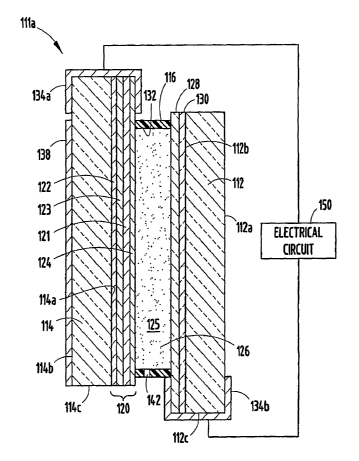
[00321 Fig. 3 shows a cross-sectional view of the mirror assembly l l la
having a front
transparent substrate 112 having a front surface 1 12a and a rear surface 1
12b, and a rear
substrate space 114 having a front surface 1 14a and a rear surface 114b. For
clarity of
description of such a structure, the following designations will be used
hereinafter. The
front surface 112a of the front substrate will be referred to as the first
surface i 12a, and the
back surface 112b of the front substrate as the second surface 112b. The front
surface 114a
of the rear substrate will be referred to as the third surface 114a, and the
back surface 114b
of the rear substrate as the fourth surface 114b. The front substrate 112
further includes an
edge surface 11 2e, while the rear substrate 114 further incli.ides an edge
surface 114c. A
chamber 125 is defined by a layer of transparent conductor 128 (carried on the
second
surface 112b), a reflector/electrode 120 (disposed on the third surface 114a),
and an inner
circumferential wall 132 of a sealing member 116. An electrochromic medium 126
is
contained within the chamber 125.
[0033] As broadly used and described herein, the reference to an electrode or
layer as
being "carried" on or applied to a surface of an element, refers to both
electrodes or layers
that are disposed directly on the surface of an element or disposed on another
coating,
layer or layers that are disposed directly on the surface of the element.
Further, it is noted
that the mirror assembly l l la is described for explanatory purposes only,
and that the
specific components and elements may be rearranged therein, such as the
configuration
illustrated in Fig. 1, and those configurations known for electrochromic
windows.
100341 The front transparent substrate 112 may be any material which is
transparent and
has sufficient strength to be able to operate in the conditions, e.g., varying
temperatures
and pressures, commonly found in the automotive environment. The front
substrate 112
may comprise any type of borosilicate glass, soda lime glass, float glass, or
any other
-11-
CA 02643644 2008-08-27
WO 2007/103265 PCT/US2007/005520
material, such as, for example, a polymer or plastic, that is transparent in
the visible region
of the electromagnetic spectrum. The front substrate 112 is preferably a sheet
of glass. The
rear substrate 114 must meet the operational conditions outlined above, except
that it does
not need to be transparent in all applications, and therefore may comprise
polymers,
metals, glass, ceramics, and preferably is a sheet of glass.
[0035] The coatings of the third surface 1 14a are sealably bonded to the
coatings on the
second surface 112b in a spaced-apart and parallel relationship by the seal
member 116
disposed near the outer perimeter of both the second surface 112b and the
third surface
114a. The seal member 116 may be any material that is capable of adhesively
bonding the
coatings on the second surface 112b to the coatings on the third surface 1 14a
to seal the
perimeter such that the electrochromic material 126 does not leak from within
the chamber
125. Optionally, the layer of transparent conductive coating 128 and the layer
of
reflector/electrode 120 may be removed over a portion where the seal member
116 is
disposed (not the entire portion, otherwise the drive potential could not be
applied to the
two coatings). In such a case, the seal member 116 must bond well to glass.
100361 The performance requirements for the perimeter seal member 116 used in
an
electrochromic device are similar to those for a perimeter seal used in a
liquid crystal
device (LCD), which are well known in the art. The seal 116 must have good
adhesion to
glass, metals and metal oxides; must have low permeabilities for oxygen,
moisture vapor,
and other detrimental vapors and indium; and must not interact with or poison
the
electrochromic or liquid crystal material it is meant to contain and protect.
The perimeter
seal 116 can be applied by means commonly used in the LCD industry, such as by
silk
screening or dispensing. Totally hermetic seals, such as those made with glass
frit or solder
glass, can be used, but the high temperatures involved in processing (usually
near 450 C)
this type of seal can cause numerous problems, such as glass substrate
warpage, changes in
the properties of transparent conductive electrode, and oxidation or
degradation of the
reflector. Because of their lower processing temperatures, thermoplastic,
thermosetting or
UV curing organic sealing resins are preferred. Such organic resin sealing
systems for
LCDs are described in U.S. Patent Nos. 4,297,401, 4,418,102, 4,695,490,
5,596,023, and
5,596,024. Because of their excellent adhesion to glass, low oxygen
permeability and good
solvent resistance, epoxy-based organic sealing resins are preferred. These
epoxy resin
seals may be UV curing, such as described in U.S. Patent No. 4,297,401, or
thermally
-12-
CA 02643644 2008-08-27
WO 2007/103265 PCT/US2007/005520
curing, such as with mixtures of liquid epoxy resin with liquid polyamide
resin or
dicyandiamide, or they can be homopolymerized. The epoxy resin may contain
fillers or
thickeners to reduce flow and shrinkage such as fumed silica, silica, mica,
clay, calcium
carbonate, alumina, etc., and/or pigments to add color. Fillers pretreated
with hydrophobic
or silane surface treatments are preferred. Cured resin crosslink density can
be controlled
by use of mixtures of mono-functional, di-functional, and m.ulti-functional
epoxy resins
and curing agents. Additives such as silanes or titanates can be used to
improve the seal's
hydrolytic stability, and spacers such as glass beads or rods can be used to
control final
seal thickness and substrate spacing. Suitable epoxy resins for use in a
perimeter seal
member 116 include, but are not limited to: "EPON RESIN" 813, 825, 826, 828,
830, 834,
862, 1001F, 1002F, 2012, DPS-155, 164, 1031, 1074, 58005, 58006, 58034, 58901,
871,
872, and DPL-862 available from Shell Chemical Co., Houston, Texas; "ARALITE"
GY
6010, GY 6020, CY 9579, GT 7071, XU 248, EPN 1139, EPN 1138, PY 307, ECN 1235,
ECN 1273, ECN 1280, MT 0163, MY 720, MY 0500, MY 0510, and PT 810 available
from Ciba Geigy, Hawthorne, New York; and "D.E.R." 331, 317, 361, 383, 661,
662, 667,
732, 736, "D.E.N." 431, 438, 439 and 444 available from Dow Chemical Co.,
Midland,
Michigan. Suitable epoxy curing agents include V-15, V-25, and V-40 polyamides
from
Shell Chemical Co.; "AJICURE" PN-23, PN-34, and VDH available from Ajinomoto
Co.,
Tokyo, Japan; "CUREZOL" AMZ, 2MZ, 2E4MZ, C 11 Z, C 17Z, 2PZ, 21Z, and 2P4MZ
available from Shikoku Fine Chemicals, Tokyo, Japan; "ERISYS" DDA or DDA
accelerated with U-405, 24EMI, U-410, and U-415 available from CVC Specialty
Chemicals, Maple Shade, New Jersey; and "AMICURE" PACM, 352, CG, CG-325, and
CG-1200 available from Air Products, Allentown, Pennsylvania. Suitable fillers
include
fumed silica such as "CAB-O-SIL" L-90, LM-130, LM-5, PTG, M-5, MS-7, MS-55, TS-
720, HS-5, and EH-5 available from Cabot Corporation, Tuscola, Illinois;
"AEROSIL"
R972, R974, R805, R812, R812 S, R202, US204, and US206 available from Degussa,
Akron, Ohio. Suitable clay fillers include BUCA, CATALPO, ASP NC, SATINTONE 5,
SATINTONE SP-33, TRANSLINK 37, TRANSLINK 77, TRANSLINK 445, and
TRANSLINK 555 available from Engelhard Corporation, Edison, New Jersey.
Suitable
silica fillers are SILCRON G-130, G-300, G-100-T, and G-100 available from SCM
Chemicals, Baltimore, Maryland. Suitable silane coupling agents to improve the
seal's
hydrolytic stability are Z-6020, Z-6030, Z-6032, Z-6040, Z-6075, and Z-6076
available
-13-
CA 02643644 2008-08-27
WO 2007/103265 PCT/US2007/005520
from Dow Coming Corporation, Midland, Michigan. Suitable precision glass
microbead
spacers are available in an assortment of sizes from Duke Scientific, Palo
Alto, California.
[00371 The electrochromic medium 126 is capable of attenuating light traveling
therethrough and has at least one solution-phase electrochromic material in
intimate
contact with the reflector/electrode 120 and at least one additional electro-
active material
that may be solution-phased, surface-confined, while one that plates out onto
a surface.
However, the presently preferred medium are solution-phased redox
electrochromics, such
as those disclosed in U.S. Patent Nos. 4,902,108; 5,128,799; 5,278,693;
5,280,380;
5,282,077; 5,294,376; and 5,336,448. U.S. Patent No. 6,020,987 entitled "AN
IMPROVED ELECTRO-CHROMIC MEDIUM CAPABLE OF PRODUCING A PRE-
SELECTED COLOR, DISCLOSES ELECTRO-CHROMIC MEDIUM THAT ARE
PERCEIVED TO BE GREY THROUGH THEIR NORMAL RANGE OF OPERATION."
The entire disclosure of this patent is hereby incorporated by reference
herein. If a
solution-phase electrochromic medium is utilized, it may be inserted into
chamber 125
through a sealable fill port 142 through well-known techniques.
100381 The layer of a transparent electrically conductive material 128 is
deposited on the
second surface 112b to act as an electrode. The transparent conductive
material 128 may
be any material which bonds well to front substrate 112, is resistant to
corrosion to any
materials within the electrochromic device, resistant to corrosion by the
atmosphere, has
minimal diffuse or specular reflectance, high light transmission, near neutral
coloration,
and good electrical conductance. The transparent conductive material 128 may
be fluorine-
doped tin oxide, doped zinc oxide, indium zinc oxide (Zn3In2O6), indium tin
oxide (ITO),
ITO/metal/ITO (IMI) as disclosed in "Transparent Conductive Multilayer-Systems
for
FPD Applications," by J. Stollenwerk, B. Ocker, K.H. Kretschmer of LEYBOLD AG,
Alzenau, Germany, the materials described in above-referenced U.S. Patent No.
5,202,787,
such as TEC 20 or TEC 15, available from Libbey Owens-Ford Co. of Toledo,
Ohio, or
other transparent conductors. Generally, the conductance of transparent
conductive
material 128 will depend on its thickness and composition. If desired, an
optional layer or
layers of a color suppression material 130 may be deposited between the
transparent
conductive material 128 and the second surface 112b to suppress the reflection
of any
unwanted portions of the electromagnetic spectrum.
-14-
CA 02643644 2008-08-27
WO 2007/103265 PCT/US2007/005520
100391 A combination reflector/electrode 120 is disposed on the third surface
114a and
comprises at least one layer of a reflective material 121 which serves as a
mirror
reflectance layer and also forms an integral electrode in contact with and in
a chemically
and electrochemically stable relationship with any constituents in an
electrochromic
medium. As stated above, the conventional method of building electrochromic
devices was
to incorporate a transparent conductive material on the third surface as an
electrode, and
place a reflector on the fourth surface. By combining the "reflector" and
"electrode" and
placing both on the third surface, several advantages arise which not only
make the device
manufacture less complex, but also allow the device to operate with higher
performance.
For example, the combined reflector/electrode 120 on the third surface 114a
generally has
higher conductance than a conventional transparent electrode and previously
used
reflector/electrodes, which allows greater design flexibility. One can either
change the
composition of the transparent conductive electrode 128 on the second surface
112b to one
that has lower conductivity (being cheaper and easier to produce and
manufacture) while
maintaining coloration speeds similar to that obtainable with a fourth surface
reflector
device, while at the same time decreasing substantially the overall cost and
time to
produce the electrochromic device. If, however, performance of a particular
design is of
utmost importance, a moderate to high conductivity transparent electrode can
be used on
the second surface, such as, for example, ITO, IMI, etc. The combination of
the high
conductivity (i.e., less -than 250 Ohms/square, preferably less than 15
Ohms/square)
reflector/electrode 120 on the third surface 114a and the high conductivity
transparent
electrode 128 on the second surface 112b will not only produce an
electrochromic device
with more even overall coloration, but will also allow for increased speed of
coloration
and clearing. Furthermore, in fourth surface reflector mirror assemblies there
are two
transparent electrodes with relatively low conductivity, and in previously
used third
surface reflector mirrors there is a transparent electrode and a
reflector/electrode with
relatively low conductivity and, as such, a long buss bar on the front and
rear substrate to
bring current in and out is necessary to ensure adequate coloring speed.
(0040) In the illustrated example, a resistive heater 138 is disposed on the
fourth glass
surface 114b. Electrically conductive spring clips 134a, 134b are placed on
the coated
glass sheets 112, 114 to make electrical contact with exposed areas of the
transparent
conductive coating 128 (clip 134b) and the third surface reflector/electrode
120 (clip
-15-
CA 02643644 2008-08-27
WO 2007/103265 PCT/US2007/005520
134a). Suitable electrical conductors (not shown) may be soldered or otherwise
connected
to the spring clips 134a, 134b so that a desired voltage may be applied to the
device from a
suitable power source.
[0041] The present inventive process (Fig. 4) for manufacturing the
electrochromic
elements as described herein include the steps of providing 200 a substrate as
described
above, cleaning 202 a surface of the substrate to which the conductive layer
is to be
applied, alternatively pretreating 204 the surface of the substrate, applying
206 the
conductive layer on the substrate surface in a defined pattern, and
alternatively curing 208
the conductive layer subsequent to application thereof.
[00421 Cleaning 202 of the substrate surface may be accomplished with any well
known
glass-cleaning technique, including chemical cleaners, polishing, etching and
the like. The
surface of the substrate to which the conductive layers are applied may
alternatively be
pretreated 204 to cause hydrophilic and/or hydrophobic reaction of the metal
layer when it
is applied within a solution.
[0043] Applying 206 the conductive layer to a selected area of the substrate
may be
accomplished via a plurality of methods and techniques. Specifically, the
conductive
metal layer may be applied to the surface of the substrate by an inkjetting
process,
ultrasonic spraying, auger or jetting pumps, or similar dispensing methods,
accomplished
at atmospheric conditions, and specifically without the application of a
vacuum. These
methods include the application of metallic particles (preferable metallic
nanoparticles),
organo metallics, metallo-organics, and combinations thereof. Each of the
materials as
deposited may be cured 208 in sito, such as by preheating the associated
substrate, and/or
subsequently cured to form the final metal conductive layer.
[0044] Examples of applications of metal films or multiple layers of metal
films within
electrochromic devices applied via the present inventive techniques include,
but are not
limited to, electrical bus conductors; electrical resistance heater film
and/or bus systems;
metal line, stripe, grid or patterns; conductive traces for electronic
circuitry; base layer
providing enhanced solder wetting; reflective or transreflective mirror-like
metal films;
and metal film rings. Electrical bus conductors are generally positioned about
the
perimeter of the associated electrochromic device. The present inventive
technique allows
for positioning of the bus conductor on any of following: surface one, surface
two, surface
three, surface four and/or the edges of either of the substrates. Further, the
technique could
-16-
CA 02643644 2008-08-27
WO 2007/103265 PCT/US2007/005520
be used to apply the bus to the edges of either of the substrates and could
overlap and
electrically connect to the conductive areas of surface one, two, three, or
four. Further, as
the metallic bus film as applied via the present inventive technique exhibits
improved
adhesion to the substrate, it may be positioned under the electrochromic
device seal, where
the seal can than overcoat and protect the metallic bus from corrosion and the
area
occupied by the seal can be combined to minimize the overall combined
footprint thereof.
In the present example, it is desirable for the electrical resistance of the
bus to be less than
ohms per linear foot, more preferably less than 5 ohms per linear foot, and
most
preferably less than 1 ohm per linear foot.
(00451 An electrical resistance heater film and/or bus system applied via the
present
inventive technique is adapted to uniformly heat and/or defrost an
electrochromic device.
As these metal films must be in good thermal contact with the device
substrate, it is
preferred that the metal films be patterned and applied directly to one of the
surfaces of the
electrochromic device which is provided for by the present inventive method.
[0046] Another application of the methods disclosed herein includes providing
a metal
line, stripe, grid or pattern to enhance the electrical conductivity of an
associated surface of
one or both of electrodes 120 and 128. The enhanced conductivity provided by
the metal
aids the coloring and clearing of the associated electrochromic device. By
applying the
present inventive method, areas of the electrochromic device are made to color
or clear
selectively or more quickly than other comparative areas by adjusting the
pattern of the
deposited metal film. This method proves particularly useful for enhancing the
conductivity of transparent conductive oxides (TCO) that are inherently much
less
conductive than most metals. To minimize the visibility of the pattern metal
on or under
the TCO surface, it is desirable to have the pattern features be less than 5
mm wide, more
preferably less than 1 mm wide and most preferably less than 0.5 mm wide. A
metallic
line, stripe, grid and/or pattern may also be applied under or over a
reflective film to
enhance or selectively alter the associated electrical conductivity and
performance as an
electrode.
[00471 Another application of the present inventive method is to provide a
metallic film
that may be patterned and utilized as conductive traces for electronic
circuitry. The
electronic circuitry may be applied directly onto the electrochromic substrate
or other
substrates such as those conventionally used in the printed circuit board
industry, such as
-17-
CA 02643644 2008-08-27
WO 2007/103265 PCT/US2007/005520
epoxy fiberglass laminations, polyimide films, or polyester films. These metal
films may
be deposited on the substrate first with the associated electrical components
being
subsequently attached to the substrate and electrically connected to the metal
film
conductive traces. Alternatively, the electrical components could be mounted
to the
substrate first with the electrical trace patterns subsequently being applied
to the substrate
to interconnect the electronic components. Electrical connections between the
components
and the metal film may be made by conventional techniques such as soldering,
wire
bonding, spring contact or conductive adhesive. Further, the electrical
connection may
also be made by a metal film directly, wherein the metal film may be applied
in a three-
dimensional pattern such that the metal film is continuous from the substrate
to the
electronic component. In this way, the electronic components may be attached
to the
substrate first and the electrical circuit and the electrical connection to
the component may
be made in one metal film patterning step. It is further noted that pattern
metal films
applied via the present inventive techniques may be combined with pattern
insulating films
to form conductor/insulator/conductor circuits, thereby enabling higher
circuit density or
multiple electrochromic electrode busses to be applied on the same substrate.
[00481 Yet another application includes applying metal films used as a base
layer that
enhances solder wetting or solderability of a substrate. The metal film solder
layer is used
to enhance electrical conductivity, provide an electrical connection and/or
mechanical
bonding connection to a component, and/or to provide a gas tight hermetic
seal. For
example, the edges of each of the substrates associated with the
electrochromic device may
be coated with a metal film. The substrates are then fixtured together with a
uniform gap
therebetween, with the edges of the substrate subsequently soldered together.
It is noted
that the solder in this example would form a hermetic gas tight edge seal and
would
protect the electrochromic media contained between the substrates. This is an
improvement over solders and soldering techniques that allow direct soldering
to glass,
ceramic and conductive metal oxides, as the previously-known techniques
sometimes
provide poor solder adhesion due to process variability. Another example of
the
usefulness of the present inventive technique is to fill the port edge of an
electrochromic
element by coating the edge with a metal film and allowing the fill hole
associated with the
electrochromic element to be soldered shut subsequent to filling the device
with the
-18-
CA 02643644 2008-08-27
WO 2007/103265 PCT/US2007/005520
electrochromic material or electrolyte. Again, this is an improvement over
past techniques
as the present inventive technique provides an easier to perform and more
robust process.
100491 Still yet another application of the present inventive process is to
apply reflective or
transflective mirror-like metal films on at least one of the second, third,
and fourth
surfaces of the associated electrochromic device. The metal film may be
applied to an
entire surface or be patterned to selectively coat portions of the targeted
surfaces to provide
transparent, transflective, or reflective mirror-like portions. These layers
may function as
an electrode if positioned on surface three, or an electrode supplement bus if
positioned on
surface four. Further, these films may be made thick enough such that only a
point, short
line or small area electrical contact is needed. A sheet resistance of less
than 10 ohms per
square is preferable, less than 1 ohm per square is more preferred, and less
than 0.5 ohm
per square is most preferred, and may be easily accomplished via the present
inventive
techniques.
[0050] Another application of the present inventive techniques is to provide a
reflective
metal film ring patterned about a perimeter of one of the associated
substrates, wherein the
metal ring would serve to hide an associated seal area and provide a mirror
surface that
would complement the mirror surface on the second substrate. This metal film
would
provide between a 1 mm and 8 mm wide ring which would cover the perimeter of
the first
substrate and could also overlap onto the edge thereof. This metal film may
function as
the electrical bus or supplement the electrical bus for the second surface
transparent
conductive electrode. Further, a metal film as positioned on the second
surface may be
applied under the transparent conductive electrode, on top of the transparent
conductive
electrode, or sandwiched between transparent conductive layers. Moreover, a
grayish or
blackish colored metal layer would serve to hide the seal area and could
function as an
electrical bus and aesthetically complement the reflector on the second
substrate.
10051] One method of patterning films with high resolution is with inkjet
printing, as
previously noted. Printed details of 10 m or below may be achieved with
inkjet printing,
while the amount of ink deposited during each pass can be tightly controlled
and adjusted
with accuracy. The print film thickness may be varied by controlling the
individual ink
drop size, the frequency of ink droplet generation, the speed at which the ink
head
transverses the substrate and the number of passes the ink head makes over the
surface
being printed. It is noted that inks loaded with large particles cannot be
effectively ink jet
-19-
CA 02643644 2008-08-27
WO 2007/103265 PCT/US2007/005520
printed as large particles may clog the ink jet head and tend to settle out of
the solution,
especially if the solution viscosity is low. As a result, nano particle
metallic loaded inks
are preferable. Specifically, metal-containing iriks that may be ink jet
printed and yield
metallic films with near bulk metal properties are ink solutions containing
nano particles
of silver, nickel, copper, gold, silver-copper, silver-palladium, palladiurn-
gold; etc.
Transparent conductive oxide coating may also be formed from inks containing
nano
particles of transparent oxide materials such as indium tin oxide (ITO),
antimony doped tin
oxide (ATO), aluminum doped zinc oxide (AZO), indium doped zinc oxide (IZO) or
similar metal oxide systems. It is noted that the metallic particles size of
these inks must
be small enough to form a specularly reflective mirror-like film upon
evaporation of the
carrier solvent.
(00521 An approach where inkjet imaging may be used to deposit metal films
utilizes a
two phase UV curing ink, wherein the two phase ink is jetted onto a substrate
and UV
cured to produce a solid two phase polymer matrix. One polymer phase is
selectively
solvated from the matrix, while the remaining polymer phase forms a honeycomb
structure
and contains a metal deposition catalyst. Metal is then deposited onto the
catalyst
containing polymer honeycomb using donor metallization fluid. Copper, silver,
gold,
nickel and cobalt with good conductivity and adhesion may be deposited using
this
technique.
100531 Yet another approach where inkjet printing may be utilized to deposit
metal films
involves thermal decomposition of organometallic precursors to form metal.
These
organometallic precursors are solvated with the organometallic solution the
inkjetted onto
a hot substrate (100 to 250 C). The heat of the substrate flashes-off the
solvent and the
organometallic compound decomposes into the metal which deposits onto the
substrate.
This application/decomposition process can be done in air, in an inert gas or
reducing
atmosphere if the metal is sensitive to oxidation. Organometallic precursors
may also be
combined with nanoparticles to assist in sintering the nanoparticles together
upon curing.
(0054] Solutions or inks containing nano particle based, organometallic
precursor based or
metallic ion based, may be selectively applied by methods other than ink
jetting. Other
techniques include utilizing a nano vapor spray and/or an ultrasonic spray
technique to
apply solutions of copper, tungsten molybdenum, silver, gold, etc. to produce
metal films
with a quality similar to vacuum processes. Such techniques have been employed
by
-20-
CA 02643644 2008-08-27
WO 2007/103265 PCT/US2007/005520
Fujimori Technical Laboratory Ltd. of Japan to produce silver based mirrors.
Ultrasonic
spray technology may also be utilized to apply liquid coatings such as flux,
photo resist
and conductive inks on various substrates with precision, such as those
employed by
Ultrasonic Systems Inc. of Haverhill, MA and Sono-Tek Corporation of Milton,
NY.
Further, small auger pumps and solenoid jetting pumps attached to programmable
XYZ
motion control to dispense fluids in patterns, lines or dots with accuracy may
be utilized,
such as those systems employed by Asymtek of Carlsbad, CA. The systems may be
controlled by vision monitoring and servo- driven controlled pumps attached to
precision
motion control equipment to dispense conductive and non-conductive materials
in three
dimensional shapes and patterns accurately.
[0055] Still further, the application of conductive and non-conductive
materials may be
accomplished by spraying heated powders thru apertures directly onto surfaces
in patterned
configurations. Moreover, laser techniques may also be utilized, including
directly
transferring material onto a substrate by irradiating a ribbon coated with a
material to be
deposited with a pulsed laser beam. Material is evaporated from the ribbon,
which is held
in close proximity to the substrate, by the laser beam and is transferred to
the substrate.
The deposited material is patterned by moving the substrate under the laser
beam/ribbon
mechanism with a precision XY motion control. The deposition may be done in
air or in
an inert, reducing or oxidizing atmosphere if desired. Conductive and
insulating materials
may also be deposited by a plasma spray process, which includes projecting a
hot material
toward a substrate to be coated, where the projected spray condenses. In one
approach,
powdered material is fed into a hot flame, melted and then directed toward the
substrate by
the combustion gas or a combination of the combustion gas and an inert gas,
wherein the
hot particles condense on the substrate to be coated. In another approach, the
material is
fed in wire form into a head that melts the material with an electrical
discharge. The
material is then directed toward the substrate by a steam of inert gas. In
each approach the
deposited material can be patterned by spraying the material through a mask or
aperture
while moving the deposition head or the substrate with precision motion
control. Another
technique is an electroless metal deposition process that includes sensitizing
a glass
surface with a solution of palladium chloride or tin chloride. A silver
solution, which is
typically composed of silver nitrate dissolved in aqueous ammonia, is applied
to the
substrate along with an organic reductant. The silver ion is reduced to silver
metal by the
-21-
CA 02643644 2008-08-27
WO 2007/103265 PCT/US2007/005520
organic reductant and deposits on the substrate as a metallic film. By
selectively applying
the silver solution, the deposited silver film can be patterned.
[00561 The surface topography, morphology or roughness is typically not a
significant
concern in most electrical applications dealing with metal coatings, however,
the surface
topography can become critical when the coatings are used in an optical
application.
Specifically, if the surface roughness becomes too large then the coating will
have
appreciable non-specular reflectivity or haze. The degree of roughness, in
most
applications, is often the first to be addressed when addressing problems
associated with
haze as it may have a negative visual appearance and not necessarily a
functional problem,
such as that associated with conductivity. In the case of optical
applications, such as many
described herein, the presence of objectionable haze is considered a worst
case scenario.
Further, roughness may have other negative consequences at levels much less
than those
needed to form objectionable haze. Previous attempts to counter problems
associated with
haze include utilizing higher priced metals which exhibit higher reflectivity.
The effects of
varying levels of morphology or surface roughness as discussed in this
application, have
been calculated using thin film modeling techniques. Specifically,
calculations as included
herein regarding morphology or surface roughness were calculated using a
commercially-
available thin film program called TFCaIc, as available from Software Spectra,
Inc. of
Portland, Oregon.
[00571 In the present examples, the roughness is defined as the mean peak-to-
valley
distance. Fig. 5 illustrates a first roughness scenario, wherein a substrate
300a is coated
with a bulk metal coating 302a exhibiting a first roughness 304a with large
crystallites,
while Fig. 6 illustrates a second roughness scenario, wherein a substrate 300b
is coated
with a bulk metal coating 302b exhibiting a second roughness 304b with
relatively small
crystallites. It is noted that each examples display a similar peak-to-valley
distance 306a,
306b. Additionally, both exarnples have the same void to bulk ratios. A
relatively thin
layer approximations may be made by considering the layer as a single
homogeneous layer
with a uniform refractive index, however, this approximation does not work
well for
mixed layers. Specifically, if the thickness of the metal layer becomes too
large then the
roughness is not approximated well by a single fixed refractive index, and in
those cases
roughness is approximated as a several slices of different ratios of void and
bulk material.
-22-
CA 02643644 2008-08-27
WO 2007/103265 PCT/US2007/005520
The present examples utilize a Bruggeman EMA methodology for calculating the
effective
medium approximations of the refractive index of a mixed layer.
[00581 Tables 1-3 show the effect of roughness thickness on the reflectivity
(Y) of the
surface for silver, chrome and rhodium, respectively. It is noted that the
reflectivity drops
off as the raughness increases for each of these metals. Depending upon the
application,
the amount of acceptable roughness will vary, however, the roughness should be
preferably less than 60 nanometers, more preferably less than 40 nanometers,
even more
preferably less than 20 nanometers, even more preferably less than 10
nanometers and
most preferably less than 5 nanometers. As noted above, these preferred ranges
depend
upon the particular application involved. The surface roughness can be
critical for first
surface reflectance.
Table 1: Effect of roughness thickness on reflectivity of Ag coatings
Silver
Bulk Thickness nm Roughness nrn Reflectance (Cap %
350 0 98.5
350 5, 95.2
350 10 91.3
350 15 87.1
350 20 82.7
350 25 78.4
350 30 74.2
350 35 70.4
350 40 66.8
350 45 63.6
350 50 60.8
350 55 58.3
350 60 56.2
-23-
CA 02643644 2008-08-27
WO 2007/103265 PCT/US2007/005520
Table 2: Effect of roughness thickness on reflectivity of chrome coatings
Chrome
Bulk Thickness nm Rou hness nm Reflectance (Cap %
40 0 65.9
40 5 64.6
40 10 62.2
40 15 59.0
40 20 55.2
40 25 51.3
40 30 47.7
40 35 44.5
40 40 41.9
40 45 39.8
40 50 38.3
40 55 37.2
40 60 36.5
Table 3: Effect of roughness thickness on reflectivity of rhodium coatings
Rhodium
Bulk Thickness nm Roughness (nm) Reflectance (Cap %
40 0 76.9
40 5 74.8
40 10 71.6
40 15 67.2
40 20 62.1
40 25 56.4
40 30 50.7
40 35 45.2
40 40 40.3
40 45 36.0
40 50 32.4
40 55 29.6
40 60 27.4
[00591 The present inventive processes and methods are utilized to provide
conductive
layers preferably having a bulk resistivity ofless than or equal to 150 S2-
cm, more
preferably less than or equal to 100 S2-cm and most preferably less than or
equal to 50
gSl-cm; a peak-to-valley roughness of less than or equal to 20 nm, more
preferably of less
than or equal to 10 nm and most preferably of less than or equal to 5 nm; a
reflectance
preferably greater than or equal to 35%; more preferably greater than or equal
to 55%; and
most preferably greater than or equal to 70%, and that exhibit spectral
reflectance wherein
the image is retained.
-24-
CA 02643644 2008-08-27
WO 2007/103265 PCT/US2007/005520
[0060] Several experiments were conducted utilizing a variety of application
processes
and curing techniques, the details of which are provided below.
EXAMPLE 1
[0061] Inkjet Silver Conductor AG-IJ-G-100-S1 ink from Cabot Printable
Electronics and
Displays (Albuquerque, NM) was applied to flat, 1.6 mm thick, soda lime glass
using a
JetDrive III driver and MJ-AB-O1 40 pm inkjet head both obtained from MicroFab
Technologies (Plano, TX). Printing parameter settings were typical for inkjet
printing.
After the conductive ink was printed, separate samples were cured in a
convection oven or
kiln at temperatures of 200, 300, 400, and 500 C for 20 minutes. The thickness
of the
cured films was measured using a profilometer (Dektek) and bulk resistivity
was
calculated.
Thickness ( m) Bulk Resistivity ( S2-cm)
Cure Temperature C Cure Time min (avg. of 3) (avg. of 3)
200 20 0.87 10.63
300 20 1.06 4.24
400 20 0.86 2.90
500 20 1.00 3.11
[0062] The adhesion between the film and the substrate was evaluated by a tape
peel test.
After curing, adhesive tape was applied to the film and removed with a peeling
action. A
rating of 1 indicates the film was removed by the tape. A rating of 5
indicates the film was
not affected by the tape removal. Intermediate numbers are assigned by how
much of the
film is removed by the tape removal.
Cure Temperature C Cure Time min Adhesion 1-5
200 20 1
300 20 3
400 20 5
500 20 5
EXAMPLE 2
[0063] Silverjet DGH 50LT-25CIA ink from Advanced Nano Products (Seoul, Korea)
was
applied to flat, 1.6 mm thick, soda lime glass using similar apparatus and
printing
parameter settings as Example 1. After the conductive ink was printed,
separate samples
were cured in a convection oven or kiln at temperatures of 250, 350, 450, and
560 C for
-25-
CA 02643644 2008-08-27
WO 2007/103265 PCT/US2007/005520
20 minutes. The thickness of the cured films was measured using a profilometer
(Dektek)
and bulk resistivity was calculated.
Thickness ( m) Bulk Resistivity ( S2-cm)
Cure Temperature C Cure Time min (avg. of 3 (avg. of 3)
250 20 3.45 11.64
350 20 3.06 10.69
450 20 2.50 9.65
560 20 1.48 3.34
[0064] The adhesion between the film and the substrate was evaluated by a tape
peel test
as described in Example 1. A rating of 1 indicates the film was removed by the
tape. A
rating of 5 indicates the film was not affected by the tape removal.
Intermediate numbers
are assigned by how much of the film is removed by the tape removal.
Cure Temperature C Cure Time min Adhesion 1-5
250 20 1
350 20 1
450 20 5
560 20 5
EXAMPLE 3
[0065] Silverjet DGH 50HT-50CIA ink from Advanced Nano Products (Seoul, Korea)
was applied to flat, 1.6 mm thick, soda lime glass using similar apparatus and
printing
parameter settings as Example 1. After the conductive ink was printed,
separate samples
were cured in a convection oven or kiln at temperatures of 250, 350, 450, and
560 C for
20 minutes. The thickness of the cured films was measured using a profilometer
(Dektek)
and bulk resistivity was calculated.
Thickness ( m) Bulk Resistivity ( S2-cm)
Cure Temperature C Cure Time min (avg. of 3) (avg. of 3)
250 20 5.38 18.17
350 20 5.29 17.23
450 20 5.31 17.89
560 20 3.28 7.39
[0066] The adhesion between the film and the substrate was evaluated by a tape
peel test
as described in Example 1. A rating of 1 indicates the film was removed by the
tape. A
-26-
CA 02643644 2008-08-27
WO 2007/103265 PCT/US2007/005520
rating of 5 indicates the film was not affected by the tape removal.
Intermediate numbers
are assigned by how much of the film is removed by the tape removal.
Cure Temperature C Cure Time min Adhesion 1-5
250 20 1
350 20 1
450 20 5
560 20 5
EXAMPLE 4
100671 Silverjet DGH 50HT-50CIA ink from Advanced Nano Products (Seoul, Korea)
was applied to flat, 1.6 mm thick, soda lime glass using similar apparatus and
printing
parameter settings as Example 1. After the conductive ink was printed,
separate samples
were cured in a kiln at 560 C for 20, 40, and 60 minutes. The thickness of the
cured films
was measured using a profilometer (Dektek) and bulk resistivity was
calculated.
Thickness ( m) Bulk Resistivity ( S2-cm)
Cure Temperature C Cure Time min (avg. of 3) (avg. of 3)
560 20 0.72 2.45
560 40 0.60 2.24
560 60 0.78 1.94
[0068] The adhesion between the film and the substrate was evaluated by a tape
peel test
as described in Example 1. A rating of 1 indicates the film was removed by the
tape. A
rating of 5 indicates the film was not affected by the tape removal.
Intermediate numbers
are assigned by how much of the film is removed by the tape removal.
Cure Temperature C Cure Time min Adhesion 1-5
560 20 5
560 40 5
560 60 5
EXAMPLE 5 .
[0069] Parmod VLT GXA-100 Silver ink from Parelec, Inc. (Rocky Hill, NJ) was
applied
to flat, 1.6 mm thick, soda lime glass using stencils to form 2.54 mm x 7.5 em
traces.
Separate samples were then cured in a convection oven or kiln at temperatures
of 250, 300,
-27-
CA 02643644 2008-08-27
WO 2007/103265 PCT/US2007/005520
and 350 C for 20 minutes. The thickness of the cured films was measured using
a
micrometer and bulk resistivity was calculated.
Thickness ( m) Bulk Resistivity ( Q-cm)
Cure Temperature C Cure Time min (avg. of 3) (avg. of 3)
250 20 14.00 7.6
300 20 15.70 6.2
350 20 10.00 5.7
100701 The adhesion between the film and the substrate was evaluated by a tape
peel test
as described in Example 1. A rating of 1 indicates the film was removed by the
tape. A
rating of 5 indicates the film was not affected by the tape removal.
Intermediate numbers
are assigned by how much of the film is removed by the tape removal.
Cure Temperature C Cure Time min Adhesion (1-5)
250 20 3
300 20 5
350 20 5
EXAMPLE 6
[0071] Parmod VLT GXA-100 Silver ink from Parelec, Inc. (Rocky Hill, NJ) was
applied
to flat, 1.6 mm thick, soda lime glass using stencils to form 2.54 mm x 7.5 cm
traces.
Separate samples were then cured in a convection oven or kiln at a
temperatures of 300 C
for 10, 20, and 30 minutes. The thickness of the cured films was measured
using a
micrometer and bulk resistivity was calculated.
100721
Thickness ( m) Bulk Resistivity ( S2-cm)
Cure Tem erature C Cure Time min (avg. of 3) (avg. of 3)
300 10 11.67 5.2
300 20 15.67 6.8
300 30 18.33 7.9
100731 The adhesion between the film and the substrate was evaluated by a tape
peel test
as described in Example 1. A rating of 1 indicates the film was removed by the
tape. A
rating of 5 indicates the film was not affected by the tape removal.
Intermediate numbers
are assigned by how much of the film is removed by the tape removal.
-28-
CA 02643644 2008-08-27
WO 2007/103265 PCT/US2007/005520
[0074]
Cure Tem erature C Cure Time min Adhesion 1-5
300 10 5
300 20 5
300 30 5
EXAMPLE 7
[00751 Inkjet Silver Conductor AG-IJ-G-100-S 1 ink from Cabot Printable
Electronics and
Displays (Albuquerque, NM) was applied to flat, 1.6 mm thick, soda lime glass
using a
JetDrive III driver and MJ-AB-01 40 m inkjet head both obtained from MicroFab
Technologies (Plano, TX). Printing parameter settings were typical for inkjet
printing.
After the conductive ink was printed, separate samples were cured in a kiln at
200 C for
20 minutes. The reflectivity of the cured films were measured using a
spectrophotometer
(Gretag Macbeth Coloreye 7000A). The reflectivity results can be seen in
Figure 7.
-29-