Note: Descriptions are shown in the official language in which they were submitted.
-
CA 02643879 2013-08-16
CA 2,643,879
Blakes Ref: 73750/00003
1 BAND PASS FILTER WITH TUNABLE PHASE CANCELLATION CIRCUIT
2 FIELD OF THE INVENTION
3 [0001] This invention relates to filters used in the field of RF
communication, more
4 specifically to cavity filters, and even more specifically to phase
cancellation circuits for bandpass
cavity filters.
6 BACKGROUND OF THE INVENTION
7 [0002] A band pass cavity filter preferably passes one narrow
band of frequencies and
8 attenuates all others with increasing attenuation above and below the
pass frequency. Band pass
9 filters are ideal when the interfering frequencies are not known to any
degree of accuracy or when
very broadband filtering is needed. Collectively, the frequencies that are
allowed to pass are called
11 the pass band.
12 [0003] Bandpass filters are well known in the art. An example of
a bandpass cavity filter is
13 shown in Figure 1. Cavity filter 2 includes a hollow cylindrical body 3
which has a coarse tuning rod
14 4 and a fine tuning rod 5. Apertures 6 are arranged with screws 7 for
securing loop assemblies 8 to
the cavity filter. When properly installed, the loops of loop assemblies 8 are
contained in the cavity
16 filter, while connectors, jacks, or receptacles 9 protrude out from the
cavity filter. Connectors 9 are
17 generally bi-directional, and connect to coaxial cables for either
receiving or transmitting signals to or
18 from the filter.
19 [0004] However, communications equipment, receivers
particularly, may require additional
isolation at specific frequencies. One solution to solve this problem is to
connect separate notch
21 filters to the bandpass filter to provide isolation at each of the
desired frequencies. However, this is
22 not always ideal as it requires multiple filters to be used, which can
be costly, and requires a
23 substantial amount of additional space to install extra cavity filters.
24 [0005] Thus, what is needed is a device to be used with a
bandpass cavity filter to provide
isolation at desired frequencies without the need for multiple cavity filters.
What is also needed is
26 such a device that is tunable.
27 BRIEF SUMMARY OF THE INVENTION
28 [0006] The present invention broadly comprises a phase
cancellation circuit for a cavity filter
29 including a sampler loop assembly arranged to receive an input signal, a
variable signal insertion
1
22292982.2
CA 02643879 2013-08-16
CA 2,643,879
Blakes Ref: 73750/00003
1 loop assembly connected to the sampler loop assembly by a cable, wherein
the variable signal
2 insertion loop assembly is arranged to transmit an output signal from
cavity filter, wherein the
3 sampler loop assembly samples a cancellation signal at an isolation
frequency from the input signal
4 and transmits the cancellation signal to the variable signal insertion
loop assembly via the cable,
and, wherein the cable has a length equal to a multiple of a half-wavelength
at the desired isolation
6 frequency, wherein the cancellation signal undergoes a 180 phase shift
by traveling through the
7 cable, wherein the variable signal insertion loop assembly combines the
cancellation signal with the
8 input signal to cancel the input signal at the isolation frequency due to
the 180 phase shift for
9 creating the output signal with a notch at the isolation frequency.
[0007] In one embodiment, the cavity filter is a bandpass cavity filter. In
another
11 embodiment, the sampler loop assembly comprises a bulkhead connector for
receiving the input
12 signal, a connector block secured to the bulkhead connector, wherein the
connector block is hollow
13 and includes an aperture for enabling insertion of the cable into the
connector block, a loop ring
14 secured to the connector block opposite from the bulkhead connector, and
a loop extending out of
the connector block, wherein a first end of the loop is affixed to a center
pin of the bulkhead
16 connector and a second end of the loop is grounded to the loop ring. In
a further embodiment, a first
17 end of the cable is stripped to a center conductor wire of the cable,
and the center conductor wire is
18 affixed to the center pin of the bulkhead connector and to the loop. In
yet a further embodiment, a
19 rigid sleeve is affixed to the cable proximate to the first end of the
cable, and wherein the rigid sleeve
is positioned in the aperture and clamped to the connector block by a set
screw.
21 [0008] In one embodiment, the variable signal insertion loop
assembly comprises a
22 bulkhead connector for transmitting an output signal, a connector block
secured to the bulkhead
23 connector, wherein the connector block is hollow and includes an
aperture for enabling insertion of
24 the cable into the connector block, a loop ring secured to the connector
block opposite from the
bulkhead connector, a coupling tube housed within the connector block, wherein
the coupling tube
26 includes a hole for partial insertion of a central pin of the bulkhead
connector into the coupling tube,
27 wherein the couple tube rests on a non-conductive spacer that separates
the bulkhead connector
28 from contacting the coupling tube, a dielectric ring concentrically
arranged within the coupling tube,
29 and a loop extending out of the connector block, wherein a first end of
the loop is affixed to a the
coupling tube and a second end of the loop is grounded to the loop ring.
31 [0009] In a further embodiment a second end of the cable is
stripped down to a center
32 conductor wire of the cable, wherein the center conductor wire is fitted
with a voltage probe, and
2
22292982.2
CA 02643879 2013-08-16
CA 2,643,879
Blakes Ref: 73750/00003
1 wherein the voltage probe is inserted through the aperture in the block
connector and concentrically
2 positioned within the dielectric tube for creating a field coupling
between the coupling tube and the
3 voltage probe. In yet a further embodiment a rigid sleeve is affixed to
the cable proximate to the
4 second end of the cable, and wherein the rigid sleeve is positioned in
the aperture and clamped in
place by a shaft lock arranged about the aperture.
7 at a desired isolation frequency transmitted through a cavity filter
including the steps of (a) receiving
8 an input signal with a cavity filter, (b) sampling a cancellation signal
from the input signal at the
9 desired isolation frequency, (c) shifting the cancellation signal 1802 by
transmitting the cancellation
signal through a cable having a length equal to a multiple of a half-
wavelength at the desired
11 isolation frequency, (d) combining the cancellation signal with the
input signal for cancelling the input
12 signal at the desired isolation frequency, thereby creating an output
signal that substantially
13 resembles the input signal, but with a notch at the desired isolation
frequency, and (e) transmitting
14 the output signal from the cavity filter.
16 signal in step (a), and the sampler loop assembly samples the
cancellation signal in step (b), a
17 variable signal insertion loop assembly combines the cancellation signal
with the signal in step (d),
18 and the sampler loop assembly, the variable signal insertion loop
assembly and the cable comprise
19 a phase cancellation circuit. In another embodiment the method further
includes the step of: (f)
tuning the phase cancellation circuit by altering a position of a voltage
probe with respect to a
21 coupling tube housed within a connector block of the variable signal
insertion loop assembly,
22 wherein the voltage probe is affixed to one end of the cable. In one
embodiment step (f) occurs
23 before step (a).
cancellation circuit for a cavity filter comprising a sampler loop assembly
operatively arranged to
26 receive an input signal to the cavity filter, a variable signal
insertion loop assembly connected to the
27 sampler loop assembly by a cable, wherein the variable signal insertion
loop assembly is operatively
28 arranged to transmit an output signal from cavity filter, wherein the
sampler loop assembly samples
29 a cancellation signal at a desired isolation frequency from the input
signal and transmits the
cancellation signal to the variable signal insertion loop assembly via the
cable, and wherein the
31 cable has a length, and the length is equal to a multiple of a half-
wavelength at the desired isolation
32 frequency, wherein the cancellation signal undergoes a 180 phase shift
by traveling over the length
3
22292982.2
CA 02643879 2013-08-16
CA 2,643,879
Blakes Ref: 73750/00003
1 of the cable, wherein the variable signal insertion loop assembly
combines the cancellation signal
2 with the input signal to cancel the input signal at the isolation
frequency due to the 180 phase shift
3 for creating the output signal, and wherein the output signal
substantially resembles the input signal
4 but with a notch at the desired isolation frequency. In one embodiment,
the cavity filter is a
bandpass filter.
6 [0012a] In one aspect, the invention provides a phase cancellation
circuit for a cavity filter
7 comprising:
8 a sampler loop assembly operatively arranged to receive an input
signal to the cavity
9 filter;
a variable signal insertion loop assembly connected to the sampler loop
assembly by a
11 cable, wherein the variable signal insertion loop assembly is
operatively arranged to transmit an
12 output signal from the cavity filter;
13 wherein the sampler loop assembly samples a cancellation signal at a
desired isolation
14 frequency from the input signal and transmits the cancellation signal to
the variable signal
insertion loop assembly via the cable; and,
16 wherein the cable has a length, and the length is equal to a
multiple of a half-wavelength
17 at the desired isolation frequency, wherein the cancellation signal
undergoes a 1809 phase shift
18 by traveling through the cable, wherein the variable signal insertion
loop assembly combines the
19 cancellation signal with the input signal, wherein the 180 phase shift
cancels the input signal at
the isolation frequency for creating the output signal, and wherein the output
signal substantially
21 resembles the input signal but with a notch at the desired isolation
frequency;
22 wherein the sampler loop assembly comprises:
23 a bulkhead connector for receiving the input signal;
24 a connector block secured to the bulkhead connector, wherein the
connector block is
hollow and includes an aperture for enabling insertion of the cable into the
connector block;
26 a loop ring secured to the connector block opposite from the
bulkhead connector; and,
27 a loop extending out of the connector block, wherein a first end of
the loop is affixed to a
28 center pin of the bulkhead connector and a second end of the loop is
grounded to the loop ring.
29
[0012b] In another aspect, the invention provides a phase cancellation
circuit for a cavity
31 filter comprising:
4
222929822
CA 02643879 2013-08-16
CA 2,643,879
Blakes Ref: 73750/00003
1 a sampler loop assembly operatively arranged to receive an input signal
to the cavity
2 filter;
3 a variable signal insertion loop assembly connected to the sampler loop
assembly by a
4 cable, wherein the variable signal insertion loop assembly is operatively
arranged to transmit an
output signal from the cavity filter;
6 wherein the sampler loop assembly samples a cancellation signal at a
desired isolation
7 frequency from the input signal and transmits the cancellation signal to
the variable signal
8 insertion loop assembly via the cable; and,
9 wherein the cable has a length, and the length is equal to a multiple of
a half-wavelength
at the desired isolation frequency, wherein the cancellation signal undergoes
a 180 phase shift
11 by traveling through the cable, wherein the variable signal insertion
loop assembly combines the
12 cancellation signal with the input signal, wherein the 180 phase shift
cancels the input signal at
13 the isolation frequency for creating the output signal, and wherein the
output signal substantially
14 resembles the input signal but with a notch at the desired isolation
frequency;
wherein the variable signal insertion loop assembly comprises:
16 a bulkhead connector for transmitting an output signal;
17 a connector block secured to the bulkhead connector, wherein the
connector block is
18 hollow and includes an aperture for enabling insertion of the cable into
the connector block;
19 a loop ring secured to the connector block opposite from the bulkhead
connector;
a coupling tube housed within the connector block, wherein the coupling tube
includes a
21 hole for partial insertion of a central pin of the bulkhead connector
into the coupling tube,
22 wherein the couple tube rests on a non-conductive spacer that separates
the bulkhead
23 connector from contacting the coupling tube;
24 a dielectric ring concentrically arranged within the coupling tube; and,
a loop extending out of the connector block, wherein a first end of the loop
is affixed to a the
26 coupling tube and a second end of the loop is grounded to the loop ring.
27 [0012c] In another aspect, the invention provides a method of
creating a notch in a signal
28 at a desired isolation frequency transmitted through a cavity filter
comprising the steps of:
29 (a) receiving an input signal with a cavity filter;
(b) sampling a cancellation signal from the input signal at the desired
isolation
31 frequency;
5
22292982.2
CA 02643879 2013-08-16
CA 2,643,879
Blakes Ref: 73750/00003
1 (c) shifting the cancellation signal 1802 by transmitting the
cancellation signal through a
2 cable having a length equal to a multiple of a half-wavelength at the
desired isolation frequency;
3 (d) combining the cancellation signal with the input signal for
cancelling the input signal
4 at the desired isolation frequency, thereby creating an output signal
that substantially resembles
the input signal, but with a notch at the desired isolation frequency; and,
6 (e) transmitting the output signal from the cavity filter;
7 wherein a sampler loop assembly of the cavity filter receives the
signal in step (a), and
8 the sampler loop assembly samples the cancellation signal in step (b), a
variable signal
9 insertion loop assembly combines the cancellation signal with the signal
in step (d), and the
sampler loop assembly, the variable signal insertion loop assembly and the
cable comprise a
11 phase cancellation circuit; and,
12 (f) tuning the phase cancellation circuit by altering a position of a
voltage probe with
13 respect to a coupling tube housed within a connector block of the
variable signal insertion loop
14 assembly, wherein the voltage probe is affixed to one end of the cable.
16 [0013] These and other objects and advantages of the present
invention will be readily
17 appreciable from the following description of preferred embodiments of
the invention and from the
18 accompanying drawings and claims.
19 BRIEF DESCRIPTION OF THE DRAWINGS
[0014] The nature and mode of operation of the present invention will now
be more fully
21 described in the following detailed description of the invention taken
with the accompanying drawing
22 figures, in which:
23 Figure 1 is a perspective view of a typical bandpass filter;
24 Figure 2 is a side view of a phase cancellation circuit
according to the current
invention;
26 Figure 3 is an exploded perspective view of the phase
cancellation circuit shown in
27 Figure 2;
28 Figures 4A and 4B are side views of a sampler loop assembly
including showing two
29 alternative positions for grounding a loop of the loop assembly to a
loop ring of the loop assembly;
6
22292982.2
_
CA 02643879 2013-08-16
CA 2,643,879
Blakes Ref: 73750/00003
1 Figure 5 is a diagram of the performance of a theoretical band pass
cavity filter
2 including the current invention phase cancellation circuit and grounded
as shown in Figure 4B; and,
3 Figures 6-8 are diagrams of the performance of a theoretical cavity
filter including the
4 current invention phase cancellation circuit and grounded as shown in
Figure 4A, as a position of a
voltage probe of the phase cancellation circuit is incrementally moved.
6 DETAILED DESCRIPTION OF THE INVENTION
7 [0015] At the outset, it should be appreciated that like drawing
numbers on different drawing
8 views identify identical, or functionally similar, structural elements of
the invention. While the present
9 invention is described with respect to what is presently considered to be
the preferred aspects, it is
to be understood that the invention as claimed is not limited to the disclosed
aspects. Also, the
11 adjectives, "top," "bottom," "right," "left," and their derivatives, in
the description herebelow, refer to
12 the perspective of one facing the invention as shown in the figure under
discussion.
13 [0016] Furthermore, it should be understood that this invention
is not limited to the particular
14 methodology, materials and modifications described and as such may, of
course, vary. It should also
be understood that the terminology used herein is for the purpose of
describing particular aspects
16 only, and is not intended to limit the scope of the present invention,
which is limited only by the
17 appended claims.
18 [0017] Unless defined otherwise, all technical and scientific
terms used herein have the
19 same meaning as commonly understood to one of ordinary skill in the art
to which this invention
belongs. Although any methods, devices or materials similar or equivalent to
those described herein
21 can be used in the practice or testing of the invention, the preferred
methods, devices, and materials
22 are now described.
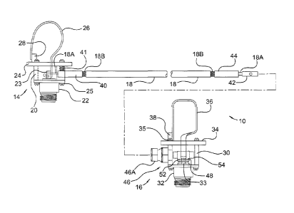
23 [0018] Figure 2 shows a side view of phase cancellation circuit
10, while Figure 3 shows an
24 exploded perspective view of the phase cancellation circuit. The
following description should be
read in view of Figures 2 and 3. Phase cancellation circuit 10 is used in
conjunction with a cavity
26 filter, such as cavity filter 2 shown in Figure 1. Phase cancellation
circuit 10 includes sampler loop
27 assembly 14 and variable signal injection loop assembly 16 connected by
coaxial cable 18. As will
28 be discussed in more detail infra, the length of cabel 18 is equal to a
half-wavelength of a signal at
29 the frequency that isolation of the signal is desired. The loop
assemblies in Figure 2 are shown so
that the inner components of the assemblies are illustrated in dashed or
hidden lines.
7
22292982.2
CA 02643879 2013-08-16
CA 2,643,879
Blakes Ref: 73750/00003
1 [0019] In one embodiment, the cavity filter is cylindrical, such
as cavity filter 2, but it should
2 be understood that the cavity filter could be rectangular or any other
configuration known in the art.
3 Taking cavity filter 2 in Figure 1, for example, phase cancellation
circuit 10 would be installed by
4 replacing loop assemblies 8 with one of each of loop assemblies 14 and
16. Alternatively stated, a
cavity filter according to the current invention would almost exactly resemble
cavity filter 2, with the
6 exception of loop assembles 14 and 16 being installed in apertures 6
instead of loop assemblies 9.
7 Loop assemblies 14 and 16 would be connected via cable 18.
8 [0020] In a preferred embodiment, cable 18 connects variable
signal loop assembly 16 to
9 sampler loop assembly 14. Cable 18 is preferably a 50-ohm coaxial cable,
as is common in RF
communication. In a preferred embodiment the cable is a readily purchasable,
standard cable,
11 made from a silver plated steel center conductor 18A surrounded
respectively by a dielectric layer,
12 double-braided shield layer 18B, and then jacketed in
polytetrafluoroethylene. Cable 18 and its
13 corresponding layers, particularly layers 18A and 18B, are illustrated
in Figures 2 and 3. It should
14 be apparent that other types of cables are known in the art, and this
particular cable merely
represents a preferred choice of cable.
16 [0021] In a preferred embodiment, connector block 20 is a hollow
box. Aperture 21 enables
17 cable 18 to access the interior of the connector block so the cable can
be soldered to loop 26 and
18 bulkhead connector 22. The connector block also has four thru-holes 25'
on both the top and
19 bottom of the block which are correspondingly threaded to receive screws
25.
[0022] Sampler loop assembly 14 includes connector block 20 which is
connected to
21 bulkhead connector 22 and loop ring 24. In a preferred embodiment the
connector block is secured
22 to each of bulkhead connector 22 and loop ring 24 by four screws 25.
However, it should be
23 appreciated that screws are not necessary, and that in an alternate
embodiment, a different securing
24 means known in the art, such as welding or soldering, could be
substituted.
[0023] Loop 26 is shown extending out of hole 27 in loop ring 24 and
affixed to grounding
26 pin 28. In a preferred embodiment, grounding pin 28 is soldered to both
loop ring 24 and loop 26.
27 Loop ring 24 includes four apertures 25" for aligning with apertures 25'
and engaging with screws 25
28 to secure the loop ring to the connector block. Loop ring 24 also
includes hole 43' which is aligned
29 with threaded bore 43 in connector block 20 for set screw 41. In a
preferred embodiment loop ring
24 and grounding pin 28 are silver plated brass.
8
22292982.2
CA 0 2 6 4 3 8 7 9 2013-08-16
CA 2,643,879
Blakes Ref: 73750/00003
1 [0024] In a preferred embodiment, sleeve 40 is soldered to
double braided shield 18B of
2 cable 18 and secured to block 20 by set screw 41. In a preferred
embodiment set screw 41 is a 4-40
3 set screw. It should be appreciated that other varieties of cabling which
do not include a double
4 braided shield layer could be substituted for cable 18, but that a double-
braided cable is preferred.
Furthermore, sleeve 40 could be secured to cable 18 by any other suitable
method know in the art.
6 [0025] The end of loop 26 which extends inside of connector
block 20 is soldered to
7 connector pin 23 of bulkhead connector 22. In a preferred embodiment,
loop 26 is secured by
8 soldering. Also, cable 18 is partially stripped so that a portion of the
center conductor 18A of cable
9 18 protrudes out of sleeve 40 into block connector 20. This portion of
center conductor 18A of cable
18 is illustrated partially hooked around center pin 23. In a preferred
embodiment, the center
11 conductor 18A is soldered to loop 26 and connecting pin 23 of bulkhead
connector 22.
12 [0026] Variable signal injection loop assembly 16 includes
connector block 30 which is
13 connected to bulkhead connector 32 and loop ring 34 by a total of eight
screws 35. As discussed
14 supra with respect to screws 25, an alternate embodiment may include a
different means for
securing the connector block to the loop ring and bulkhead connector. Loop 36
is shown extending
16 out of hole 37 in loop ring 34 connecting to grounding pin 38. In a
preferred embodiment, grounding
17 pin 38 is soldered to loop ring 34 and loop 36. It should be appreciated
that loop ring 34 and
18 grounding pin 38 are substantially identical to loop ring 24 and
grounding pin 28, with the exception
19 of set screw hole 43 located in loop ring 24. Likewise, loop ring 34
includes four apertures 35" for
aligning with apertures 35' and engaging screws 25 to secure the loop ring to
the connector block.
21 [0027] In a preferred embodiment, connector block 30 is a hollow
rectangular box similar to
22 connector block 20. Aperture 31 is included to enable cable 18 and
voltage probe 42 to access the
23 interior of connector block 30 so the voltage probe can rest within
dielectric tube 52 and create a
24 field coupling with coupling tube 48. The connector block also has four
thru-holes 35' on both the
top and bottom of the block which are correspondingly threaded to receive
screws 35.
26 [0028] In a preferred embodiment, loop 36 is a piece of copper
strap which must be bent
27 into the loop shape and twisted 90 degrees so that the loop can be
affixed to coupling tube 48. In a
28 preferred embodiment, loop 36 is soldered to the coupling tube, but it
should be appreciated that
29 other methods known in the art, such as bolting or screwing the loops to
the coupling tube may also
suffice. Coupling tube 48 has aperture 50 to provide access into the coupling
tube from the central
31 pin 33 on bulkhead connector 32. Coupling tube 48 rests on spacer 52.
Spacer 52 is a non-
32 conductive ring that surrounds central pin 33, and in a preferred
embodiment is made of
9
22292982.2
CA 02643879 2013-08-16
CA 2,643,879
Blakes Ref: 73750/00003
1 polytetrafluoroethylene. Dielectric tube 54 is also non-conductive and
fits inside coupling ring 48.
2 Voltage probe 42 is housed within dielectric tube 54 when voltage probe
42 is inserted into variable
3 signal injection loop assembly 16 and held in place by sleeve 44 being
clamped in shaft lock 46.
4 [0029] Voltage probe 42 includes a longitudinal bore which
allows the probe to fit over and
center conductor 18A of cable 18. In a preferred embodiment the voltage probe
is a portion of brass
6 rod with copper and silver plating. In a preferred embodiment, probe
coupling tube 48 is a hollow
7 brass tube. As discussed supra, dielectric tube 54 fits snugly inside
probe coupling tube 48. The
8 dielectric tube aids in the creation of a field coupling between the
voltage probe and the coupling
9 tube when a signal is passed through the filter.
[0030] One end of cable 18 is stripped of the jacketing material and double-
braided shield
11 18B is soldered directly to sleeve 40. In a preferred embodiment sleeve
40 is partially inserted into
12 aperture 21 in the side of block connector 20 and secured inside of
connector block 20 with set
13 screw 41. The opposite end of cable 18 terminates in voltage probe 42.
Voltage probe 42 inserts
14 inside of connector block 30. Similar to sleeve 40, sleeve 44 is
soldered to the double-braided shield
of cable 18. Sleeve 44 in combination with shaft lock 46 enables voltage probe
42 to be variably
16 inserted into connector block 30, so that the voltage probe can create a
field coupling with coupling
17 tube 48 and dielectric tube 54. The sleeves are fabricated from a rigid
material, such as a metal,
18 and are included to enable the cable to be tightly clamped in place by
set screw 41 and shaft lock
19 46.
[0031] Shaft lock 46 is operatively arranged so that it can selectively
secure cable 18, and
21 therefore voltage probe 42, in place. In a preferred embodiment, shaft
lock 46 is operatively
22 arranged to clamp down on sleeve 44 when a threaded hex nut 46A included
on the shaft lock is
23 tightened. The threaded hex nut can also be loosened to release sleeve
44. It should be
24 appreciated that other methods of variably positioning the end of cable
18 connector block 30 could
be used, and shaft lock 46 represents only a preferred means for selectively
securing the voltage
26 probe within block connector 30.
27 [0032] Bulkhead connectors 22 and 32 are bi-directional and can
be used as inputs into the
28 cavity filter, or outputs out of the cavity filter. In a preferred
embodiment, the bulkhead connectors
29 are standard electronic components which are readily purchasable and
known in the art. In a
preferred embodiment, connector 22 receives an input signal to the cavity
filter while connector 32
31 transmits an output signal from the cavity filter. However, it should be
appreciated that there are
22292982.2
.õ
CA 02643879 2013-08-16
CA 2,643,879
Blakes Ref: 73750/00003
1 many styles of receptacles and connectors, and any other input or output
connection means known
2 in the art could be used.
3 [0033] In a preferred embodiment the loops are soldered to their
respective grounding pins.
4 However, it should be appreciated that some embodiments do not include
grounding pins, but
instead the loops are directly bolted or screwed to the loop rings, or use
some other means known in
6 the art to affix the loops to the loop rings for grounding purposes. It
should be appreciated in a
7 preferred embodiment, soldering is the method of affixing all electrical
components in the phase
8 cancellation circuit, but that this only represents a single preferred
method.
9 [0034] As discussed supra, cable 18 is a standard cable known in
the art, and has several
components, including center conductor 18A, a dielectric layer, double braided
shield 18B, and a
11 jacketing. In a preferred embodiment, portions of the cable are stripped
or exposed so the cable can
12 be soldered to different components. For example, as discussed supra,
the double braided shield is
13 soldered to sleeves 40 and 44, and the center conductor is soldered to
pin 23 of bulkhead connector
14 22.
[0035] The purpose of cable 18 is to transfer a sampled portion of the
input signal at a
16 desired isolation frequency to the output of the cavity filter 180
degrees out of phase. By desired
17 isolation frequency we mean the frequency at which a user desires to
position a notch, or achieve
18 isolation. When combined with the input signal, the 180 degree phase
shifted sample signal, or
19 cancellation signal, cancels the input signal at the desired isolation
frequency. Effectively, this
results in a notch at the desired isolation frequency.
21 [0036] In order to achieve the 180 degree phase shift, the
length of cable 18 is determined
22 such that it is equal to a half-wavelength, or a multiple of the half-
wave length of the desired isolation
23 frequency. At low frequencies, the half wavelength is sufficiently long
to enable the cable to connect
24 the variable signal injection and sampler loop assemblies. At higher
frequencies, however, the half-
wave length shortens, and it becomes physically impossible to connect the
sampler loop assembly
26 to the variable signal injection loop assembly with a length of cable
equal to only one half-wave
27 length. Therefore, multiples of the half-wave must be used to provide
the proper length of the cable.
28 [0037] Figures 4A and 4B are front views of variable signal
injection loop assemblies 16
29 which include grounding pins located at two alternate, opposite
locations. Figure 4A shows
grounding pin 28 on the opposite side from where cable 18 is inserted into the
connector block, while
31 Figure 4B shows grounding pin 28 on the same side as the insertion of
cable 18. Varying the
11
22292982.2
CA 02643879 2013-08-16
CA 2,643,879
Blakes Ref: 73750/00003
1 position of the grounding pin will effect the performance of the phase
cancellation circuit, as
2 discussed below.
3 [0038] Figures 5-8 are diagrams of the theoretical performance
of a band pass cavity filter
4 including to phase cancellation circuit 10, illustrating notch 70 at a
frequency above pass band 72.
In the shown example, pass band 72 occurs a range of frequencies surrounding
460MHz. The
6 notch will flip to the opposite side of the pass band for each
incremental half-wavelength that is
7 added to the length of the cable. For example, if the cavity filter is
arranged so that the notch is
8 above the pass band, as shown in Figure 5, increasing the cable by
another half-wavelength will
9 produce a notch below the pass band, such as shown in Figure 6. By below
the pass band we
mean at a lower frequency than the pass band frequency, and similarly, by
above we mean at a
11 higher frequency than the pass band frequency. It should be appreciated
that the diagrams of
12 Figures 5-8 are included for explanation purposes only and should in no
way limit the current
13 invention.
14 [0039] By varying the position of the grounding pin from the
arrangement in Figure 4A to the
arrangement in Figure 4B, notch 70 will alternate between the low and high
sides of the pass band,
16 respectively. It should therefore be appreciated that switching the
position of the grounding pin,
17 such as from the arrangement in Figure 4A to Figure 4B, will change the
position of the notch,
18 without requiring a change in the length of cable 18. That is,
alternating the position of grounding pin
19 28 from the arrangement of Figure 4B to the arrangement of Figure 4A
will produce notches on
opposite sides of the pass band. This behavior is generally depicted by
Figures 5 and 6 which show
21 notch 70 on the high side and low side of pass band 72, respectively.
22 [0040] Figures 6-8 are diagrams showing a theoretical
performance of a bandpass filter
23 including phase cancellation circuit 10, that results from moving the
position of voltage probe 42
24 incrementally out from connector block 30. That is, the relative
position of the voltage probe to the
coupling tube affects the resulting field coupling, which in turn affects the
performance of the phase
26 cancellation circuit. Figure 6 shows the theoretical performance of the
cavity filter with phase
27 cancellation circuit 10 when the voltage probe is deeply inserted into
connector block 30, and
28 therefore the coupling tube. This produces notch 70 close to pass band
72, and the notch is
29 inherently narrow in bandwidth exhibits limited attenuation.
[0041] As the cable and voltage probe are incrementally pulled out of the
connector block,
31 the performance of which is shown progressively in Figures 6-8, it can
be seen that the notch 70
12
22292982.2
CA 0 2 6 4 3 8 7 9 2013-08-16
CA 2,643,879
Blakes Ref: 73750/00003
1 moves away from pass band 72, and the notch becomes wider in bandwidth,
with increasing
2 attenuation.
3 [0042] Therefore, it should be appreciated that by altering the
length of the cable, shifting
4 the grounding pins, and changing the position of the voltage probe with
respect to the coupling tube,
the phase cancellation can be achieved over a broad frequency range, above or
below the cavity
6 filter pass band. Alternatively stated, the notch created by the phase
cancellation circuit is tunable.
7 [0043] Thus, it is seen that the objects of the present
invention are efficiently obtained,
8 although modifications and changes to the invention should be readily
apparent to those having
9 ordinary skill in the art, which modifications are intended to be within
the scope of the invention as
claimed. It also is understood that the foregoing description is illustrative
of the present invention
11 and should not be considered as limiting. Therefore, other embodiments
of the present invention are
12 possible without departing from the scope of the present invention as
outlined in the appended
13 claims.
14
13
22292982.2