Note: Descriptions are shown in the official language in which they were submitted.
CA 02644283 2008-08-29
WO 2007/103274
PCT/US2007/005531
OPTICALLY ADDRESSED SPATIAL LIGHT MODULATOR AND METHOD
TECHNICAL FIELD:
[0001] This
invention relates to optically addressed spatial light modulators
(OASLMs), sometimes termed light valves.
BACKGROUND:
[0002] There
are several distinct technological approaches for generating a
visible light display, particularly large size displays such as those
characterized as large
screen televisions. Liquid
crystal displays generally exhibit high resolution and
advantageous thinness (e.g., about 3 inches). These are typically limited to
sizes of 42"
(diagonal) or less due to cost constraints and the fact that a drive current
cannot be easily
maintained along a very long amorphous silicon row or column drive line,
requiring
significantly complex drive electronics. Liquid crystal displays suffer from
the drawback
that a single pixel can significantly deteriorate resolution over the entire
display; large
sheets of glass have fewer large panels, so the yield loss is highly non-
linear and decreases
with display size.
[0003] Another
technology for large displays is plasma television,
commonly commercially available in the range of 42 to 50 inches. While plasma
offers
good thinness (e.g., 4 inches) and a wide viewing angle, resolution is not as
sharp as other
technologies, the expensive addressing electronics balance bit depth against
resolution
rather than maximizing both, they are generally heavier and suffer from 'burn
in' at the
display screen over time, and they suffer from the same single-pixel shortfall
as liquid
crystal displays. While some research is ongoing into using organic LEDs
(OLEDs) in
large displays, these typically have a lifetime of about 8000 hours or less
for such high-
power applications and are seen as inherently limited.
1
=
CA 02644283 2008-08-29
WO 2007/103274
PCT/US2007/005531
[0004] Front
and rear projection television is becoming more popular as
they overcome some of the above problems with liquid crystal and plasma
technologies.
Projection systems enable screen sizes of 100 inches or greater, and typically
suffer from
resolution and/or brightness (e.g., contending with ambient light for a very
large screen).
Light valves are at the heart of projector systems, mixing shades of different
colored light
(e.g., red, green and blue) to produce a full spectrum of color in the
displayed image.
High temperature polysilicon (HTPS) implementations, such as those marketed by
Seiko,
Epson and Sony, generally use an arc lamp for illumination yet still exhibit
low brightness
at the display due to aperture constraints (ratio of light to area of
reflection) and parasitic
diffraction. Further, resolution in the more commercially popular models is no
better than
that of plasma.
[00051 Liquid
crystal on silicon (LCoS) light valves are used by Sony,
JVC, and a host of other manufacturers, in a relatively small segment of the
large display
market. While these improve brightness and even resolution over HTPS
technology for
little additional cost, they also use an arc lamp for illumination to overcome
light losses
between the arc lamp and the display. It is not unusual for light losses in
LCoS to be 35%
or more, due to aperture, parasitic diffraction, and aluminum reflectivity.
The inventors
see such losses as inherent in the LCoS technology, because much light is lost
between
'tiles' (typically discrete aluminum reflectors) and an even greater amount is
lost by
diffraction from those tile boundaries.
[0006] Digital
light processing (DLP), a technology for which Texas
instruments is well known, also uses an arc lamp and generates mid-range
brightness but
lesser resolution than LCoS. DLP exhibits even higher light losses than LCoS,
due to a
spinning 'color wheel' in addition to micro-reflectors that impose loses
similar to the
LCoS tiles. The color wheel is seen as necessary for DLP in order to operate
with a single
light valve; multiple light valves for different colors are seen to drive
costs high enough
that DLP would not be commercially competitive with other technologies.
[0007] Each of
HTPS, LCoS and DLP dispose the addressing electronics
directly below the modulating surface. This leads to two competing concerns.
First, large
area CMOS dies for the drive electronics are highly expensive; increasing CMOS
chip size
is highly non-linear with cost. Second, optics require that the modulating
surface be large
2
CA 02644283 2008-08-29
WO 2007/103274
PCT/US2007/005531
enough to collect sufficient light to drive a large display with sufficient
resolution and
brightness. The confluence of drive electronics and the modulating plane as
above result
in low yield and high cost for manufacturing HTPS, LCOS and DLP projectors.
What is
needed in the art is a technology that enables large screen displays (e.g.,
greater than about
42 inches) with good resolution and brightness, without the tradeoffs above
between the
size of the CMOS chip and the optical modulating surface that drive up costs
in the current
technology.
SUMMARY: .
[0008] In
accordance with one embodiment of the invention is an optical device
that includes the following layers in the described order. An electrically
insulating first
barrier layer is disposed over a first electrode layer, and a photoconductive
layer is
disposed over the first barrier layer. A carrier confining layer is disposed
over the
photoconducting layer. The carrier confining layer defines a volume throughout
which a
plurality of carrier traps are dispersed. An electrically insulating second
barrier layer is
disposed over the carrier confining layer, and a light blocking layer is
disposed over the
second barrier layer for blocking light of a selected wavelength band. A
reflective layer is
disposed over the light blocking layer for reflecting light within the
selected wavelength
band, a birefringent or dispersive layer is disposed over the reflective
layer, and an
optically transmissive second electrode layer is disposed over the
birefringent or
dispersive layer. The term 'disposed over' does not imply that the layers must
be bonded
to one another directly; intervening layers may be interposed between the
above described
layers as detailed further below.
[0009] In
accordance with another embodiment of the invention is a method for
making a multi-layered optical device. In this method, a first conductive
layer. is provided
and over that first conductive layer is grown a gallium arsenide GaAs layer at
a
temperature less than about 425 degrees C. An electrically insulating layer is
disposed
over the GaAs layer, a photoconducting layer is disposed over the electrically
insulating
layer, and a light blocking layer is disposed over the photoconducting layer.
The light
blocking layer blocks light of a selected wavelength band. A reflective layer
is disposed
over the light blocking layer, and the reflective layer reflects light of the
selected
wavelength band. A birefringent layer or a dispersive layer is disposed over
the reflective
layer, and an optically transmissive second conductive layer is disposed over
the
3 =
=
CA 02644283 2008-08-29
WO 2007/103274
PCT/US2007/005531
birefringent or dispersive layer. As with the optical device above, the
terminology that a
layer is disposed over another layer is not to imply that the disposed layer
necessarily must
be in contact with the layer over which it is disposed; intervening layers are
possible
without departing from these teachings, and several such intervening layers in
addition to
those detailed above are particularly described below.
BRIEF DESCRIPTION OF THE DRAWINGS:
[0010] The
foregoing and other aspects of these teachings are made more
evident in the following Detailed Description, when read in conjunction with
the attached
drawing figures.
[0011] Figure
IA is a schematic cutaway view showing some of the
distinct layers of an Optically Addressed Spatial Light Modulator (OASLM)
according to
an embodiment of the invention.
[0012] Figure
1B is a schematic diagram similar to Figure IA, but showing
a different embodiment.
[0013] Figure
IC is a schematic diagram similar to Figure IA, but showing
yet another embodiment.
[0014] Figures
2A-C are schematic diagrams illustrating movement and
trapping of electrons and holes within the layered light valve of Figure 1A.
[0015]
Figures 2D-2E are schematic diagrams similar to Figure 2C but
showing electrons and holes pairing in the respective second and first carrier
confining
layer.
[0016] Figure
2F is an equivalent circuit representing certain layers in the
light valve of Figure IA.
[0017] Figures
3A-3C are similar to Figures 2B-2C and 2E respectively,
but for the embodiment of Figure 1B.
=
4
CA 02644283 2008-08-29
WO 2007/103274
PCT/US2007/005531
[0018] Figure
4 is a time-versus temperature growth profile for several of
the lower layers of the embodiment of Figure IA.
[0019] Figure
5 is a schematic diagram of a single spatial light modulating
valve in conjunction with an optical engine for together forming a projected
image.
[0020] Figure
6 is a schematic diagram of three spatial light modulating
valves in conjunction with one type of optical engine for together forming a
projected
image.
[0021] Figure
7 is a schematic diagram of three spatial light modulating
valves in conjunction with another type of optical engine for together forming
a projected
image, and also showing a prior art arc-lamp source overlain for comparison
purposes.
[0022] Figure
8 is another embodiment of an optical engine configured to employ
an OASLM according to these teachings.
=
DETAILED DESCRIPTION:
[0023]
Optically addressed light valves offer several advantages over other
large-screen commercial imaging technologies such as MEMS, liquid crystal on
silicon, or
High Temperature Polysilicon. For example, certain embodiments of this
invention offer
significant cost advantages over these technologies. Light valve embodiments
described
herein are able to preserve etendue to a much more significant level than
projection
technologies using color sequential modulation or multiple light valve systems
with
limited surface area such as is the case with liquid crystal on silicon
displays. Etendue
may be conceptualized as optical throughput efficiency through disparate
optical devices.
When a light source is coupled to an optical engine, &endue is a measure of
the optical
efficiency of that coupling. If the source is a laser, etendue may generally
be readily
preserved. Where the source is non-point as are commonly used in large-screen
imaging
arts, etendue becomes a significant factor because optical coupling from a non-
point light
source to a modulator is typically very poor largely because the modulator is
generally
small (e.g., a chip measuring less than 0.9 inches in diagonal), so light not
directly
impinging upon the modulator is lost if not effectively managed for etendue.
Merely
CA 02644283 2008-08-29
WO 2007/103274
PCT/US2007/005531
enlarging the silicon-based chip size is not cost effective because to do so
would reduce
the number of chips made from a single wafer, effectively reversing some of
the
efficiencies that drive Moore's law of continually decreasing cost per chip.
The relation
between chip size and cost is not a linear one; doubling chip size more than
doubles the
cost of that larger chip, typically much more than double. Generally, the
prior art uses a
high power white light source such as an arc lamp, whose light is then
modulated and
pixilated, to overcome poor &endue by its sheer optical output power. But an
arc lamp
runs very hot and requires routine bulb replacement. Embodiments of this
invention
provide a more elegant solution than merely increasing wattage at the light
source.
Further, optically addressed light valves avoid the constraint of other
technologies that the
addressing electronics lie directly below the modulating optical plane. This
is detailed in
the Background section, and leads to higher cost and lesser performance due to
the
tradeoff between sizes of the CMOS electronics chip and the optical modulating
plane.
[0024] Figure
IA illustrates in sectional view an OASLM 20 optical device
according to an embodiment of the invention. Relative layer thicknesses of
Figures IA or
1B are not to scale nor are they proportional relative to one another; Figures
1A-1C are for
illustration of the various layers as distinct entities. As the embodiments of
Figures 1A-1C
are forward addressed (from the top), the various layers are detailed below in
the order of
top to bottom. Figure IA is described with specificity, Figure 113 is
described with respect
to its differences over Figure 1A, and Figure IC is described with respect to
its differences
over Figure 1B.
[0025] In
Figure 1A, a protective overlayer 22 forms a front surface 22a of
the OASLM 20 to protect the underlying layers, and is substantially
transmissive to light
in both the visible and infrared (112) bands. Glass, sapphire, quartz, SiC,
ZnO, and GaP are
exemplary but not exclusive materials from which the protective overlayer 22
may be
formed. Beneath the protective layer 22 is a transmissive conductor 24 that is
electrically
.conductive and transmissive to light in the visible and IR bands.
Transmissive conductive
layers are known in the art (See for example, US Pat. 5,084,777; "PROGRESS IN
LIQUID
CRYSTAL LIGHT VALVES" by W. P. Bleha in Laser Focus/Electro-Optics, October
1983;
and "DEVELOPMENT OF GALLIUM ARSENIDE-BASED SPATIAL LIGHT MODULATORS" by
Michael C. Hebbron and Surinder S. Makh in PSIE vol. 825 Spatial Light
Modulators and
Applications II, 1987). An exemplary material for the conductive layer is
indium tin oxide
6
CA 02644283 2012-05-02
(commonly ITO), which is essentially transparent to visible light and
attenuates IR light
only slightly. The conductive layer 24 substantially spans a cross section of
the OASLM
20 in order to provide a relatively uniform charge across the entire cross
section.
[0026] Below the transparent conductive layer 24 is a birefringent or
dispersive layer 26, such as liquid crystals, bismuth oxide, or other
materials whether
crystalline in structure or not that can modulate light. The distance between
layers 24 and
26 is called the cell gap wherein layer 26 is substantially uniform and
important as this
layer defines the modulation of the light when the OASLM 20 is in operation.
Flanking
each major surface of the birefringent/dispersive layer 26 (i.e., both above
and below the
birefringent/dispersive layer 26 as illustrated in Figure 1A) is an alignment
layer 27a, 27b,
for anchoring layer 26. An exemplary material for the alignment layers is
silicon oxide
SiOx. As will be shown, since the light to be modulated passes twice through
the
birefringent/dispersive layer 26, this layer need only modulate the read light
half as much as
for a single pass device and as such can be thinner increasing switching speed
and
resolution.
(0027] Below the birefringent/dispersive layer 26 is a distributed
Bragg
reflector DBR 28 or cold mirror layer, more generally a reflective layer
comprised of
dielectric materials that is reflective within a selected wavelength band. In
one
embodiment, addressing light is infrared and the modulated read light is
visible, so the
013R layer 28 reflects or block light in the visible band yet allows selected
spectral
wavelengths of IR light to pass relatively unobstructed. The DBR layer 28 may
be readily
tuned to pass only a particular TR band of interest, so that of all light
entering the OASLM
20 from the front surface 22a (e.g., the modulated read light and addressing
light), only the
IR. light within the bands of interest is allowed to transmit through the DBR
layer 28. The
DBR layer 28 can be adjusted by design of the DBR layer 28 itself to form a
notch or band
pass filter for specific IR wavelengths or in combination with the light
blocking layer
(LBL). As an alternative, the embodiment of Figure 1B shows a first DBR layer
28a
similar to the DBR layer 28 described above with reference to Figure IA,
deposited over
an LBL 30 of potentially lesser thickness than would typically be used with
the
embodiment of Figure IA, which in turn is deposited over a second DBR layer
28b. as
compared to Figure 1A, this embodiment adds a second DBR layer 28b between the
LBL
30 and the first barrier layer 36a.
7
CA 02644283 2008-08-29
WO 2007/103274
PCT/US2007/005531
[0028) As will
be detailed below, each IR band of interest for addressing
light can be considered to address a specific spectral width of light in the
output image,
called the read light, for which that particular IR band addresses. In an
exemplary
embodiment, the DBR 28 (or DBRs 28a, 28b) is (are) made from alternating
layers of
materials having a different refractive index for given wavelengths of
interest, such as
titanium dioxide TiO2 and silicon dioxide Si02, or aluminum arsenide AIAs and
gallium
arsenide GaAs. In either implementation the DBR can be made of a variety of
materials
including but not limited to Nb05, Si02, Ti02, Ta205, ZnSe, AlAs, GaAs, etc.
While these
descriptions are in the context of IR addressing light and visible read light,
these
wavelength bands are exemplary; read light may be for example UV or IR,
leading to
different materials used to form various layers in the light valve in order to
block/reflect
the wavelength bands for the non-visible read light.
[0029)
Returning to Figure 1A, a light blocking layer 30, separate and
distinct from the DBR layer 28, lies below the DBR layer 28 to further block
any visible
light, that may pass, since the DBR layer 28 may be less than 100% efficient
in reflecting
visible light (or other light outside the intended pass band). The light
blocking layer 30
also may be tuned to transmit or partially absorb selected IR bands of
interest by selecting
a material with an appropriate indirect or direct bandgap. The light blocking
layer 30 is
generally about 1 micron thick and acts as an optically invariant electrical
component.
That is, depending on the kind of electric field applied across the device the
capacitance,
resistance and or impedance of the light blocking layer 30 does not vary with
the intensity
of light incident upon it. Were it to be otherwise, the light blocking layer
30 would have
varying electrical properties that would induce unintended light modulation at
layer 26 in
the embodiments of Figures 1A-1B, making the overall performance of the device
ineffectual. A favorable characteristic of the light blocking layer 30 is that
any charge
carriers generated therein are short lived. The material of the light blocking
layer 30 is
selected to be highly absorbing for spectra with an energy greater than the
bandgap of that
material (if the material has a bandgap). The light blocking layer 30 may be
made from a
low temperature material (see the description below for the carrier confining
layers 34a,
34b) or even low quality AlGaAs, InGaAs, GaAs, a-SiGe:H, CdTe, or for example
fine
grained polycrystalline or deposited GaAs, such that any charge carriers
(e.g., holes or
electrons) generated by the absorption of spectra within the energy range
above the
=
8
CA 02644283 2012-05-02
bandgap are short lived (e.g., they do not separate under the applied electric
field across
the electrodes 24, 38), and therefore do not significantly modulate the
capacitance,
resistance or impedance of the light blocking layer 30.
[0030] A photoconducting layer 32, shown in Figure IA as having a
first
carrier confining layer 34a and an optional second carrier confining layer 34b
adjacent to
its respective opposed major surfaces, is located below the light blocking
layer 30 and is
where the addressing IR light is converted to electrical charge carriers
(holes and
electrons). Due to the reflection of visible light at the DBR layer 28, and
absorption or
reflection at the light blocking layer 30 of light outside the pass band that
passes the DBR
layer 28, IR light within the selected band of interest passes to excite the
photoconductor
portion 32 of the photoconductor layer. Any read light that does reach
photoconducting
layer 32 will likely generate carriers and as such the change in capacitance,
resistance and
or impedance of this layer as affected by the residual read light reaching it
must generate a
voltage across the birefringent layer 26 below its threshold voltage so as to
not cause
modulation of the read light at that layer.
[0031] An exemplary material for the photoconducting layer 32 is
high
quality gallium arsenide GaAs, possibly ranging in In and Al mole fractions
from InGaAs
to AlGaAs. This layer 32 can range in thickness up to tens of microns, and
some
exemplary embodiments define a much lesser thickness on the order of hundreds
of
nanometers to microns (e.g., 100 or 200 nms to 2 or 5 microns) which increases
resolution
as compared to thicker hydrogenated amorphous silicon photoconductive layers.
These
lesser thicknesses are thinner than prior art photoconductor layers that use a
rear-
= addressing regimen. Note however that it is possible to address the
devices of the type
described herein from the rear as well by using appropriately Selected
addressing spectral
wavelengths and or by removing the bottom wafer and bonding the remainder of
the
structure to a material that is essentially transparent to the selected
addressing spectra.
Most of the photoexcitation occurs in the first two microns of the
In/GaAsiGaAs/AlGaAs
photoconductor material with its high absorption properties upon which the
incident light
impinges. AlGaAs and GaAs are preferred for the photoconducting layer 32 for
manufacturing efficiency, as will be detailed below in conjunction with the
first carrier
confinement layer 34a (and second carrier confinement layer 34b) and the
substrate 40.
9
CA 02644283 2008-08-29
WO 2007/103274
PCT/US2007/005531
[0032] The
first carrier confining layer 34a lies nearer the visible light
blocking layer 30 (as compared to the second carrier confining layer 34b), and
is
impregnated with arsenic precipitates (or a distribution of some other energy
barrier
nodes) that substantially impede movement of the charge carriers near the
junction
between the carrier confining layer and the insulating layer 36a. The second
carrier
confining layer 34b lies nearer the substrate 40, and is also impregnated with
arsenic
precipitates or a plurality of some other energy barrier nodes that
substantially impede
movement of the charge carriers near the junction between the carrier
confining layer and
the insulating layer 36b. The total thickness of each carrier confining layer
34a, 34b is
preferably between about five and twenty nanometers in one embodiment. High
thickness
for the carrier confining layers 34a, 34b would render the confining layers to
absorb
significant energy destined for the photoconductor which is undesirable.
Thinner
dimensions for the carrier confining layers 34a, 34b ensure that it is not
optically active
and that the charge carriers are well trapped by the As precipitates.
[0033] An
exemplary material for the carrier confining layers is commonly
termed low temperature grown gallium arsenide denoted as LTG-GaAs, low
temperature
grown indium gallium arsenide denoted as LTG-InGaAs and/or low temperature
grown
aluminum gallium arsenide denoted as LTG-AlGaAs. LTG-GaAs, as well as the
other
LTG materials, is grown at a lower temperature than 'normal' GaAs (or other
materials),
typically within the range of about 200-300 degrees C, whereas 'normal' GaAs
is typically
grown at a temperature in the range of about 500-600 degrees C. In some
contexts,
intermediate grown temperature GaAs, referred to as ITG-GaAs, is grown in the
temperature range of about 375-425 degrees C. Note that the above are inexact
ranges; the
terms LTG-GaAs and ITG-GaAs are known in the art but not precisely defined by
temperature. The
second carrier confining layer 34b is optional, and either or both
carrier confining layers 34a, 34b may range in thickness from about five to
twenty
nanometers in exemplary embodiments to assure that the carrier confining layer
is not
optically active. Figure 1B illustrates an embodiment absent the lower or
second carrier
confining layer 34b, and its operation is further detailed with respect to
Figures 3A-3B
below.
[00341 A
separate interface between the carrier confining layers 34a, 34b
and the photoconductive layer 32 may grade the transition. For example, layers
of indium
CA 02644283 2012-05-02
gallium arsenide InGaAs and/or AlGaAs may be disposed between the GaAs
photoconductive layer 32 and either or both of the carrier confining layers
34a, 34b,
compositionally graded from pure GaAs at the photoconductive layer 32 to a
mole fraction
of AlGaAs or InGaAs along the transition (distinct transition layers not
shown) and
turning into LTG-GaAs, LTG-InGaAs and/or LTG-AlGaAs at the carrier confining
layers
34a, 34b. In one embodiment it may be preferable to have the carrier confining
layer made
of LTG-AlGaAs with compositional grading to a tuned photoconductive layer 32
which
may be made of AlGaAs, GaAs or InGaAs, as the As precipitates in LTG-AlGaAs
are
deeper level and as such form even greater traps of carriers. Another
embodiment may
have compositionally graded series of layers of AlGaAs, GaAs and/or InGaAs and
their
LTG counterparts to tune the resistance and/or capacitance of the
photoconductive layer.
[00351 An optional first barrier layer 36a lies between the first
carrier
confining layer 34a and the light blocking layer 30. This prevents charge
carriers, trapped
within the first carrier confining layer 34a from migrating toward the light
blocking layer
30 and the birefringent layer 26. A second optional barrier layer 36b lies
between the
second carrier confining layer 34b and a lower electrode layer 38. The second
barrier
layer 36b prevents charge carriers from migrating between the lower electrode
38 and the
photoconducting layer 32 or second carrier confining layer 34b depending on
whether the
optional carrier confining layer 34b is present. The barrier layers 36a, 36b
may or may not
be made from the same material as one another, An exemplary material for the
barrier
layers 36a, 36b is any insulating material compatible with adjacent layers,
such as
aluminum gallium arsenide AlGaAs, aluminum arsenide AIAs, or any dielectric
material.
[00361 The lower electrode layer 38 may be any conductor, and for a
forward addressed embodiment as shown in Figure IA the lower conductor 38 need
not be
optically transmissive. Exemplary materials for the lower conductor layer 38
include
doped GaAs, doped AlGaAs (of any of various mole fractions of Al), doped
InGaAs (of
any of various mole fractions of In), doped Galra) lattice matched to GaAs, or
a
conductive oxide such as indium tin oxide (commonly ITO) deposited after
removal of the
GaAs substrate used for the epitaxy of the device, or in fact it may be the
substrate itself
which can be conductive in which case 38 and 40 are one and the same.
ii
CA 02644283 2012-05-02
[0037] The substrate
layer 40 is preferably a wafer made of GaAs, and may
serve three functions. First, it is a mechanical substrate to support the
overall OASLM 20.
Second, it may act as the lower electrode 38 in opposition to the transmissive
conductor
24. As illustrated in Figure IA, an electric field (preferably AC) is applied
across the
lower electrode 38 and the transmissive layer 24, as will be detailed below.
If a separate
lower electrode layer 38 is disposed as shown in Figure 1A, then any
electrically
conductive properties of the substrate 40 further distribute charge across the
entire cross
section of the OASLM 20. Alternatively, the substrate 40 may act as the sole
lower
conductor and the separate lower conductor and layer 38 is not necessary.
Alternatively
the substrate 40 may be semi-insulating with an electrode corriprised of doped
InGaAs,
GaAs, AlGaAs, InAs, ITO, Au/Ti or other common electrode material deposited
beneath
the substrate with or without an optional insulating layer separating these
comprised of
AlAs, AlGaAs, Si02 or other suitable material. Third, the substrate 40 acts as
a seed layer
from which the GaAs epitaxy is grown (in certain embodiments). In some
embodiments
the GaAs wafer may be removed and the layers grown by epitaxy bonded to a
different
substrate of not. There are several techniques to accomplish this including
but not limited
to polishing, lift off, and chemical separation using a sacrificial layer to
allow for this, to
name a few. The GaAs epitaxy may be used in some embodiments to form the
second
barrier layer 36b AlGaAs), the
second carrier confining layer 34b (e.g., LT-GaAs),
the photoconducting layer 32 (e.g., GaAs), the first carrier confining layer
34a and the first
barrier layer 36a, and even the light blocking layer 30. Of course, other
embodiments may
divide at least the mechanical substrate and lower electrode functions into
distinct layers
and/or use different materials for some layers noted immediately above,
perhaps losing
some efficiencies in manufacturing that arise from growing these various
layers in a single
varying process from the GaAs wafer 40. Other exemplary materials for the
substrate 40
include germanium wafers, silicon germanium on silicon wafers, ZnSe wafers and
InGaP
to name but a few.
[0038] A GaAs wafer
is preferred as the substrate 40 for several reasons.
While silicon is vastly more common, GaAs wafers rank second in commercial
wafer
production volume, so they are readily available. For example, GaAs chips are
currently
used in cell phones (HBTs and pHEMTs) DVD and CD players, and for red LEDs.
From
a commercial perspective, the finished cost per size for GaAs used in. an
OASLM is not
nearly as non-linear as cost per size for silicon chips that incorporate
transistors (such as
12
CA 02644283 2008-08-29
WO 2007/103274
PCT/US2007/005531
for LCoS or DLP technologies). While cost scaling is not quite linear with
surface area,
the cost per chip size relation for an OASLM made of GaAs is quite inexpensive
relative
to similarly sized devices using CMOS such as LCoS and MEMS devices where the
relation is highly non-linear. Increasing chip size is a simple way to
increase &endue in an
overall optical system, and the above cost considerations make a larger GaAs
chip much
more commercially viable than a Si chip (with CMOS electronics) of the
comparably
increased size. From a technical perspective, a molecular beam epitaxy MBE or
metal-
organic chemical vapor deposition MOCVD layer can be readily grown on a
monolithic
GaAs wafer. Current technology does not enable the LTG-GaAs or other LTG-type
layers
with precipitates, as noted herein, to be grown using a MOCVD process, but
rather is
= grown by MBE though there have been reports that this is possible. All
the other epitaxial
layers can be grown by MBE or MOCVD processes. Prior commercialization of GaAs
epitaxy has advanced the art to the point where lattice-matched GaAs epitaxy
can be
grown with good yield, reasonable cost, and high uniformity. Prior art
optically addressed
digital light valves, such as those originally pioneered many years ago by
Hughes
Electronics and Greyhawk Systems , were generally based on amorphous silicon,
using
a sputtering process to deposit hydrogenated amorphous silicon a-Si:H on
Indium Tin
Oxide on glass. Because the layers were thick, and the coefficients of thermal
expansion
of the substrates and electrodes that they were deposited on were different,
cracks often
developed after deposition during cooling.
[0039]
Figure 1C illustrates in schematic form yet another embodiment of the
OASLM 20, with only differences as compared to Figure 1B described in detail
here.
Note that in Figure IC, the lower electrode 38 is disposed below the substrate
40, on the
opposite side as compared to the upper electrode/transmissive conductive layer
24.
Dielectric stack layers 39a, 39b lie on either side of the lower electrode 38,
and a third
barrier/insulating layer 36c is disposed between the lower electrode 38 and
the substrate
40. Like Figure 1A, Figure IC includes only a single DBR layer 28, directly
above the
light blocking layer 30. Also like Figure 1A, Figure IC includes a second
carrier
confining layer 34b disposed on the opposite side of the photoconducting layer
32 as
compared to the first carrier confining layer 34a, whereas Figure 113 includes
only a single
carrier confining layer. In Figure IC, the dielectric stack layers 39a, 39b
are optional, as
are any or even all of the three barrier/insulating layers 36a, 36b, 36c. Both
the second
and third barrier layers 36b, 36c are optional because in some embodiments the
substrate
13
CA 02644283 2008-08-29
WO 2007/103274
PCT/US2007/005531
40 itself may electrically isolate the lower conductor 38 from the second
carrier confining
layer 34b and photoconducting layer 32. As is evident from Figures 1A-1C,
these
different embodiments may be combined to yield different specific layer
structures
according to these teachings without departing from the scope of this
invention; the
various functions and interrelationships of layers are detailed herein to
enable such other
combinations. ,
[0040]
Characteristics of the carrier confining layers 34a, 34b are now
described in detail. After being grown, the carrier confining layers 34a, 34b
are annealed
at a temperature elevated over the temperature at which those layers were
grown. For
example, for LTG-GaAs grown at about 200-300 degrees C, anneal temperature
might be
within the range of about 500-600 degrees C. For LTG-AlGaAs also grown at 200-
300
degrees C the anneal temperature might be within the range of about 600-700
degrees C,
and the anneal may continue for at least about twenty minutes or more. Longer
anneal
periods typically do not adversely affect the desired properties of the
carrier confining
layers 34a, 34b. During the anneal, the arsenic that precipitated out of the
stressed GaAs
lattice during the low-temperature growth phase becomes nearly uniformly
distributed
throughout the volume of the carrier confining layers 34a, 34b, and forms
distinct, nearly
sphere-like nodes. These arsenic precipitates or carrier trapping nodes act as
the metal
component of Schottky barriers in those layers 34a, 34b of the completed OASLM
20,
exhibiting an energy level below that of the electrons and holes in layer 32
preventing
them from migrating, at least for some non-negligible period of time,
laterally or in the
direction of the front surface 22a or substrate 40. A non-negligible period of
time is
considered in the context of the overall OASLM 20. In accordance with
standards
currently controlling in the U.K. and U.S., a video frame must be refreshed
about every
1/24111, 1/50th or 1/60th a second respectively. Embodiments of the invention
refresh the
video frame at double that rate, so a non-negligible constraint on charge
carrier movement
for those 120 Hz embodiments holds the charge carriers in place for at least
I/48th to
1/120111 of a second. Other embodiments with different refresh rates may
operate with a
different cycle rate and therefore define a non-negligible period of time
differently. In
general, the carrier confining layers 34a, 34b, are designed to retain or trap
charge carriers
of one type (holes or electrons depending on the direction of the applied
electric field) for
at least the period of time defined by the cycling frequency of the applied
electric field
across the electrodes 24, 38. Because charge carrier migration is properly
modeled as a -
14
CA 02644283 2008-08-29
WO 2007/103274
PCT/US2007/005531
distribution, the carrier confining layers may be considered to trap a
substantial majority
(e.g., greater than about 85%, preferably greater than about 95%) of charge
carriers of one
type (holes or electrons depending on the direction of the applied electric
field) for that
time period.
=
[0041]
Operation of the OASLM 20 is now described. Preferably, a
polarizing input filter 42 is imposed between the OASLM 20 and an IR
addressing source
44 (addressing light) if using a birefringent modulating layer 26, of which
Figure IA
shows the source 44 as three distinct IR sources one each destined to address
an OASLM
. tuned to modulate either red, green or blue visible light (IRR, IRE, and IRB
respectively).
One addressing source 44 may be used as will be described below with reference
to Figure
5, though any number of addressing sources and/or light valves may be used in
various
embodiments, not necessarily limited to the one or three addressing sources
detailed
herein. For example, more than three color sources and light valves may be
used for
greater precision and efficiency over color control in the projected image.
Such variations
follow readily from the examples shown herein. The input polarizing filter 42
is
preferably reflective and not made in one piece with the OASLM 20.
[0042] The
addressing IR light from the source 44 (which may or may not
be polarized) passes through the glass overlayer 22 and the transmissive
conductor 24
substantially unattenuated. Light outside the selected IR band(s) may be
present, due to
reflection of the visible light that is output from the OASLM 20, from the
source 44 itself,
or from any other source emitter, so design of the OASLM 20 does not presume
only IR
light in the selected bands enters the front surface 22a. The addressing IR
light is passed
through the liquid crystal layer 26. Since the visible light to be modulated
passes through
layer 26 twice, once along the input pathway and once along the output pathway
as will be
described, the thickness of layer 26 may be less than for transmissive light
valves,
preferably by half. The applied electric field across the transmissive
conductor 24 and the
lower electrode 38 (or substrate/wafer 40 as lower electrode or electrode
beneath
substrate/wafer 40) in conjunction with the imposition of the input IR
addressing light that
strikes the photoconducting layer 32 modulates on layer 26. The IR addressing
light can
impose, for example, a pulse width modulation by providing a constant-
amplitude, time-
modulated burst of energy (induced by photons in this instance), determined by
the
interaction or the various layers in the OASLM and the applied electric field.
As tested,
CA 02644283 2008-08-29
WO 2007/103274
PCT/US2007/005531
the inventors were able to achieve 2.1 million squares in the birefringent
layer 26, yielding
2.1 million pixels in the output image. The resolution can be lower by
definition and in
fact substantially higher. The IR addressing light can also be comprised of a
sequence of
light pulses and/or an amplitude and/or time modulated sequence or single
pulse of
energy.
[00431 The IR
addressing light passes from layer 26 through the DBR layer
28 and the light blocking layer 30, which strip nearly all visible light and
in fact most light
from outside the band(s) of interest to which those layers 28, 30 are tuned
from passing
below the light blocking layer 30. The IR addressing light then passes through
the first
barrier layer 36a, the first carrier confining layer 34a and then the
photoconducting layer
32. Because of the thickness of the carrier confining layers 34a, 34b, (e.g.,
preferably
about 5 to 20 nm), they are not optically active or optically responsive.
While optical
responsivity is generally a function of wavelength, for all practical purposes
it is
understood that LTG-GaAs is not optically responsive until its layer thickness
is above
about 100 nm for wavelengths in the visible or IR regions which are above the
bandgap
energy. LTG-GaAs in layer thicknesses less than .about 100 nm cause that layer
to be
optically non-responsive, and no charge carriers are generated from the
addressing light
within that thin layer of LTG-GaAs. In short, the. carrier confining layers
34a, 34b on the
thickness orders described herein are not photoconductive. It is
noted that the
photoconducting layer 32 is not considered to be carrier-trapping; electrons
and holes
migrate freely within that photoconducting layer 32. In terms of the charge
carriers for
certain embodiments then, they are generated only within the photoconducting
layer 32;
they are trapped only in the carrier confining layers 34a, 34b; and upon
reversal of the
applied electric field, the holes drift one direction and the electrons drift
the other direction
and so only one type of carrier ends up in each carrier confining layer. Upon
reversal of
the applied electric field one or both types of carriers are freed to then
recombine with the
opposite carrier that was trapped.
[0044]
Spatially localized electrons and holes within the photoconducting
layer 32, excited by the addressing IR light, are then drifted in opposite
directions of the
photoconducting layer 32 by an applied electric field; electrons toward the
second carrier
confining layer 34b whose flow is opposite to the direction of the applied
electric field and
holes toward thc first carrier confining layer 34a in the direction of the
electric field, or
16
CA 02644283 2008-08-29
WO 2007/103274
PCT/US2007/005531
vice versa depending on the applied electric field direction. This is shown
schematicalfy
for one electrical model interpretation in Figures 2A-2C as a hybrid
schematic/electrical
diagram.
[0045] Figure
2A shows the relevant layers as being static, with no free
charge carriers. The photoconducting layer 32 is made of a high quality
undoped GaAs,
InGaAs and/or AlGaAs materials, which is flanked by the first 34a and second
34b carrier
confining layers. Addressing light, shown in Figure 2A as IR photons hv, enter
the
illustrated layers from the left so as to strike the first carrier confining
layer 34a prior to
the others illustrated in Figure 2A. In Figure 2B, the addressing IR photons
hv impinge
the photoconducting layer 32, freeing charge carriers electrons e" and holes
a+ within that
layer 32. As shown in Figure 2B, the applied electric field causes the holes
(=I+ to move
toward the first carrier confining layer 34a, and the arsenic precipitates
within that layer
34a impede movement of the holes o+ from passing through that layer 34a or
from
migrating laterally within it by trapping them in the carrier confining layer.
Similarly and
simultaneously, the same applied electric field causes the electrons e" to
move toward the
second carrier confining layer 34b, and the arsenic precipitates within that
layer 34b trap
those electrons, impeding movement of the electrons e- beyond that layer 34b
or laterally
across it, so that the opposed electrons e- and holes o+ are trapped at
opposite ends of the
photoconducting layer 32. At Figure 2C, the applied electric field is reversed
(or
otherwise relaxed or modulated), causing the electrons e- and holes o+ from
the opposed
carrier confining layers 34a, 34b to recombine within the photoconducting
layer 32,
clearing the OASLM 20 for the next image frame. Figure 2D shows the electrons
and
holes pairing in the second carrier confining layer 34b, and Figure 2E shows
the electrons
and holes paired in the first carrier confining layer 34a, such as where the
applied electric
field is relaxed rather than reversed. As above, in one embodiment the applied
electric
field is reversed at least as often as a frame refresh rate stipulated in a
video transmission
standard, which in the U.S. is 60 Hz (although other applications may require
faster or
slower frame rates), and the carrier confining layers 34a. 34b are designed to
trap a
substantial distribution of electrons or holes for at least the time period
defined by the
refresh rate (the rate at which the applied electric field is reversed and the
frame image is
refreshed). In an exemplary embodiment, the OASLM 20 reverses applied electric
field at
17
CA 02644283 2008-08-29
WO 2007/103274
PCT/US2007/005531
120 Hz. Other exemplary frequencies include 24 Hz, 50 Hz, 60 Hz, 72 Hz, 120
Hz, and
greater.
[0046] The
carrier confining layers 34a, 34b having arsenic precipitates
acting as Schottky barriers are capable of retaining the electrons e" and
holes o+ in place
for about 50 milliseconds at room temperature, whereas a refresh rate of 60 Hz
requires
only about 16.67 milliseconds. Doubling the refresh rate clearly does not
exceed the
electrical capabilities of the carrier confining layers 34a, 34b. These times
are different
depending on the LTG material selected such as AlGaAs, GaAs and InGaAs.
[0047] These
localized charges from the electrons e" and holes o+ produce a
localized electric field within certain layers of the OASLM 20. These fields
interact with
the externally applied electric field and modulate the localized electric
field nearest layer
26 which is terminated by the transmissive conductor 24 above layer 26 which
in turn
translates an image of the charge packets in the first carrier confining layer
34a to the light
to be modulated.
[00481 One
simplified electrical circuit is shown in Figure 2F (others exist
partially depending on the frequency of the externally applied electric
field), wherein the
photoconducting layer 32 and the birefringent layer 26 are shown as capacitors
in series
between the lower electrode 38 (or substrate 40 as lower electrode) and the
transmissive
conductor 24 as top electrode. Note that each layer of the light valve
illustrated in Figure
lA contributes some capacitance; only those layers relevant to the below
explanation are
represented in Figure 2F. The thickness of the various layers, and their
dielectric
constants, determine that layer's capacitance. As shown in Figure 2F, in this
example
where we assume a 10 V applied electric field, the birefringent layer 26
(nearer the top
electrode 24 of Figures 1A-1B) exhibits a potential drop of about 2 volts
(although this can
be different), whereas the photoconducting layer 32 (nearer the bottom
electrode 38 of
Figures 1A-1B) exhibits a potential drop of about 8 volts (although this can
be different).
As the local impedance, capacitance or localized electrical fields within the
photoconducting layer 32 change the voltage drops from 8 volts to 6 volts, the
excess
voltage goes to layer 26, raising its potential from 2 volts to 4 volts. This
stimulates layer
26 to modulate (assuming the threshold voltage for this layer is between 2 and
4 volts) the
18
CA 02644283 2012-05-02
read light that passed/reflects through it. The above voltage figures are for
illustration; the
light valve may operate in voltage ranges far removed from those noted above.
[00491 Returning to Figure IA, read light 48 (which may or may not
originate from the same source 44 as the IR addressing light) in the visible
range is
directed toward the front surface 22a, and passes into the OASLM 20 into layer
26, which
by Figure 2E now carries the image from the addressing light and
photoconducting layer
32. The read light 48 is prevented from reaching lower layers by the DBR layer
28 and
the light blocking layer 30. The read light 48 may pass through a polarizing
output filter
46 prior to striking the front surface 22a. The read light 48 is modulated at
layer 28,
reflects from the DBR layer 30, is modulated again at the birefringent layer
26 and passes
out again through the front surface 22a (and possibly the polarizing output
filter 46) for
projection as visible (or other wavelength band) light. Transmissive versions
of this
structure are also possible.
[0050] Figures 3A-3C mirror Figures 28-2C and 2E respectively, but
for
the embodiment of Figure lB that lacks the second carrier confining layer 34b
of Figure
IA. With an applied electric field, Figure 3A shows holes drifted toward the
first carrier
confining layer 34a (that nearest the first barrier layer 36a and the light
blocking layer 30)
as with Figure 2B, but the electrons are drifted toward the second barrier
layer 36b. These
electrons generally remain in the photoconductive layer 32 but accumulate
nearer the
major surface of that layer 32 furthest from the first carrier confining layer
34a, and
nearest to the second barrier layer 36b, due to the applied electric field.
Upon reversal,
relaxation, or other modulation of the applied electric field, Figure 3B
illustrates the holes
drifted back into the photoconductive layer 32, and the electrons drifted
either strongly
toward the first carrier confining layer 34a (in the case of reversal of the
applied electric
field) or merely drifted to a more equal distribution throughout the
photoconductive layer
32 (in the case of relaxing the applied electric field). Figure 3C illustrates
that the
electrons that accumulated near the second barrier layer 36b combine within
the first
carrier confining layer 34a with holes that were previously trapped in that
first carrier
confining layer 34a. In either instance, holes and electrons combine with a
modulation of
the applied electric field, clearing the OASLM 20, 20' for the next frame.
=
19
CA 02644283 2008-08-29
WO 2007/103274
PCT/US2007/005531
[0051] During
manufacture, the GaAs substrate 40 acts as an epitaxy seed,
so it has the same lattice structure and coefficient of thermal expansion as
the GaAs
epitaxy that is grown on it, which in part later becomes the photoconducting
layer 32 (with
various precipitates in different portions to operate as the charge traps in
the carrier
confining layers 34a, 34b). The thickness of the GaAs epitaxy is determined by
matching
relative capacitances, impedances and/or resistances among the layers of
device 20. Apart
from acting as a mechanical stiffening agent and possibly the lower electrode,
the GaAs
substrate 40 in one embodiment in the finished product is inactive. Where the
electrode is
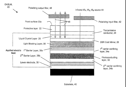
beneath the substrate 40 the substrate 40 itself is an electrical component in
the system.
Concentration of the arsenic precipitates (or other nodes acting as Schottky
barriers)
within the carrier confining layers 34a, 34b is determined by growth
procedures to support
high resolution of the device and sufficient trapping times for the electrons
e- and holes o+.
The thickness of the light blocking layer 30 may be relatively thin when using
any of
Indium gallium arsenide InGaAs, AlGaAs or GaAs for that layer 30, because they
have ,a
very high absorption coefficient. The molar concentration of indium or
aluminum in that
layer 30 is optimized for the particular distributed Bragg reflector DBR 28
with which it
functions in concert to form a filter.
[0052] Figure
4 more particularly details certain manufacturing efficiencies
that might be attained in making a OASLM 20 according to embodiments of the
invention.
At the top of Figure 4 are the lowermost eight layers described with reference
to Figure
I A, turned horizontal to match the time versus temperature growth profile
shown at the
lower portion of Figure 4. The substrate 40 is a GaAs wafer from which other
layers of
Figure 4 are grown. The temperature axis shows two temperatures, high and low,
which
in an embodiment represent 200-300 degrees C and 500-600 degrees C,
respectively.
Time for growing each layer depends on the layer thickness desired, and Figure
4 is not
intended to be proportional in the time axis.
[0053]
Temperature is raised to the higher temperature in region 50 to grow
the lower electrode 38 as a layer of highly doped GaAs, AlGaAs or InGaAs, the
latter two
materials grown in the presence of a vapor containing Al or In respectively.
The specific
concentration of the dopant, such as Si or Be, within the vapor is selected so
that the lower
electrode 38 is electrically conductive. The second barrier layer 36b may be
AlGaAs or
A1As, grown in region 52 at the higher temperature and is undoped so that the
second
CA 02644283 2008-08-29
WO 2007/103274 PCT/US2007/005531
barrier layer 36b is electrically insulating. Note that the arrangement of the
electrode and
barrier layers may be different as discussed above, specifically the electrode
may be
beneath the substrate and as such the barrier la'yer, if present at all, is
between the
electrode and the substrate.
=
[0054] Once the second barrier layer 36b is at or very near its
desired
thickness, temperature is lowered at region 54 as shown and the second carrier
confining
layer 34b is grown for example in one embodiment by Molecular Beam Epitaxy
(MBE).
As detailed above, upon annealing arsenic precipitates out from this layer
grown at a lower
growth temperature to form a layer of LTG-GaAs. Upon reaching the desired
thickness
for the second carrier confining layer 34b, the temperature is raised at
region 56 to grow
the photoconducting layer 32. While the undoped photoconducting layer 32 is
being
grown as GaAs or AlGaAs or InGaAs at the higher temperature, the second
carrier
confining layer 34b is being annealed as described above, and the arsenic
precipitates form
into spherical nodes that are nearly uniformly distributed throughout the
volume of the
second carrier confining layer 34b. Growth of the undoped photoconducting
layer 32
continues after the anneal of the second carrier confining layer 34b is
complete, as further
time may be necessary for the thicker photoconducting layer 32 of exemplary
embodiments of this invention. Further annealing the second carrier confining
layer 34b
. does not adversely impact its properties.
[0055] As the photoconducting layer 32 reaches its desired
thickness, the =
temperature is again dropped at region 58 to grow the first carrier confining
layer 34a
which upon annealing becomes LTG-GaAs, similar to the second carrier confining
layer
34b described above. Temperature is again raised at region 60 to grow the
first barrier
layer 36a as AlGaAs or AlAs such that the first barrier layer 36a is
electrically insulating.
That raised temperature at region 60 anneals the first carrier confining layer
34a.
Composition of the vapor in the MBE process is changed at region 62 to grow
the light
blocking layer 30 tuned to the specific parameters needed for its purpose, to
block visible
light as described above. As can be appreciated from the above, each layer
through at
least the first barrierlayer 36a may be grown sequentially in a continuous
process from the
substrate 40, which acts as seed layer. The different layers are grown by
varying certain
parameters within that continuous process, such as vapor composition, and
temperature,
but the process is unitary and continuous, so therefore highly efficient from
a
21
CA 02644283 2008-08-29
WO 2007/103274
PCT/US2007/005531
manufacturing perspective. This is seen as a distinct advantage over the prior
art,
especially prior art rear-addressed light valves which require the very
limiting constraint
that the substrate be transmissive. Light valves made by the process detailed
above are
. characterized in that the various layers formed from the same GaAs
(or other substrate)
cpitaxy exhibit a lattice structure that is not discontinuous among the
adjacent layers. For
example, while a GaAs photoconducting layer 32 may differ in molecular
structure from
an adjacent LTG-GaAs carrier confining layer, the lattice structures of these
distinct layers
flow continuously one into the other. This is because those layers are grown
in a single
epitaxial growth process of materials of like lattice, though in order to
define the distinct
layers that process may vary by temperature, pressure, molar concentration of
gas in the
surrounding environment, etc. As detailed above, a non-discontinuous lattice
structure
may be evident from the substrate 40 to the light blocking layer 30 and all
intervening
layers, or from the substrate 40 to any of those intervening layers.
(0056j The
DBR layer 28 may be considered a band pass or notch filter,
passing only wavelengths within a certain band or energy range and
substantially
reflecting all energy/wavelengths above and below that band. As above, the
light locking
layer 30 is tuned to block specifically those wavelengths outside the
wavelength-defined
notch. As such, the pass band through the DBR layer 28 may be limited in both
upper and
lower wavelength ranges.
(0057j
Figure 5 illustrates one embodiment of a light engine 64 that uses an
embodiment of an optically addressed spatial light modulator OASLM 20 such as
that of
Figure IA or the alternative embodiments detailed above. This particular
embodiment
uses a single OASLM 20 that processes visible light in three 'colors', where a
distinct IR
band of light addresses all three colors of visible light. A source 66 first
provides
addressing light in a single IR band that is focused at an addressing lens 68
and is reflected
by a first dichroic mirror 70 to reach the broadband PBS 72. In an embodiment,
the optics
cause the addressing light to be S-polarized (or P-polarized) once it passes
through the
addressing lens 68. In another embodiment, the source 66 itself provides
polarized
addressing light.
(0058] '
The addressing light then passes into a broadband polarizing
beamsplitter PBS cube 72 (or other shaped PBS component). Broadband PBS cubes
are
. 22
CA 02644283 2012-05-02
commercially available from the OptoSigma Corporation of Santa Ana,
California, and
various other manufacturers. The IR band addressing light is then reflected by
the PBS 74
toward a front face 22a of the OASLM 20. As detailed above, the addressing
light is
converted to art image in layer 26 upon application of a variable applied
electric field that
reverses over a period less than a capture time defined by the first carrier
confining layer
34a.
[00591 Read light in the visible range is emitted from the source 67
(or
from the same source as the IR addressing light source). In the embodiment of
Figure 5,
the read light is white light encompassing the entire visible spectrum. The
read light
passes through optics and is polarized and then passes through the first
dichroic mirror 70,
and into the PBS cube 72 to be reflected by the PBS 74 toward the front face
22a of the
OASLM 20. In the OASLM 20, the read light passes to the birefringent layer 26
where it
is modulated, and is reflected by the DBR layer 28 (and somewhat by the light
blocking
layer 30) to pass out of the OASLM 20 at the front face 22a. The modulated
read light
then passes back into the PBS cube 72, through the polarizer 74, and through
each of three
separate color filters 76. Light which does not pass through the polarizer 74
is reflected
back toward the source 67. Note that on the first pass toward the OASLM 20,
the read
light is reflected at the polarizer 74 but passes through it on the second or
'return' pass
after the OASLM 20. This is because layer 26 (shown in Figure IA) changes the
polarization state of the read light passing therethrough. The change in
polarization causes
the light to pass the polarizer 74 on the second pass. The polarization of the
read light on
the first pass may be set by the optics, or by a separate polarizing filter
(e.g., component
46 of Figure IA). The color filters 76 manage the visible read light emanating
from the
OASLM 20, which then passes through a series of projection lenses 78 which
throw the
image onto a screen, such as a glass surface of a rear projection TV or a wall
(or unrolled
screen) if the light engine is part of a stand-alone projector that does not
include an
intrinsic projection screen. Figure 5 is seen as a lower cost embodiment as
compared to
Figures 6-7, since of those embodiments only Figure 5 uses a single OASLM 20.
[0060] Figure 6 illustrates an embodiment of a light engine 80 that
uses
three distinct-color light valves 20-R, 20-G, and 20-B (for red, green and
blue,
respectively) about a PBS/x-cube arrangement. The addressing light source 66,
addressing
lens 68, first dichroic mirror 70, PBS cube 72, and second polarizer 74 are
similar in
23
=
CA 02644283 2008-08-29
WO 2007/103274
PCT/US2007/005531
principal to those same components described with respect to Figure 5, except
that in
Figure 6, the addressing light is shown in three distinct IR bands. These IR
addressing
light bands may emanate from a single source 66 or from multiple sources, as
those IR
addressing light bands are divided by the dichroic x-cube 82, of which an
exemplary
embodiment is also available from the OptoSigma Corporation of Santa Ana,
California.
The source 66 may provide addressing light and read light, or read light may
be provided
by a separate source 67. In either instance, the addressing light passes
through the
addressing lens 68 in order to be properly imaged on the OASLM 20.
[0061]
Specifically, as compared to the embodiment of Figure 5, the
embodiment of Figure 6 disposes a dichroic x-cube 82 between the PBS 72 and
the
OASLM 20, and rather than a single OASLM 20, one color-specific OASLM 20-R, 20-
G,
20-B is disposed adjacent to each of the remaining sides of the dichroic x-
cube not
adjacent to the PBS 72. Within the x-cube 82 are first and second cross-
dichroic mirrors
84 and 86, respectively. The reflectance and pass characteristics of the first
and second
cross-dichroic mirrors 84, 86 are such that the first cross-dichroic mirror 84
passes IRR
addressing light of S-polarization, reflects IRB addressing light of S-
polarization, and
passes red read (visible) light of both S and P polarization but reflects blue
read (visible)
light of either polarization. The second cross-dichroic mirror 86 passes IRB
addressing
light of S-polarization reflects IRR addressing light of S-polarization, and
passes blue read
(visible) light of both S and P polarization but reflects red read (visible)
light of either
polarization. Both the first and second cross-dichroic mirrors 84, 86 also
pass IRG
addressing light of S-polarization and pass green read (visible) light of both
S and P
polarizations. Of course, the above assumes that the initial polarization of
light into the
PBS 72 is S-polarized; the polarizations above are reversed if the initial
polarization is P
with the read light switched to S-polarization within the various light valves
20-R, 20-G,
and 20-B.
[0062] The end
result is shown in Figure 6: addressing light of the IRR
band is essentially passed only to the OASLM 20-R that is sensitive to (tuned
to) that band
of addressing light. The DBR layer 28 and light blocking layer .30 of that
particular
OASLM 20-R are designed to block light outside the IRR range, including
visible light,
IRG and IRB. When read light in the visible red band and of a first
polarization (e.g., S)
passes through the x-cube 82, it is reflected from the second dichroic mirror
86 and passes
24
CA 02644283 2008-08-29
WO 2007/103274
PCT/US2007/005531
through the first dichroic mirror 84 to enter the red-tuned OASLM 20-R. That
read light,
in the red visible band, is changed in polarization state to .a second
polarization state
within the OASLM 20-R, exits into the x-cube 82, is reflected from the second
cross
dichroic mirror 86 and passes through the first cross-dichroic mirror 84, and
continues in a
second pass through the polarizer 74 of the PBS 72 and out toward the
projecting lenses
78 (that red light that does not pass through the polarizer 74 is reflected by
it and
eventually trapped at the source 67). The remaining two light valves 20-G and
20-B =
operate similarly, with the various cross-dichroic filters 84, 86 and
polarizations operating
to selectively pass and reflect light within the appropriate write and read
bands into and
out of the select light valve.
[0063] Figure
7 is an illustration of a particularly advantageous light engine
88 using three color-distinct light valves 20-R, 20-G, 20-B about two
different PBS cubes
72', 72" and an integrating PBS cube 90. The embodiment of Figure 7 represents
an
adaptation of a prior art optical engine, commonly termed "Colorlink
technology" or
similar, to forward addressed OASLMs 20-R, 20-G, 20B according to embodiments
of this
invention. A source 66, addressing lens 68, and projection lens 78 are similar
to those
described with reference to Figure 5. IR addressing light in three IR bands
emanates from
a singular source or multiple sources 66 (that may be contemporaneous with 67)
that may
be polarizing with the IR light passing through an addressing lens. Visible
read light
emanates from a singular source or multiple sources 67. One or more polarizing
filters
may be disposed along the illustrated optical pathways so that the IRR is
polarized
differently than the IRG and IR B addressing light. In this description, IR R
is P-polarized
and IRG and IRB are each S-polarized, but those conventions may be readily
reversed.
Alternatively but not specifically illustrated, the different wavelength bands
of addressing
light entering from the left of Figure 7 may all exhibit the same polarization
state, and a
dichroic filter may be disposed in front of the polarizer 96 to enable this or
the Colorlink0
filters can be modified accordingly. In other embodiments, there need be no
polarization
of the different addressing light streams. A hot mirror 92 directs all IR and
visible light
within the bands of interest to a blue-transmitting dichroic mirror 94. The
positions of 20-
R, 20-G, 20-B can be varied and as such the descriptions of the light paths
will vary
accordingly; the specific disposition shown in Figure 7 is illustrative and
exemplary, not
exhaustive.
CA 02644283 2008-08-29
WO 2007/103274
PCT/US2007/005531
[0064] IR
addressing light IR0 corresponding to visible blue read light
passes through dichroic mirror 94 toward a blue-oriented polarizer 72' and
reflects off of
polarizer 98 of PBS 72' to enter the blue-tuned OASLM 20-B. Read light in the
visible
blue range passes the .same optical pathway, where portions may be changed to
P-
polarization within the OASLM 20-B, and passes out of the OASLM 20-B, through
the
blue-oriented PBS 72' and into the integrating PBS cube 90. Similarly, IR
addressing
light IRG and IRR corresponding to visible green and red read light
(respectively) is
reflected from the blue-transmitting dichroic mirror 94 and passes into a red
and green-
oriented PBS 72". Within that PBS 72", the IRR addressing light passes an
IRR/IRG
oriented dichroic mirror in front of the polarizer of 96 and enters a red-
tuned OASLM 20-
R. Read light in the visible red range passes the same optical pathway as
described for
IRR, is changed to P-polarization within the OASLM 20-R to pass out of the
OASLM 20-
R, and is reflected by the red/green-oriented dichroic mirror 96 toward the
integrating PBS
cube 90. Within that same PBS 72", the IRG addressing light is reflected from
the
red/green oriented dichroic mirror 96 and enters a green-tuned OASLM 20-G.
Read light
in the visible green range passes the same optical pathway as described for
IRG, is changed
to P-polarization within the OASLM 20-G to pass out of the OASLM 20-R, and
passes
through the red/green-oriented dichroic mirror 96 toward the integrating PBS
cube 90.
[0065] At this
point, all three of the read light colors, red, green and blue,
are present within the integrating PBS 90. Blue is reflected from the
integrating PBS 99
while red and green pass through it, and all three colors as modulated by the
separate light
valves 20-R, 20-G and 20-B pass through the projection lens 78 together for a
multi-color
image projection. Advantages over prior-art Colorlink technology light
engines are as
follows.
[0066] For LED
illuminated read light, power and therefore heat are greatly
reduced in the embodiment of Figure 7. Whereas prior art Colorlink technology
uses
typically an arc lamp as shown in the block encircled by the dashed line (and
its associated
very high energy usage and heat generation). The embodiment of Figure 7 may
use an IR
laser diode, LED or other source along with a micro-electrical mechanical
system
(MEMS), or even a ferro-electric liquid crystal (FLC) device or nematic liquid
crystal
(NLC) device as the addressing light source 66 that operates on a scale of
about 50
microwatts per square centimeter of the OASLM 20. This addressing light
modification is
26
CA 02644283 2012-05-02
not present in LCoS implementations of the Colorlink technology. Heat
generation has
become such a concern in "current projector technology that consumers are
often given
average bulb time in order to compare and contrast different projectors,
including rear-
projection televisions.
[0067] Second,
Colorlink technology of the prior art imposes great
difficulty in aligning the three different color images prior to the
projection lens. The
embodiments of Figures 6 and 7 do not suffer from the need for a separate
alignment
regimen for the different images because they all derive fro. rn the same
addressing light
source yielding exact pixel alignment. Aligning the various color-specific
images is
merely a matter of equalizing the different optical paths between the source
66 and the
projection lens 78, a fairly straightforward process for which accuracies
beyond what is
sensible by the human eye are readily achieved.
[0068) Figure 8
illustrates another optical engine 100 configured for use with the
OASLM embodiments described above. A light source 102 such as an arc lamp or
LED
outputs to a series of two fly's eye lenses 104, 106 and a relay lens 108 and
is split at a
dichroic splitter or dichroic filter 110 into red, green and blue bands (shown
respectively
as R, G and B). The pathway of the red band will be detailed; those of the
blue and green
bands are similar in concept. The red band light is reflected by a pair of
turning mirrors or
turning dichroics 112, 114 through another relay lens 116 and through a
polarizer 118
disposed for convenience at a 45 degree angle to the optical pathway. By
example, the
polarizer 118 may be known as a wired grid polarizer (e.g., available from
Moxteke), a
thin film polarizer (e:g., available from McNeil ), or a polarizing beam
splitter (e.g., such
as a Viquiti splitter available from 3M0). The red band passes through
straight through
the polarizer 118 and into the OASLM 20 light valve such as those detailed at
Figures 1A-
C. Output light from that OASLM 20 reflects from the polarizer 118 toward one
input
side 120a of an X-cube 122, preferably through a clean-up polarizer 124. Green
and blue
bands follow similar pathways, with similar components for those pathways
labeled in
Figure 8 with a prime for blue and double prime for green (with the exception
of the
turning mirrors 112', 114', through which pass both blue and green bands).
Blue light
enters a second input side 120b of the X-cube 122, and green light enters a
third input side
120c of the X-cube 122. The red, blue and green bands are combined in the X-
cube 122
and pass through an output side 120d into output or projection optics
arrangement 126.
27
CA 02644283 2012-05-02
[00691 Also in Figure
8 is shown apparatus for addressing optics, termed above as
write light. A write light source 130 is shown as three LEDs, each outputting
infrared
write light in a different band for red, blue and green_ The infrared source
light passes
through a beam expander 132 and a polarizer 134 (or optionally a beam steerer
if polarized
light is not used) and into a write light modulator 136. Modulated write light
is output
from the modulator 136 and redirected at the polarizer 134 toward the dichroic
.splitter 110
previously detailed.
[00701 Although
described in the context of particular embodiments, it will
be apparent to those skilled in the art that a number of modifications and
various changes
to these teachings may occur. Thus, while the invention has been particularly
shown and
described with respect to one or more embodiments thereof, it will be
understood by those
skilled in the art that certain modifications or changes may be made therein
without
departing from the scope of the invention as set forth above, or from the
scope of the
ensuing claims, where the claims recite a layer disposed 'over' or 'under'
another layer,
that relation describes a relative disposition and is not to imply the layers
are necessarily
adjacent to one another; a layer being disposed over another layer does not
preclude one or
more intervening layers therebetween.
28