Note: Descriptions are shown in the official language in which they were submitted.
CA 02644493 2008-09-25
WO 2007/109883 PCT/CA2007/000478
NON-VOLATILE SEMICONDUCTOR MEMORY WITH PAGE ERASE
RELATED APPLICATIONS
This application claims the benefit of U.S. Provisional Application No.
60/786,897,
filed on March 29, 2006, U.S. Provisional Application No. 60/843,593, filed on
September
11, 2006 and U.S. Utility Application Serial No. 11/715,838, filed on March 8,
2007. The
entire teachings of the above applications are incorporated herein by
reference.
BACKGROUND OF THE INVENTION
Mobile electronic devices, such as digital cameras, portable digital
assistants, portable
audio/video players and mobile terminals continue to require mass storage
memory,
preferably non-volatile memory with ever increasing capacities and speed
capabilities. For
example, presently available audio players can have between 256Mbytes to 40
Gigabytes of
memory for storing audio/video data. Non-volatile memory such as Flash memory
and hard-
disk drives are preferred since data is retained in the absence of power.
Presently, hard disk drives having high densities can store 40 to 500
Gigabytes of
data, but are relatively bulky. However, Flash memory, also known as solid-
state drive, is
popular because of their high density, non-volatility, and small size relative
to hard disk
drives. Flash memory technology is based on EPROM and EEPROM technologies. The
term "flash" was chosen because a large number of memory cells could be erased
at one time
as distinguished from EEPROMs, where each byte was erased individually. Those
of skill in
the art will understand that Flash memory can be configured as NOR, NAND or
other Flash,
with NAND Flash having higher density per given area due to its more compact
memory
array structure. For the purpose of further discussion, references to Flash
memory should be
understood as being any type Flash memory.
The cell array structure of NAND flash memory consists of n erasable blocks.
Each
block is subdivided into m programmable pages illustrates the cell array
structure of an
example NAND flash memory which consists of n erasable blocks. In this
example, n=2048.
Each block is subdivided into m programmable pages as shown in Figs 1 to 3,
where m=64.
CA 02644493 2008-09-25
WO 2007/109883 PCT/CA2007/000478
Each page consists of (j+k) bytes (x8b) as shown in Figure 3. In this example,
j=2048
and k=64. The pages are further divided into a j-byte data storage region
(data field) with a
separate k-byte area (spare field). The k-byte area is typically used for
error management
functions.
= 1 page =(j + k) bytes.
= 1 block = m pages =(j + K) bytes * m.
= Total memory array size = n blocks =(j + K) bytes * m * n.
In conventional NAND flash devices, read and program operations are executed
on a
page basis while erase operations are executed on a block basis. All
operations are driven by
commands (refer to Samsung's 2Gb NAND Flash Specification: ds k9flgxxu0m rev10
incorporated herein in its entirety).
The internal memory array is accessed on a page basis. The read operation
starts after
writing READ command followed by addresses via common UO pins (1/00 to UO 7)
to the
device. The 2,112 bytes of data within the selected page are sensed and
transferred to the
page register in less than tR (data transfer time from flash array to page
register) shown in
Figure 4. Once the 2,112 bytes of data are sensed and transferred from the
selected page in
the cell array to the data register, the data in the data register can be
sequentially read from
the device at, for example, 8 bits or 16 bits per cycle.
The conventional memory array is programmed on a page basis. For program
operations, PROGRAM command followed by addresses and input data of 2,112
bytes is
issued to the device through common UO pins (1/00 to U07). The 2,112 bytes of
data are
transferred to the data register during input data loading cycles and finally
programmed to the
selected page of the cell array less than tPROG (page program time) as shown
in Figure 5.
The memory array is erased on a block basis. For block erase operations, BLOCK
ERASE command followed by block addresses is issued to the device through
common UO
pins (1/00 to U07). The 128K bytes of data are erased less than tBERS (block
erase time) as
shown in Figure 6. Refer to NAND Flash specifications (Samsung's 2Gb NAND:
ds_k9f2gxxu0m_rev10) for detailed device operations.
A NAND cell string typically consists of one string selector transistor 71, i
memory
cells 72 and one ground select transistor 73 which are serially connected as
shown Figure 7.
The number (i) of cells per string can be varied by process technology, for
example 8 cells
-2-
CA 02644493 2008-09-25
WO 2007/109883 PCT/CA2007/000478
per string or 16 cells per string or 32 cells per string. 32 memory cells per
string are common
in present 90nm and 70nm technologies. Hereinafter, `32' is used for i as
shown in Fig. 7.
Memory cell gates correspond to wordline 0 to 31 (W/L0 to W/L 31). The gate of
string select transistor is connected to a string select line (SSL) while the
drain of string select
transistor is connected to bitline (B/L). The gate of ground select transistor
is connected to a
ground select line (GSL) while the source of ground select transistor is
connected to common
source line (CSL). Each wordline corresponds to a page and each string
corresponds to a
block.
Figure 8 and 9 depict physical structure of a block with 32 cells per NAND
cell string.
As shown in Fig. 8, there are (j +k)*8 NAND strings in a block. Thus the unit
block has total
(j + k)*8*32 cells. Each wordline is defined as unit page. Fig. 9 shows n
blocks
Typically, flash memory cells are programmed and erased by either Fowler-
Nordheim
(F-N) tunneling or hot electron injection. In NAND flash memory, both erase
and program
are governed by F-N tunneling. The following erase and program operations are
based on
NAND flash memory.
During an erase operation, the top poly (i.e. top gate) of the cell is biased
to Vss
(ground) while the substrate of the cell is biased to erase voltage Vers (eg.
approximately
20v, source and drain are automatically biased to Vers due to junction-
forward-bias from P-
substrate to n+ source/drain). By this erase bias condition, trapped electrons
(charge) in the
floating poly (i.e. floating gate) are emitted to the substrate through the
tunnel oxide as shown
in Figure 10A. The cell Vth of the erased cell is negative value as shown in
Figure l OB. In
other words, the erased cell is on-transistor (normally turn-on with gate bias
Vg of OV).
During a program operation, on the contrary, the top poly (i.e. top gate) of
the cell is
biased to program voltage Vpgm (eg. approximately 18v) while the substrate,
source and
drain of the cell are biased to Vss (ground). By this program bias condition,
electrons
(charge) in the substrate are injected to the floating poly (i.e. floating
gate) through the tunnel
oxide as shown in Figure 11A. The cell Vth of the programmed cell is positive
value as
shown in Figure 11 B. In other words, the programmed cell is off-transistor
(normally turn-
off with gate bias Vg of OV).
Therefore NAND flash is erased and programmed by a bi-directional (i.e.
symmetrical) F-N tunneling mechanism.
-3-
CA 02644493 2008-09-25
WO 2007/109883 PCT/CA2007/000478
One known erase scheme is illustrated in Figs. 12 and 13. Figure 12 shows bias
condition during erase operations. The p-well substrate is biased to erase
voltage Vers while
bitlines and the common source line (CSL) in the selected block are clamped to
Vers-0.6v
through the S/D diodes of the SSL and GSL transistors. At the same time all
wordlines in the
selected block are biased to OV while the string select line (SSL) and the
ground select line
(GSL) are biased to erase voltage Vers. Therefore entire cells in the selected
block are erased
by F-N tunneling as described above.
Because of block basis erase operations, erasure of memory cells in unselected
blocks
having the same p-well substrate must be prevented (i.e. erase inhibit).
Figure 13 shows an
erase inhibit scheme to unselected blocks:
= All wordlines in the selected block are biased to OV.
= All wordlines in unselected blocks are biased to Vers to compensate
electrical
field by Vers from the substrate.
Table 1 shows bias conditions for the selected block and unselected blocks
with the
prior art 1 during erase operations.
Table 1. Bias Conditions during Erase - Prior Art 1
SELECTED BLOCK UNSELECTED BLOCK
BITLINES (B/L) CLAMPED TO Vers- CLAMPED TO Vers-0.6V
0.6V
STRING SELECT Vers Vers
LINE (SSL)
WORDLINES (W/L0 OV Vers
- W/L3 1)
GROUND SELECT Vers Vers
LINE (GSL)
COMMON SOURCE CLAMPED TO Vers- CLAMPED TO Vers-0.6V
LINE (CSL) 0.6V
SUBSTRATE Vers Vers
(POCKET P-WELL)
-4-
CA 02644493 2008-09-25
WO 2007/109883 PCT/CA2007/000478
With this erase inhibit scheme, it takes a very long total erase time to
charge all
wordlines in unselected blocks to erase voltage Vers. At the same time, the
power
consumption is very high due to charging and discharging entire wordlines in
unselected
blocks. Moreover, as the memory density increases, the erase time becomes much
longer and
the power consumption during erase operations is much higher.
In order to resolve problems in the above approach, the self-boosting erase
inhibit
scheme (US Patent # 5,473,563) has been proposed and it is widely used in NAND
flash
memories.
For the selected block, the erase bias conditions are substantially the same
as above
except the SSL and GSL are floating instead of biased to Vers, as shown in
Figure 14.
To prevent erasure of memory cells in unselected blocks, all wordlines in
unselected
blocks are floated during erase operations as shown in Fig. 15. Therefore
floated wordlines
in unselected blocks are boosted to nearly erase voltage Vers by capacitive
coupling between
the substrate and wordlines in unselected blocks as applying erase voltage
Vers to the
substrate. (Floated wordlines are boosted to about 90% of Vers when the
substrate of the cell
array goes to Vers; however, boosted voltage level on floated wordlines is
determined by
coupling ratio between the substrate and wordlines.) The boosted voltage on
wordlines in
unselected blocks reduces electric field between the substrate and wordlines;
as a result,
erasure of memory cells in unselected blocks is prevented.
= All wordlines in the selected block are biased to OV.
= All wordlines in unselected blocks are floating.
Table 2 shows bias conditions during erase with this approach. There is no
need to
apply erase voltage Vers to wordlines in unselected blocks, which reduces
power
consumption during erase and reduces the erase time, because entire wordlines
in unselected
blocks are not needed to be biased to Vers.
Table 2. Bias Conditions during Erase - Prior Art 2
SELECTED BLOCK UNSELECTED BLOCK
BITLINES (B/L) CLAMPED TO Vers-0.6V CLAMPED TO Vers-0.6V
STRING SELECT BOOSTED TO APPROX. BOOSTED TO APPROX.
LINE (SSL) 90% OF Vers 90% OF Vers
-5-
CA 02644493 2008-09-25
WO 2007/109883 PCT/CA2007/000478
WORDLINES (W/L0 - OV BOOSTED TO APPROX.
W/L31) 90% OF Vers
GROUND SELECT BOOSTED TO APPROX. BOOSTED TO APPROX.
LINE (GSL) 90% OF Vers 90% OF Vers
COMMON SOURCE CLAMPED TO Vers-0.6V CLAMPED TO Vers-0.6V
LINE (CSL)
SUBSTRATE Vers Vers
(POCKET P-WELL)
Because the substrate of cells is biased to erase voltage Vers and
source/drain/substrate of cells in the selected block are electrically
connected, the erase
operation must occur on a block basis. In other words, the minimum erasable
array size is a
block.
The above described Flash memories suffer from three limitations. First, bits
can be
programmed only after erasing a target memory array. Second, each cell can
only sustain a
limited number of erasures, after which it can no longer reliably store data.
In other words,
there is a limitation in the number of erase and program cycles to cells (i.e.
Endurance,
typically 10,000-100,000 cycles). Third, the minimum erasable array size is
much bigger
than the minimum programmable array size. Due to these limitations,
sophisticated data
structures and algorithms are required to effectively use flash memories. (See
for example,
US Patents 5,937,425, 6732,221 and 6,594,183.
Erase of memory cells on a page basis has been suggested in U.S. Patent
5,995,417
and in patent application US 2006/0050594.
SUMMARY OF THE INVENTION
Provided here are technical details in new page basis erase approaches in
nonvolatile
memory, with particular application NAND flash memory. The page basis erase
approach is
described using NAND flash memory, but may be applied more generally by one
skilled in
the art to other flash memory devices.
A nonvolatile memory array, such as a NAND Flash Memory, has plural strings of
memory cells on a substrate, wordlines across the strings to pages of memory
cells and a pass
transistor applying a voltage to each wordline. In a method of erasing a page,
each pass
-6-
CA 02644493 2008-09-25
WO 2007/109883 PCT/CA2007/000478
transistor of a selected block is enabled, for example through a block
decoder. A wordline
decoder may cause a select voltage to be applied to the pass transistor at
each of plural
selected wordlines of the selected block and an unselect voltage to be applied
to the pass
transistor at each of plural unselected wordlines of the selected block. A
substrate voltage is
applied to the substrate of the selected block. The voltage difference between
the substrate
voltage and a resulting voltage of each selected wordline causes the page of
memory cells of
the selected wordline to erase, and the voltage difference between the
substrate voltage and
the resulting voltage of each unselected wordline is less than that which
erases the page of
memory cells of the unselected wordline.
In certain embodiments, a common select voltage is applied at each selected
wordline
and a common unselect voltage is applied at each unselected wordline. Select
voltages and
unselect voltages may be applied to any of the wordlines of a selected block.
With the application of select and unselect voltages to any of the wordlines
of a
selected block, selected wordlines may be separated by at least one unselected
wordline and
unselected wordlines may be separated by at least one selected wordline. With
selected lines
adjacent to unselected lines, where boosting of a wordline is relied upon, the
capacitive
coupling that results in that boosting can be reduced. As a result, a higher
initial voltage
applied from the unselect voltage is preferred. To assure that unselected
memory cells
adjacent to two selected memory cells are not erased, it is preferred that the
unselect voltage
be closer to the applied substrate voltage than to the select voltage.
In one embodiment, the resulting voltage of each selected wordline is
substantially the
same as the select voltage and the resulting voltage of each unselected
wordline is a floating
voltage pulled from the unselect voltage toward the substrate voltage. A
common gate signal
applied to each pass transistor of the selected block has a value V2, the
unselect voltage is
great than V2 and the unselected wordline precharges to V2-Vtn. V2 is
substantially less
than the applied substrate voltage but is preferably at least 50% of the
applied substrate
voltage. As such, the unselect voltage in a selected block is greater than the
voltage typically
applied to the pass transistors in an unselected block.
In other embodiments, the resultant voltage of each selected wordline is
substantially
the same as the select voltage and the resulting voltage of each unselected
wordline is
substantially the same as the unselect voltage. For example, the select
voltage may be about
OV and the unselect voltage may be about equal to the applied substrate
voltage.
-7-
CA 02644493 2008-09-25
WO 2007/109883 PCT/CA2007/000478
In an erase verify operation, a select verify voltage may be applied to each
wordline
of plural erased pages in the selected block and an unselect verify voltage
may be applied to
each wordline of plural nonerased pages in the selected block. The state of
strings of the
selected block is then sensed. Each string is connected to an end voltage,
specifically a
source voltage. The level of the end voltage may be selected from one of
plural voltage
levels dependent on the number of selected wordlines.
BRIEF DESCRIPTION OF THE DRAWINGS
The foregoing will be apparent from the following more particular description
of
example embodiments of the invention, as illustrated in the accompanying
drawings in which
like reference characters refer to the same parts throughout the different
views. The drawings
are not necessarily to scale, emphasis instead being placed upon illustrating
embodiments of
the present invention.
Figure 1. NAND Flash Cell Array Structure.
Figure 2. NAND Flash Block Structure.
Figure 3. NAND Flash Page Structure.
Figure 4. Page Basis Read Operation in NAND Flash.
Figure 5. Page Basis Program Operation in NAND Flash.
Figure 6. Block Basis Erase Operation in NAND Flash.
Figure 7. NAND Cell String with 32 cells.
Figure 8. Block and Page Definition in NAND Flash.
Figure 9. Multiple Block in NAND Flash.
Figure I OA. Erase Operation by Fowler-Nordheim (F-N) Tunneling.
Figure l OB. Erase Operation by Fowler-Nordheim (F-N) Tunneling.
Figure I IA. Program Operation by Fowler-Nordheim (F-N) Tunneling.
Figure 11B. Program Operation by Fowler-Nordheim (F-N) Tunneling.
Figure 12. Bias Conditions to Selected Block during Erase - Prior Art I.
Figure 13. Block Erase and Static Erase Inhibit Scheme - Prior Art 1.
Figure 14. Bias Conditions to Selected Block during Erase - Prior Art 2.
Figure 15. Block Erase and Self-boosting Erase Inhibit Scheme - Prior Art 2.
Figure 16. Block Copy Process to Modify a Page or a Portion of the Page.
Figure 17. Bias Conditions to Selected Block during Erase - Page Erase.
Scheme 1
-8-
CA 02644493 2008-09-25
WO 2007/109883 PCT/CA2007/000478
Figure 18. Page Erase and Erase Inhibit - Page Erase Scheme 1.
Figure 19. Page Erase Bias Conditions - Page Erase Scheme 2A.
Figure 20. Page Erase and Erase Inhibit - Page Erase Scheme 2A.
Figure 21. Page Erase Bias Conditions - Page Erase Scheme 2B.
Figure 22. Page Erase and Erase Inhibit - Page Erase Scheme 2B.
Figure 23. Multiple Pages Erase - Page Erase Scheme 1.
Figure 24. Multiple Pages Erase - Page Erase Scheme 2A.
Figure 25. Multiple Pages Erase - Page Erase Scheme 2B.
Figure 26. Block Erase - Page Erase Scheme 2A.
Figure 27. Block Erase - Page Erase Scheme 2B.
Figure 28. Page Erase Verify without Source Bias.
Figure 29. Page Erase Verify with Source Bias.
Figure 30. Block Erase Verify.
Figure 31. Page Erase Flow - Single Erase & Erase Verify Cycle.
Figure 32. Page Erase Flow - Multiple Erase & Erase Verify Cycle.
Figure 33. Simplified Block Diagram of NAND Flash Core.
Figure 34. Block Decoder Schematic for Page Erase Scheme 1.
Figure 35. Block Decoder Schematic for Page Erase Scheme 2A and 2B.
Figure 36. Page Buffer and Column Selector - Example.
Figure 37. Page Erase/Multiple Page Erase Timing - Page Erase Scheme 1.
Figure 38. Page Erase/Multiple Page Erase Timing - Page Erase Scheme 2A.
Figure 39. Page Erase/Multiple Page Erase Timing - Page Erase Scheme 2B.
Figure 40. Block Erase Timing - Page Erase Scheme 2A.
Figure 41. Block Erase Timing - Page Erase Scheme 2B.
Figure 42. Page Erase Verify Timing for Page Erase Scheme 1 with Source Bias.
Figure 43. Block Erase Verify Timing for Page Erase Scheme 1.
Figure 44. Page Erase Verify Timing for Page Erase Scheme 2A and 2B.
Figure 45. Block Erase Verify Timing for Page Erase Scheme 2A and 2B.
Figure 46. Bias Conditions to Selected Block during Erase - Page Erase
Scheme 3.
Figure 47. Bias Conditions to Selected Block during Erase - Page Erase
Scheme 3.
-9-
CA 02644493 2008-09-25
WO 2007/109883 PCT/CA2007/000478
Figure 48. Page Erase and Erase Inhibit - Page Erase Scheme 3.
Figure 49. Multiple Page Erase and Erase Inhibit - Page Erase Scheme 3.
Figure 50. Parasitic capacitance during Page Erase Scheme 3.
Figure 51. Page Erase/Multiple Page Erase Timing - Page Erase Scheme 3.
DETAILED DESCRIPTION OF THE INVENTION
A description of example embodiments of the invention follows.
The teachings of all patents, published applications and references cited
herein are
incorporated by reference in their entirety.
In flash memory, especially NAND flash devices, read and program operations
are
executed on a page basis while erase operations are executed on a block basis.
Typically the
page size is 512 bytes, 2048 bytes, or 4096 byte while the block size is 16
pages, 32 pages, or
64 pages. Therefore the minimum erasable block size is at least 16 times
larger than the page
size. Moreover, this minimum size of erasable block (i.e. unit erase block) is
getting bigger
as the chip size increases.
The array size mismatch between program/read and erase introduces two critical
problems in device reliability (i.e. device lifetime) and system performance
degradation in
flash file system.
Unlike hard disk (HDD), memory cells in flash memory devices must be erased
before being programmed by input data. Data write operations should be
immediately
executed once the CPU or flash controller in the system issues the program
command. Thus
the erase-before-program decreases overall system performance. In order to
overcome this
problem, the flash controller typically prepares empty erased blocks in
advance (i.e. Erase-
unit Reclamation). This reclamation can take place either in the background
(when the CPU
is idle) or on-demand when the amount of free space drops below a
predetermined threshold.
When the flash controller requests data write or data modification even into a
small
portion of the page, typically the block containing a page to be modified will
be rewritten to
one of free (empty) blocks declared by the erase-unit reclamation. In this
case, valid pages
containing original data in the original block should be copied to the
selected free block as
shown in Figure 16. The modified page is read, modified and copied to the new
block then,
the new block having modified data in a page with original data in the rest of
pages is
remapped to the valid block address by a virtual mapping system in the flash
controller. (The
virtual mapping system is an address translation system between logical
addresses accessed
-1.0-
CA 02644493 2008-09-25
WO 2007/109883 PCT/CA2007/000478
by the flash controller and physical addresses in the flash memory.) The
original block is
now obsolete and will be declared as a free block by the erase-unit
reclamation process.
(Refer Eran Gal, Sivan Toledo, "Algorithms and Data Structures for Flash
Memories," ACM
Computing Surveys, Vol. 37, No. 2, pp. 138-163, Jun. 2005, incorporated herein
by reference
in its entirety for algorithms and data structures for flash memories.) To
minimize
performance degradation due to the block copy operation described above
generally NAND
flash devices support a page copy function without external transaction
between flash devices
and the flash controller. Nevertheless, the array size mismatch between
program/read and
erase operations introduces a huge system overhead and complexity.
The flash memory cell is programmed and erased by either Fowler-Nordheim
tunneling or hot electron injection. During a program or erase operation,
charge is transferred
to or from a floating gate through the dielectric surrounding the floating
gate. This frequent
charge transfer causes electrons to be trapped in the floating gate and the
dielectric, which
degrades program and erase characteristics of cells. Consequent cells require
gradually higher
program voltage and erase voltage due to this electron trapping with an
increasing number of
erase-program cycles; as a result, the number of erase-program cycles on a
cell is limited.
Typically the maximum number of erase-program cycle (i.e. cell endurance
characteristic) is
between 10,000 and 100,000.
The limited number of erase-program cycles (endurance) limits the lifetime of
a flash
device. It would be advantageous to have a lifetime that is as long as
possible, and this
depends on the pattern of access to the flash device. Repeated and frequent
rewrites to a
single cell or small number of cells will bring the onset of failures soon and
end the useful
lifetime of the device quickly
Moreover, in the flash memory system having multiple flash devices, if there
is
significantly uneven use among devices in the flash memory system, one device
reaches an
end of lifetime while other devices have significant life left in them. When
the one device
reaches an end of lifetime, the entire memory system may have to be replaced,
and this
greatly reduces the life time of the flash memory system.
If rewrites can be evenly distributed to all cells of the device, each cell
will experience
close to the maximum number of erases it can endure, and so the onset of
failures will be
delayed as much as possible, maximizing the lifetime of the device. To extend
the device
-11-
CA 02644493 2008-09-25
WO 2007/109883 PCT/CA2007/000478
lifetime by even use across all the cells of the device, many wear-leveling
techniques and
algorithms have been proposed and implemented in the flash memory system
The block copy operations due to the array size mismatch between read/program
and
erase described in the previous section introduces unnecessary rewrites
because unaffected
data in pages of the block should be rewritten (copied) to the new block with
modified data.
Thus it can dramatically extend the device lifetime if the minimum erasable
array size is a
page (i.e. page basis erase) instead of a block (i.e. block basis erase)
because only pages to be
rewritten need to be erased. In addition, the number of block copy operation
will be greatly
reduced by the page basis erase.
Each NAND cell string in the NAND flash memory can be controlled independently
although the cell substrate is common across NAND cell strings of the device.
All wordlines
in a block during erase operations are biased to the same voltage condition in
typical NAND
flash devices. This is why the minimum erasable array size is a block in the
NAND flash
memory.
In order to erase flash memory cells in a page basis, each wordline
corresponding to a
page of the NAND cell string must be controlled separately and independently.
Page Erase Scheme 1
Table 3 and Figure 17 show bias conditions during page erase according to a
page
erase scheme 1(for example, erase of wordline 27). With the page erase scheme
1,
unselected wordlines are biased to a voltage for preventing the unselected
page(s) from being
erased, for example, Vers while the selected wordline(s) is(are) biased to
another voltage for
erasing the selected page(s), for example, OV.
As shown in Figure 17, within the selected block
= Selected wordline(s) in the selected block is(are) biased to OV for erase,
and
= Unselected wordline(s) in the selected block is(are) biased to Vers for
erase inhibit.
To prevent erasure of memory cells in unselected blocks, all wordlines in
unselected
blocks are floated during erase operations, which is the same as the prior art
2, while bias
conditions shown in Table 3 are applied to the selected block as shown in
Figure 18.
Therefore floated wordlines in unselected blocks are boosted to nearly erase
voltage Vers by
capacitive coupling between the substrate and wordlines in unselected blocks
as applying
erase voltage Vers to the substrate. (The wordlines are boosted to about 90%
of Vers when
the substrate of the cell array goes to Vers; however, boosted voltage level
on floated
-12-
CA 02644493 2008-09-25
WO 2007/109883 PCT/CA2007/000478
wordlines is determined by coupling ratio between the substrate and
wordlines.) The boosted
voltage on wordlines in unselected blocks reduces electric field between the
substrate and
wordlines; as a result, erasure of memory cells in unselected blocks is
prevented.
= All wordlines in unselected blocks are floating.
Table 3. Bias Conditions during Page Erase - Page Erase Scheme 1
SELECTED BLOCK UNSELECTED BLOCK
BITLINES (B/L) CLAMPED TO Vers-0.6V CLAMPED TO Vers-0.6V
STRING SELECT LINE BOOSTED TO APPROX. BOOSTED TO APPROX.
(SSL) 90% OF Vers 90% OF Vers
SELECTED OV BOOSTED TO APPROX.
WORDLINE 90% OF Vers
UNSELECTED Vers BOOSTED TO APPROX.
WORDLINE 90% OF Vers
GROUND SELECT BOOSTED TO APPROX. BOOSTED TO APPROX.
LINE (GSL) 90% OF Vers 90% OF Vers
COMMON SOURCE CLAMPED TO Vers-0.6V CLAMPED TO Vers-0.6V
LINE (CSL)
SUBSTRATE Vers Vers
(POCKET P-WELL)
Page Erase Schemes 2A and 2B
The bias condition for the page erase schemes 2A and 2B is as follows:
= Cell gate (wordline) is biased to negative voltage -V 1(first level
voltage).
= Cell substrate is biased to a second level voltage.
= Electric field between cell gate and substrate should meet a requirement to
incur F-
N tunneling through the tunnel oxide of the cell.
= Trapped electrons (charge) in the floating poly (i.e. floating gate) of the
cell are
emitted to the substrate through the tunnel oxide.
-13-
CA 02644493 2008-09-25
WO 2007/109883 PCT/CA2007/000478
= The maximum of the second level voltage with the cell gate voltage of OV
should
not introduce cell erase disturbance on unselected neighboring pages (e.g.
shifting
threshold voltage or soft-erase).
= -V1 and the second level voltage can be varied in accordance with process
technology and cell characteristics.
Figure 19 shows voltage bias condition with the page erase scheme 2A to
selected
page (wordline 27 in this example) in the selected block during erase
operation. The selected
wordline 27 (page) is biased to negative voltage -18V (-V1) while unselected
wordlines are
biased to OV. The substrate of the cell array is biased to OV (V2 = OV). Again
the voltages
can be varied in accordance with process technology and cell characteristic,
which will be
explained hereafter in conjunction with Figures 21 and 22 and Table 5. With
the new erase
condition, all cells of the selected page are erased while all cells of
unselected pages are not
erased due to no effective magnitude of electric field between the cell gate
and the substrate.
Table 4 and Figure 20 show bias conditions for the selected block and
unselected
blocks. All wordlines of unselected blocks are floating during erase; hence
the potential of all
wordlines remain at OV because the substrate is biased to OV and all wordlines
of unselected
blocks are discharged to OV before being floated for the erase.
-14-
CA 02644493 2008-09-25
WO 2007/109883 PCT/CA2007/000478
Table 4. Bias Condition during Erase - Page Erase Scheme 2A
SELECTED BLOCK UNSELECTED BLOCK
BITLINES (B/L) OV OV
STRING SELECT LINE OV FLOATING AT OV
(SSL)
SELECTED WORDLINES -18V (-V1) FLOATING AT OV
UNSELECTED OV FLOATING AT OV
WORDLINES
GROUND SELECT LINE OV FLOATING AT OV
(GSL)
COMMON SOURCE LINE OV OV
(CSL)
SUBSTRATE (P-WELL OV OV
OR POCKET P-WELL)
Figure 21 shows voltage bias condition with the page erase scheme 2B to a
selected
page (wordline 27 in this example) in the selected block during erase
operation. The selected
wordline 27 (page) is biased to negative voltage -13V (-V 1) while unselected
wordlines are
biased to OV. The substrate of the cell array is biased to 5V. Total electric
field between the
gate and the substrate of cells is the same as that of the first example.
Voltage to the substrate
should be determined not to introduce erase disturbance (i.e. soft-erase) to
cells on the
unselected wordlines (pages) in the same NAND cell string.
Table 5 and Figure 22 show bias conditions for the selected block and
unselected
blocks. All wordlines of unselected blocks are floating during erase
operations, all wordlines
of unselected blocks are boosted to nearly the substrate voltage by capacitive
coupling
between the substrate and wordlines in unselected blocks as applying voltage
to the substrate.
(The boosted voltage is about 90% of substrate voltage; however boosted
voltage level on
floated wordlines is determined by coupling ratio between the substrate and
wordlines) The
-15-
CA 02644493 2008-09-25
WO 2007/109883 PCT/CA2007/000478
boosted voltage on wordlines in unselected blocks reduces electric field
between the substrate
and wordlines; as a result, erasure of memory cells in unselected blocks is
prevented.
Table 5. Bias Conditions during Erase - Page Erase Scheme 2B
SELECTED BLOCK UNSELECTED BLOCK
BITLINES (B/L) CLAMPED TO CLAMPED TO
SUBSTRATE-0.6V SUBSTRATE-0.6V
STRING SELECT LINE BOOSTED TO APPROX. BOOSTED TO APPROX.
(SSL) 90% OF SUBSTRATE 90% OF SUBSTRATE
SELECTED WORDLINES -13V (-V1) BOOSTED TO APPROX.
90% OF SUBSTRATE
UNSELECTED OV BOOSTED TO APPROX.
WORDLINES 90% OF SUBSTRATE
GROUND SELECT LINE BOOSTED TO APPROX. BOOSTED TO APPROX.
(GSL) 90% OF SUBSTRATE 90% OF SUBSTRATE
COMMON SOURCE LINE CLAMPED TO CLAMPED TO
(CSL) SUBSTRATE-0.6V SUBSTRATE-0.6V
SUBSTRATE (POCKET P- 5V SUBSTRATE 5V SUBSTRATE
WELL)
Multiple Pages Erase and Block Erase
With the new page erase concept, multiple pages (wordlines) in the selected
block can
be erased. In fact, by selective control of the wordline voltages, any one or
more pages of a
selected block may be erased. Furthermore, entire pages of the selected block
can be also
erased, which is basically block erase.
Figure 23 shows three pages (wordline 1, 27, 29) in the selected block are
erased at
the same time using bias conditions of the page erase scheme 1.
Figure 24 shows three pages (wordline 1, 27, 29) in the selected block are
erased at
the same time using bias condition of the page erase scheme 2A.
-16-
CA 02644493 2008-09-25
WO 2007/109883 PCT/CA2007/000478
Figure 25 shows three pages (wordline 1, 27, 29) in the selected block are
erased at
the same time using bias condition of the page erase scheme 2B.
Figure 26 shows all pages in the selected block are erased at the same time
using bias
condition of the page erase scheme 2A, which is the block erase.
Figure 27 shows all pages in the selected block are erased at the same time
using bias
condition of the page erase scheme 2B, which is the block erase.
Erase Verify
After erasing a single page or multiple pages or all pages in the selected
block, the
erase verify must be performed to guarantee that erased cells have proper
threshold voltage
margin to be read. This erase verify is performed by page buffers described
below. Figure
28, Figure 29, Figure 30, and Table 6 show voltage bias conditions during page
erase verify
and block erase verify. For multiple page verify, each selected page maybe
verified
consecutively (sequentially) after erase, but in a preferred approach, all are
verified at once.
Voltage numbers (i.e. Vread, Versvf, Vcslevf and Vbersvf) in Table 6 can be
varied in
accordance with process technology and cell characteristic.
Fig. 28 shows single page erase verify without source bias, Fig. 29 shows
single page
erase verify with source bias from CSL. Fig. 30 shows block erase verify.
-17-
CA 02644493 2008-09-25
WO 2007/109883 PCT/CA2007/000478
Table 6. Bias Condition during Erase Verify
PAGE ERASE PAGE ERASE BLOCK ERASE
VERIFY WITH VERIFY VERIFY
SOURCE BIAS WITHOUT
SOURCE BIAS
BITLINES (B/L) PRECHARGED PRECHARGED PRECHARGED
AND SENSED AND SENSED AND SENSED
STRING SELECT LINE Vread (4 - 5V) Vread (4 - 5V) Vread (4 - 5V)
(SSL)
SELECTED OV OR VersvF Versvf (- -1.5V) OV OR Vbersvf
WORDLINES
UNSELECTED Vread (4 - 5V) Vread (4 - 5V) N/A
WORDLINES
GROUND SELECT LINE Vread (4 - 5V) Vread (4 - 5V) Vread (4 - 5V)
(GSL)
COMMON SOURCE Vcslevf (- 0.4V) OV OV
LINE (CSL)
SUBSTRATE(POCKET OV OV OV
P-WELL)
The final column of Table 6 shows the block erase verify where all wordlines
are
selected. Those conditions can be compared to a conventional block erase
verify. 0 volts, or
for a less tolerant verification, a minus voltage such as -1.5V, is applied to
each wordline. As
can be seen by reference to Fig. l OB, a properly erased memory cell will
conduct with 0 volts
applied to the wordline. If, however, the memory cell has not been fully
erased, the memory
cell will conduct less or not at all. In the block erase verify, any one of
the memory cells
failing to fully conduct will result in a higher voltage on the bitline that
can be sensed as a
failure to fully erase.
-18-
CA 02644493 2008-09-25
WO 2007/109883 PCT/CA2007/000478
In the case of erase verify with a single selected page where only that page
has been
erased, each of the other memory cells of the string may be in either on state
or off state. To
account for that, a high voltage of, for example, 4-5V is applied to the
wordline of each
unselected cell. That voltage is higher than the threshold voltage even when
the cell has
been programmed to the off state as seen in Fig. 11B. Thus, the cell will
conduct even where
it is been programmed to the off state, and all unselected memory cells will
conduct. Setting
the selected wordline to zero volts enables verification of just that selected
wordline.
With the high conduction of all unselected cells in the string, a lower
voltage on the
bit line than is typical during a verify operation would be expected. To
offset that increased
conduction of the unselected memory cells, either a negative voltage, such as -
1.5 volts in the
second column of Table 6, can be applied to the selected wordlines, or a
voltage higher than
zero volts, such as 0.4V shown in column one of Table 6, can be applied to the
common
source line. As a result, for verification, the selected memory cell must be
more conductive
for verification to offset the higher conductance of the unselected cells.
It is generally preferable to generate positive bias voltages than negative
voltages, so
the page erase verify with positive common source bias is generally preferred.
Appropriate
voltages of the common source line might, for example, fall in the range of
0.3V - 0.5V for a
single page. For multiple page erase verify of less than a full block, lesser
voltages are
appropriate. For example, with a OV common source voltage for a full block
erase verify and
0.5V for a 1 page verify, it might be appropriate to decrease the source
voltage from 0.5V by
increments of 0.5/32 for each additional page being verified at once with the
first page. Such
fine control of the source voltage should not be required. However, the source
voltage of
0.5V might, for example be used for verification of 0 through 8 selected
wordlines at once,
0.4V might be used for verification of 9 through 16 select wordlines, .3V for
17-24 wordlines
and OV for 25-32 wordlines.
Page Erase Flow
Unlike program operations, typically, erase operations do not require multiple
erase
and erase verify cycles since the threshold voltage of cells after a single
erase and erase verify
cycle is tightly distributed to the target value. However multiple erase and
erase verify cycles
also can be applied to ensure target threshold voltage of erased cells
Figure 31 shows a page erase flow using a single erase and erase verify cycle
while
Figure 32 shows a page erase flow using multiple erase and erase verify
cycles. The
-19-
CA 02644493 2008-09-25
WO 2007/109883 PCT/CA2007/000478
maximum number of erase and erase verify cycles for the multiple erase and
erase verify
cycles method is predetermined and will be varied in accordance with process
technology and
cell characteristic. This page erase algorithm (flow) is automatically
performed after issuing
a page erase command in flash memory devices
In Figure 31 at 311, one or more selected pages, up to and including a full
block, are
erased. At 312, that one or more pages are verified to have been erased. From
313, if the
memory pass the verification, the status register is updated to pass at 314,
and if not, it is
updated to fail at 315.
Alternatively, as illustrated in Fig. 32, a value ERS_loop is set to one at
320. In the
case of no pass as 313, the ERS_loop value is compared to a maximum at 321. If
the
maximum has not been reached, the value is incremented at 322 and the erase
and verify
procedures are repeated. Once the maximum number of loops has been reached,
the failure is
indicated in the register at 315.
Alternatively, after a multiple page erase, each selected page may be verified
individually. With sequential verify of the individual pages, the multiple
page erase may be
repeated after the failure of any one page, or only failed pages may be again
erased.
Example of Circuit Implementation
Figure 33 depicts a simplified block diagram of NAND flash core. The NAND cell
array 331 comprises n blocks 332 like conventional NAND flash. The page buffer
circuit
333 senses and latches cell data during read, program verify and erase verify.
Also the page
buffer circuit temporarily holds input data and determines the voltage of
bitlines in
accordance with input data during program operations. All (j+k)*8 bitlines
from the NAND
cell array are connected to the page buffer circuit. The block decoder 334
corresponding to
each NAND cell block provides signals as SSL (String Select Line), wordline 0
(WLO) to 31
(WL3 1) and GSL (ground select line). Block decoders are driven by row
predecoded address
signals Xp/Xq/Xr/Xt, from row predecoder 335, and string select signal SS,
ground select
signal GS and common string decode signals SO to S31 from common wordline
decoder 336.
A substrate voltage is applied to the PP-well from a charge pump 337.
In this document, input and output circuit, control circuit, row and column
pre
decoder circuit, internal high voltage generator are not described because
they are well
described in many published papers and patents. Refer to references Kang-Deog
Suh et al.,
"A 3.3 V 32 Mb NAND Flash Memory with Incremental Step Pulse Programming
Scheme,"
-20-
CA 02644493 2008-09-25
WO 2007/109883 PCT/CA2007/000478
IEEE J Solid-State Circuits, vol. 30, no. 11, pp. 1149-1156, Apr. 1995, Jin-Ki
Kim et al., "A
120-mm 64-Mb NAND Flash Memory Achieving 180 ns/Byte Effective Program Speed,"
IEEE J Solid-State Circuits, vol. 32, no. 5, pp. 670-680, Apr. 1997, Ken
Takeuchi, et al., "A
56nm CMOS 99mm2 8Gb Multi-level NAND Flash Memory with 10MB/s Program
Throughput," ISSCC Dig. Tech. Paper, pp. 144-145, Feb. 2006, and June Lee et
al., "A 90-
mn CMOS 1.8-V 2-Gb NAND Flash Memory for Mass Storage Applications," IEEE J
Solid-
State Circuits, vol. 38, no. 11, pp. 1934-1942, Nov. 2003 incorporated by
reference in their
entireties.
As in the conventional Flash device of Fig. 9, the NAND cell array consists of
n
blocks and each block is subdivided into 32 (m) erasable and programmable
pages (i.e.
wordlines). There are (j+k)*8 bitline in the NAND cell array. Note that the
number of block
n, the number of page m and the number of (j+k)*8 can be varied.
Figure 34 illustrates a circuit schematic of block decoder which is one of
possible
examples for this invention, especially for the page erase scheme 1. Note that
there are many
variations on circuit implementation for the block decoder. The total number
of the block
decoder is n.
The string select line SSL, wordlines WLO to WL31 and the ground select line
GSL
are driven by common signals of SS, SO to S31 and GS through pass transistors
TSS, TSO to
TS31 and TGS which are commonly controlled by the output signal BD_out of the
block
decoder.
The local charge pump 341 is a high voltage switching circuit to provide
program
voltage Vpgm, pass voltage Vpass, read voltage Vread7, and erase voltage Vers.
It consists
of enhancement NMOS transistor (ENH), depletion NMOS transistor (DEP), native
NMOS
transistor (NAT) and a 2-input NAND gate G1. The output signal BD_out of the
block
decoder is raised to Vhv when the block decoder latch output BDLCH_out is Vdd,
HVenb is
OV and the OSC is oscillated (note: the local charge pump is a well known
circuit technique).
The BDLCH out is reset to OV when the RST BD to the block decode reset
transistor
is high (actually short pulse) and latched when the LCHBD input to the block
decode enable
transistor is high (actually short pulse) with valid row predecoded address
signals of Xp, Xq,
Xr and Xt to NAND gate G2. BDLCH out is latched by inverters II and 12.
-21 -
CA 02644493 2008-09-25
WO 2007/109883 PCT/CA2007/000478
Figure 35 illustrates a circuit schematic of block decoder for the page erase
schemes
2A and 2B. Note that there are many variations on circuit implementation for
the block
decoder. The total number of the block decoders is n.
The string select line SSL, wordlines WLO to WL31 and the ground select line
GSL
are driven by common signals of SS, SO to S31 and GS through pass transistors
TSS, TSO to
TS31 and TGS which are commonly controlled by the output signal BD_out of the
block
decoder. The substrate of pass transistors TSS, TSO to TS31 and TGS are
controlled by the
negative high voltage Vnhv.
The high voltage level shifter 351 is a high voltage switching circuit to
provide
positive high voltage Vhv and negative high voltage Vnhv. The level shifter
circuit includes
cross-coupled p-channel transistors QI and Q2 and n-channel pull down devices
Q3 and Q4.
When the input to Q3 and 13 is high, BD_out is pulled high as Vhv is applied
through Ql,
and when low, Bd out is pulled low to Vnhv through Q4.
The BD_out is reset to OV when the RST_BD is high (actually short pulse) and
latched by inverters 11 and 12 when the LCHBD is high (actually short pulse)
with valid row
predecoded address signals of Xp, Xq, Xr and Xt to gate G2.
Table 7 shows an example of Vhv and Vnhv condition for various operating
modes.
All voltage numbers can be changed.
Table 7. Vhv and Vnhv Condition - Page Erase Scheme 2A and 2B
VHV VNHV
READ - 7V (Vread7) OV
PROGRAM - 18V OV
PROGRAM VERIFY - 7V (Vread7) OV
ERASE VDD - -18V OR -13V
ERASE VERIFY - 7V (Vread7) - -1.5V OR OV
-22-
CA 02644493 2008-09-25
WO 2007/109883 PCT/CA2007/000478
The page buffer and column selector circuit is the same as that in
conventional NAND
flash as shown in Figure 36. Again the page buffer and column selector circuit
shown in
Figure 36 is one of possible examples for this invention.
One page buffer corresponds to one bitline. However the page buffer can be
shared by
multiple bitlines as the array density increases (refer to reference June Lee
et al., "A 90-nm
CMOS 1.8-V 2-Gb NAND Flash Memory for Mass Storage Applications," IEEE J Solid-
State Circuits, vol. 38, no. 11, pp. 1934-1942, Nov. 2003, incorporated by
reference in its
entirety.)
The page buffer and column selector circuit of Figure 36 is used in read,
program
verify and erase verify operations. In the erase verify operation, the latch
is reset by LCHDA
to latch node B high. The bitline BL is precharged to Vcc. If all selected
memory cells are
properly erased, the string of memory cells will conduct during the erase
verify operation,
thus pulling the bitline and node PBSO low. The bitline isolation transistor
remains off.
With PBSO less than about .5v, the sense transistor below the latch will not
turn on, so node
B remains high. The high voltage on the B node keeps the pass/fail p-channel
sense
transistor off. As a result, that sense transistor will not charge the
initially grounded line
PASSb. If all strings are properly erased, the line PASSb remains low and a
"pass" is sensed
from that line.
If, on the other hand, any string has not fully erased, the voltage on node
PBSO will
remain sufficiently high to turn on the sense transistors as LCHDB is
asserted. As a result,
node B is pulled low. With node B low on any of the page buffers in the
selected block, a
pass/fail sense transistor will turn on and raise PASSb to a high level. That
high level is
sensed to indicate a "fail".
In operation:
= W/L0 to W/L31 are 32 wordlines within NAND cell string. SSL is string select
line and GSL is ground select line. CSL is common source line and DL/DLb are
differential datalines.
= CSL is biased to OV during read operation while CSL is biased to Vdd during
program.
= YAh and YBi are 1 st level of column select signal and 2nd level of column
select
signal, respectively.
-23-
CA 02644493 2008-09-25
WO 2007/109883 PCT/CA2007/000478
= Bitline (BL) is discharged to OV when the DCB is high.
= PBSO is a sense node of the page buffer.
= PREBLb is an enable signal for precharging bitline.
= LCHDA and LCHDB are data latch control signals when the PBSO node has
enough voltage differential after sensing bitline. In addition, the LCHDA and
LCHDB control the polarity of sensed data in the page buffer (i.e. node A and
node B). The node A and B on the page buffer during read and program verify
are
opposite to the node A and B during erase verify and read for copy when
sensing
the PBSO.
= Latch in the page buffer is reset by either the LCHDA or LCHDB with the PBSO
node of High (Vdd) by the bitline precharge transistor.
= ISOPBb is a control signal to BL isolation transistor for isolating the page
buffer
from the bitline.
= PASSb is a common sense node to detect program completion. When input data
are successfully written to cells by internal program algorithm using program
and
program verify, the node B in all page buffers will be Vdd. Thus the PASSb
will
be OV and sensed by a sense amplifier. Similarly the node B in all page
buffers
will be Vdd during erase verify if all strings in the selected block are
successfully
erased. During a read cycle, the PASSb is not used and the sense amplifier on
the
PASSb is disabled.
Erase Operation
Figure 37 shows the core timing of page erase or multiple page erase with the
page
erase scheme 1
Basically the erase operation consists of three sub-periods as Erase Setup
(from tl to
t2), Erase (t2 to t3) and Erase Recovery (from t3 to t4) shown in Figure 37.
Erase Setup (tl to t2):
= The block decoder is reset by the RST BD pulse and the BDLCI I out of the
latch
in the block decoder goes to OV.
= The latch enable signal LCHBD of the block decoder is pulsed once row
predecoded signals Xp/Xq/Xr/Xt are valid.
= The BDLCH out of the latch is set to Vdd when row predecoded signals
Xp/Xq/Xr/Xt are matched (Vhv is set to Vers during erase).
-24-
CA 02644493 2008-09-25
WO 2007/109883 PCT/CA2007/000478
= The output signal BD_out of the block decoder is raised to (Vers + Vth) by
the
local charge pump when HVneb is OV and the OSC is oscillated.
= The BD out of unselected blocks are set to OV. As a result, all wordlines,
SSL,
GSL, CSL in unselected blocks are floated.
Erase (t2 to t3):
= During this period, the cell substrate (pocket p-well) is biased to Vers.
= The selected wordline for single page erase is or selected wordlines for
multiple
page erase are biased to OV while unselected wordlines are driven to Vers by
common signals of SO to S31 through pass transistors TSO to TS3 1.
= The string select line SSL, ground select line GSL and common source CSL are
floated. The SSL and GSL in the selected block are boosted to nearly 90% of
Vers
by capacitive coupling between the substrate and SSL/GSL when the cell
substrate
goes to Vers. The CLS goes to Vers due to junction forward bias from the
substrate (PP-well) to the source (n+).
= During this period, all cells on the selected page(pages) is(are) erased.
Erasure of
memory cells in unselected wordlines in the selected block is prevented by 0
electric field (i.e. wordlines = Vers & cell substrate = Vers).
= All pass transistors TSO to TS31 in unselected blocks are turned off by the
output
BD out of unselected block decoders. Hence all wordlines in unselected blocks
are floated and boosted to nearly 90% by capacitive decoupling between the
cell
substrate and wordlines.
Erase Recovery (t3 to t4):
= During this period, all high voltages on the cell substrate, unselected
selected
wordline, SSL, GSL, and CSL are discharged to the initial state (OV).
Figure 38 shows the core timing of page erase or multiple page erase with the
page
erase scheme 2A.
Erase Setup (tl to t2):
= The block decoder is reset by the RST BD pulse and the BD_out of the block
decoder goes to OV.
= The latch enable signal LCHBD of the block decoder is pulsed once row
predecoded signals Xp/Xq/Xr/Xt are valid.
-25-
CA 02644493 2008-09-25
WO 2007/109883 PCT/CA2007/000478
= The BD_out of the block decoder is set to Vdd when row predecoded signals
Xp/Xq/Xr/Xt are matched (Vhv is set to Vdd during erase).
= The BD_out of unselected blocks are set to Vnhv.
Erase (t2 to t3):
= The substrate of pass transistors TS, TSO to TS31 and TG are biased to -V1 (-
18V)
by Vnhv to pass the negative voltage -Vl (-18V).
= During this period, selected wordline for single page erase or selected
wordlines
for multiple page erase are driven to -V 1(-18V) while unselected wordlines
are
biased to OV by common signals of SO to S31 through pass transistors. TSO to
TS31.
= The string select line SSL and ground select line GSL are biased to OV.
= The gate of pass transistors TSO to TS31 in unselected blocks are biased to
Vnhv
during the erase setup period and the Vnhv goes to -V 1(-18) during this
period.
Therefore pass transistors TSO to TS31 are turned off and all wordlines of
unselected blocks are floated.
= During this period, all cells on the selected page (or pages) are erased.
Erase Recovery (t3 to t4):
= During this period, the negative voltage on the selected wordline and the
substrate
of pass transistors returns to the initial state (OV).
Figure 39 shows the core timing of page erase or multiple page erase using the
page
erase scheme 2B with -Vl of -13V and V2 of 5V.
Erase Setup (tl to t2):
= The block decoder is reset by the RST_BD pulse and the BD out of the block
decoder goes to OV.
= The latch enable signal LCHBD of the block decoder is pulsed once row
predecoded signals Xp/Xq/Xr/Xt are valid.
= The BD out of the block decoder is set to Vdd when row predecoded signals
Xp/Xq/Xr/Xt are matched (Vhv is set to Vdd during erase).
= The BD out of unselected blocks are set to Vnhv.
-26-
CA 02644493 2008-09-25
WO 2007/109883 PCT/CA2007/000478
Erase (t2 to t3):
= The substrate of pass transistors TS, TSO to TS31 and TG are biased to -V1 (-
13V)
by Vnhv to pass the negative voltage -V1 (-13V).
= The substrate of the cell array is biased to V2 (5V).
= During this period, selected wordline for single page erase or selected
wordlines
for multiple page erase are driven to -V1 (-13V) while unselected wordlines
are
biased to OV by common signals of SO to S31 through pass transistors TSO to
TS31.
= The string select line SSL and ground select line GSL are floated and
boosted to
90% of V2 (5V) due to capacitive coupling from the substrate of the cell
array.
= Common source line CSL and bitlines are V2 (5V) due to forwarded junction
bias
from the substrate of the cell array.
= The gate of pass transistors TSO to TS31 in unselected blocks are biased
during the
erase setup period and the Vnhv goes to -V1 (-13) during this period.
Therefore
pass transistors TSO to TS31 are turned off and all wordlines of unselected
blocks
are floated.
= During this period, all cells on the selected page (or pages) are erased.
Erase Recovery (t3 to t4):
= During this period, the negative voltage on the selected wordline and the
substrate
of pass transistors returns to initial state (OV).
= The voltage on the substrate of the cell array, SSL, GSL, CSL returns to the
initial
state (OV).
The core timing of block erase using the page erase scheme 1 is the same as
that of
the prior art patent 5,472,563, incorporated herein by reference in its
entirety.
Figure 40 shows the core timing of block erase using the page erase scheme 2A
with -
V 1 of -18V and V2 of OV.
Erase Setup (tl to t2):
= The block decoder is reset by the RST BD pulse and the BD out of the block
decoder goes to OV.
= The latch enable signal LCHBD of the block decoder is pulsed once row
predecoded signals Xp/Xq/Xr/Xt are valid.
-27-
CA 02644493 2008-09-25
WO 2007/109883 PCT/CA2007/000478
= The BD_out of the block decoder is set to Vdd when row predecoded signals
Xp/Xq/Xr/Xt are matched (Vhv is set to Vdd during erase).
= The BD out of unselected blocks are set to Vnhv.
Erase (t2 to t3):
= The substrate of pass transistors TS, TSO to TS31 and TG are biased to -Vl (-
18V)
by Vnhv to pass the negative voltage -V1 (-18V).
= During this period, all wordline in the selected block are driven to -V1 (-
18V) by
common signals of SO to S31 through pass transistors TSO to TS 13.
= The string select line SSL and ground select line GSL are biased to OV.
= The gate of pass transistors TSO to TS31 in unselected blocks are biased
during the
erase setup period and the Vnhv goes to -V 1(-18) during this period.
Therefore
pass transistors TSO to TS31 are turned off and all wordlines of unselected
blocks
are floated.
= During this period, all cells in the selected block are erased.
Erase Recovery (t3 to t4):
= During this period, the negative voltage on all wordlines of the selected
block and
the substrate of pass transistors returns to the initial state (OV).
Figure 41 shows the core timing of block erase using the page erase scheme 2B
with -
V1 of -13V and V2 of 5V.
Erase Setup (tl to t2):
= The block decoder is reset by the RST BD pulse and the BD_out of the block
decoder is goes to OV.
= The latch enable signal LCHBD of the block decoder is pulsed once row
predecoded signals Xp/Xq/Xr/Xt are valid.
= The BD out of the block decoder is set to Vdd when row predecoded signals
Xp/Xq/Xr/Xt are matched (Vhv is set to Vdd during erase).
= The BD out of unselected blocks are set to Vnhv.
Erase (t2 to t3):
= The substrate of pass transistors TS, TSO to TS31 and TG are biased to -V 1(-
13V) by Vwpt to pass the negative voltage -Vl (-13V).
= The substrate of the cell array is biased to V2 (5V).
-28-
CA 02644493 2008-09-25
WO 2007/109883 PCT/CA2007/000478
= During this period, all wordlines in the selected block are driven to -Vl (-
13V) by
common signals of SO to S31 through pass transistors TSO to TS 13.
= The string select line SSL and ground select line GSL are floated and
boosted to
90% of V2 (5V) due to capacitive coupling from the substrate of the cell
array.
= Common source line CSL is V2 (5V) due to junction forwarded bias from the
substrate of the cell array.
= The gate of pass transistors TSO to TS31 in unselected blocks are biased
during the
erase setup period and the Vnhv goes to -V1 (-13) during this period.
Therefore
pass transistors TSO to TS31 are tutned off and all wordlines of unselected
blocks
are floated.
= During this period, all cells in the selected block are erased.
Erase Recovery (t3 to t4):
= During this period, the negative voltage on all wordlines of the selected
block and
the substrate of pass transistors returns to the initial state (OV).
= The voltage on the substrate of the cell array, SSL, GSL, CSL returns to the
initial
state (0V).
Erase Verify Operation
Erase verify operation consists of five sub-periods as Erase Verify Setup
(from tl to
t2), BL Precharge (t2 to t3), BL Sense (from t3 to t4), Data Latch (from t4 to
t5) and Erase
Verify Recovery (from t5 to t6) shown in Figure 42, Figure 43, Figure 44 and
Figure 45.
Figure 42 shows the core timing of page erase verify for the page erase scheme
1.
The voltage level of voltage sources described in here is possible example and
can be varied.
Page Erase Verify Setup (tl to t2):
= The BD out of the block decoder is set to Vdd in previous erase operation
(Vhv is
set to Vdd during erase verify).
= The BD-out of unselected blocks are set to OV in previous erase operation.
= Discharge bitlines to ground by DCB pulse.
= Latch in the page buffer is reset by LCHDA pulse with PREBLb pulse. During
this
short pulse period, the PBSO node is Vdd by BL precharge transistor. The node
A
and B are reset to OV and Vdd, respectively.
= The PBSO node is discharged to OV by SELBL after resetting the latch.
-29-
CA 02644493 2008-09-25
WO 2007/109883 PCT/CA2007/000478
BL Precharge (t2 to t3):
= The BD_out of the block decoder goes to Vread7 (-7V) by the local charge
pump
when HVneb is OV and the OSC is oscillated. Thus the gate of pass transistors
TSS, TSO to TS31 and TGS in the selected block is raised to Vread7 (- 7V).
= SSL, unselected wordline and GSL are charged to Vread (4-5V) by SS,
unselected
S and GS.
= The selected wordline is biased to OV by the selected S while the CSL of the
selected block is biased to Vcslevf (-0.4V) to verify erased cell having
negative
cell Vth of the selected page (i.e. source bias sensing scheme for cells
having
negative cell Vth).
= Bitlines are precharged to a predetermined precharge level (-1.3V) when
PREBLb
goes to `Low'. The SELBL goes to Vblpre (-2.3V) which determines the bitline
precharge level using the BL select transistor.
BL Sense (t3 to t4):
= Bitlines are disconnected from the page buffer by disabling BL select
transistor
(SELBL = OV) and the BL precharge transistor is turned off.
= The level of precharged bitlines is developed based on cell state. Each
bitline
maintains the precharged voltage level if the cell is incompletely erased
because
the cell is still off-cell and can not discharge the precharged bitline
voltage. If the
cell is completely erased, on the contrary, the cell is on-cell and discharges
the
precharged bitline during this period.
Data Latch (t4 to t5):
= During this period, the SELBL is biased to Vbldcpl (-1.3V), which allows a
capacitive decoupling between the bitline and the PBSO.
= With capacitive decoupling sensing scheme, the voltage on the PBSO node
corresponding to the bitline of the erased cell (on-cell) is dropped rapidly
by
charge sharing between the bitline and the sense node PBSO having relatively
very
small parasitic capacitance compared to the selected bitline.
= Once the bitline develops enough voltage level by capacitive decoupling
operation
between the bitline and the PBSO node, the data latching operation performs by
enabling the LCHDB signal.
-30-
CA 02644493 2008-09-25
WO 2007/109883 PCT/CA2007/000478
= The voltage of Vdd at the PBSO node due to incompletely erased cells on the
NAND string turns on the sense transistor in the page buffer. As a result, the
node
A is flipped to OV from Vdd (node B is flipped to Vdd from OV) as soon as
LCHDB is applied.
= The low voltage (0.3 - 0.4V) at the PBSO node due to erased cells (on-cell)
on the
NAND string does not affect the page buffer data. Thus the page buffer holds
initial state (i.e. node A is Vdd & node B is 0V).
= If the selected cell on the NAND string is successfully erased, the node A
and the
node B are OV and Vdd , respectively after BL sense and latch operation during
erase verify.
= If the selected cell on the NAND string is incompletely erased, the node A
and the
node B are Vdd and OV, respectively after BL sense and latch operation during
erase verify.
Page Erase Verify Recovery (t5 to t6):
= During this period, all bitlines are discharged by the DCB while all latches
in page
buffers hold the sensed data.
= SSL, unselected wordlines, GSL and CSL are discharged to OV during this
period.
The selected wordline and the substrate of pass transistors TSS, TSO to TS31
and
TGS also return to OV from erase verify voltage Versvf.
= If all cells on the selected wordline (page) are successfully erased, the
node A and
the node B of the latch in all page buffers are set to OV and Vdd,
respectively.
Thus all pull-up PMOS transistors (Pass/Fail Sense transistors) on PASSb are
disabled since the gate of each PMOS transistor is connected to the node B of
the
latch. Finally the PASSb can be sensed by a sense amp in a detection circuitry
for
generating erase pass/fail flag. The sense amplifier for sensing the PASSb is
not
described; however, it can be implemented by well known, simple sense
amplifier.
For the multiple page erase verify, selected pages are verified sequentially
(i.e. erase
verify in a page basis).
Figure 43 shows the core timing of block erase verify with the page erase
scheme 1.
The core signal timing the block erase verify is basically the same as that of
the page erase
verify. However differences are:
-31-
CA 02644493 2008-09-25
WO 2007/109883 PCT/CA2007/000478
= All cells of the selected block (i.e. NAND cell string) are verified
simultaneously
as shown in Figure 43.
= All wordlines of the selected block are biased to OV without source bias
(i.e. CSL
= OV) or with source bias (i.e. CSL = Vcslev fl.
Figure 44 shows the core timing of page erase verify for the page erase scheme
2A
and 2B. The voltage level of voltage sources described in here is possible
example and can
be varied.
Page Erase Verify Setup (tl to t2):
= The BD_out of the block decoder is set to Vdd in previous erase operation
(Vhv is
set to Vdd during erase verify).
= The BD out of unselected blocks are set to Vnhv in previous erase operation.
= Discharge bitlines to ground by DCB pulse.
= Latch in the page buffer is reset by LCHDA pulse with PREBLb pulse. During
this
short pulse period, the PBSO node is Vdd by BL precharge transistor. The node
A
and B are reset to OV and Vdd, respectively.
= The PBSO node is discharged to OV by SELBL after resetting the latch.
BL Precharge (t2 to t3):
= During this period, Vhv goes to Vread7 (-7V) while Vnhv goes to Versvf (~ -
1.5V). Thus the gate of pass transistors TSS, TSO to TS31 and TGS in the
selected
block is raised to Vread7 (- 7V). Also the substrate of pass transistors is
biased to
Versvf (- -1.5V) by Vnhv.
= SSL, unselected wordline and GSL are charged to Vread (4-5V) by SS,
unselected
S and GS.
= The selected wordline is biased to erase verify voltage Versvf (- -1.5V) by
the
selected S.
= Bitlines are precharged to a predetermined precharge level when PREBLb goes
to
`Low'. The SELBL goes to Vblpre (-2.1 V) which determines the bitline
precharge level using the BL select transistor.
BL Sense (t3 to t4):
= Bitlines are disconnected from the page buffer by disabling BL select
transistor
(SELBL = OV) and the BL precharge transistor is turned off.
-32-
CA 02644493 2008-09-25
WO 2007/109883 PCT/CA2007/000478
= The level of precharged bitlines is developed based on cell state. Each
bitline
maintains the precharged voltage level if the cell is incompletely erased
because
the cell is still off-cell and can not discharge the precharged bitline
voltage. If the
cell is completely erased, on the contrary, the cell is on-cell and discharges
the
precharged bitline during this period.
Data Latch (t4 to t5):
= During this period, the SELBL is biased to Vbldcpl (-1.3V), which allows a
capacitive decoupling between the bitline and the PBSO.
= With capacitive decoupling sensing scheme, the voltage on the PBSO node
corresponding to the bitline of the erased cell (on-cell) is dropped rapidly
by
charge sharing between the bitline and the sense node PBSO having relatively
very
small parasitic capacitance compared to the selected bitline.
= Once the bitline develops enough voltage level by capacitive decoupling
operation
between the bitline and the PBSO node, the data latching operation performs by
enabling the LCHDB signal.
= The voltage of Vdd at the PBSO node due to incompletely erased cells on the
NAND string tunrns on the sense transistor in the page buffer. As a result,
the node
A is flipped to OV from Vdd (node B is flipped to Vdd from OV) as soon as
LCHDB is applied.
= The low voltage (0.3 - 0.4V) at the PBSO node due to erased cells (on-cell)
on the
NAND string does not affect the page buffer data. Thus the page buffer holds
initial state (i.e. node A is Vdd & node B is OV).
= If the selected cell on the NAND string is successfully erased, the node A
and the
node B are OV and Vdd , respectively after BL sense and latch operation during
erase verify.
= If the selected cell on the NAND string is incompletely erased, the node A
and the
node B are Vdd and OV, respectively after BL sense and latch operation during
erase verify.
Page Erase Verify Recovery (t5 to t6):
= During this period, all bitlines are discharged by the DCB while all latches
in page
buffers hold the sensed data.
-33-
CA 02644493 2008-09-25
WO 2007/109883 PCT/CA2007/000478
= SSL, unselected wordlines and GSL are discharged to OV during this period.
The
selected wordline and the substrate of pass transistors TSS, TSO to TS31 and
TGS
also return to OV from erase verify voltage Versvf.
= If all cells on the selected wordline (page) are successfully erased, the
node A and
the node B of the latch in all page buffers are set to OV and Vdd,
respectively.
Thus all pull-up PMOS transistors (Pass/Fail Sense transistors) on PASSb are
disabled since the gate of each PMOS transistor is connected to the node B of
the
latch. Finally the PASSb can be sensed by a sense amp in a detection circuitry
for
generating erase pass/fail flag. The sense amplifier for sensing the PASSb is
not
described, however it can be implemented by well known, simple sense
amplifier.
For the multiple page erase verify, selected pages are verified sequentially
(i.e. erase
verify in a page basis).
Figure 45 shows the core timing of block erase verify. The core signal timing
the
block erase verify is basically the same as that of the page erase verify.
However differences
are:
= Entire cells of the selected block (i.e. NAND cell string) are verified
simultaneously as shown in Figure 45.
= Erase verify voltage Vbersvf can be OV or negative voltage to ensure a
proper
margin of the threshold voltage on erased cells.
= If Erase verify voltage Vbersvf is negative voltage, the substrate of pass
transistors
TSS, TSO to TS31 and TGS will be biased to Vbersvf by Vnhv, which is similar
to
the condition of the page erase verify.
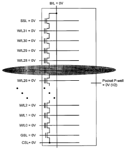
Page Erase Scheme 3
Table 8 and Figure 46 and 47 show bias conditions during page erase according
to a
page erase scheme 3. With the page erase scheme 3, unselected wordlines are
boosted to
nearly erase voltage Vers (a% of Vers when the substrate of the cell array
goes to Vers, a=
coupling ratio between the substrate and wordlines) for preventing the
unselected page(s)
from being erased while the selected wordline(s) is(are) biased to another
voltage for erasing
the selected page(s), for example, OV.
As shown in Figure 46 and 47, within the selected block
= Selected wordline(s) in the selected block is(are) biased to OV for erase.
-34-
CA 02644493 2008-09-25
WO 2007/109883 PCT/CA2007/000478
= Unselected wordline(s) in the selected block is(are) precharged and boosted
to a%
of Vers for erase inhibit (boosted voltage level on floated wordlines is
determined
by coupling ratio a between the substrate and wordlines, (x - 90%).
To prevent erasure of memory cells in unselected blocks, all wordlines in
unselected
blocks are floated during erase operations which is the same as the prior art
of patent
5,473,563. Therefore floated wordlines in unselected blocks are boosted to
nearly erase
voltage Vers by capacitive coupling between the substrate and wordlines in
unselected blocks
as erase voltage Vers is applied to the substrate. (The wordlines are boosted
to a% of Vers
when the substrate of the cell array goes to Vers; however, boosted voltage
level on floated
wordlines is determined by coupling ratio between the substrate and
wordlines.) The boosted
voltage on wordlines in unselected blocks reduces electric field between the
substrate and
wordlines; as a result, erasure of memory cells in unselected blocks is
prevented.
= All wordlines in unselected blocks are floating.
Table 8. Bias Conditions during Page/Multipage Erase - Page Erase Scheme 3
SELECTED BLOCK UNSELECTED BLOCK
BITLINES (B/L) CLAMPED TO Vers - 0.6V CLAMPED TO Vers - 0.6V
STRING SELECT LINE BOOSTED TO APPROX. BOOSTED TO APPROX.
(SSL) 90% Vers 90% Vers
SELECTED OV BOOSTED TO APPROX.
WORDLINE(S) 90% Vers
UNSELECTED BOOSTED TO APPROX. BOOSTED TO APPROX.
WORDLINE 90% Vers 90% Vers
GROUND SELECT BOOSTED TO APPROX. BOOSTED TO APPROX.
LINE (GSL) 90% Vers 90% Vers
COMMON SOURCE CLAMPED TO Vers - 0.6V CLAMPED TO Vers - 0.6V
LINE (CSL)
SUBSTRATE Vers Vers
(POCKET P-WELL)
-35-
CA 02644493 2008-09-25
WO 2007/109883 PCT/CA2007/000478
Figure 48 and 49 depict page erase conditions for unselected blocks, and
selected
page and unselected pages in the selected block.
= The string select line SSL, wordlines WLO to WL31 and the ground select line
GSL are driven by common signals of SS, SO to S31 and GS through pass
transistors TSS, TSO to TS31 and TGS which are commonly controlled by the
output signal BD_out of the block pre-decoder.
= Common signals of SS, SO to S31 and GS are connected to the drain of pass
transistors TSS, TSO to TS31 and TGS of entire blocks.
= The common source line CSL is connected across entire blocks.
= The selected common signal S (S27 in this example) corresponding to the
selected
page is biased to OV while unselected common signals S (SO - S26 & S28 - S31),
SS and GS are biased to V1. The common source line CSL is floated.
= The unselected output signal BD_out n-1 of unselected block pre-decoders
connected to the gate of all pass transistors TSS, TSO to TS31 and TGS are OV.
Therefore the string select line SSL, wordlines WLO to WL31 and the ground
select line GSL in unselected blocks are initially floated and boosted to
nearly 90%
(a) of the erase voltage Vers to nearly 90% ((x) by capacitive coupling
between the
cell substrate and wordlines when the cell substrate (pocket p-well) rises to
Vers.
This boosted voltage on all wordlines in unselected block prevent cell erase.
= The output signal BD_out of the selected block pre-decoder connected to the
gate
of all pass transistors TSS, TSO to TS31 and TGS is V2. Therefore the selected
wordline (W/L27 in this example) is biased to OV, driven by common signal S27
through the pass transistor TS27, which erases cells on the selected page.
= Unselected wordlines (W/LO - W/L26 & W/L28 - W/L31) in the selected block
are initially biased to V2-Vtn (Vtn: threshold voltage of pass transistors TSO
to
TS3 1) by common signals SO - S26 & S28 - S31 through pass transistors TSO -
TS26 & TS28 - TS31 (i.e. pass transistors drain= V 1, gate = V2, source=V2-
Vtn,
and V 1 _ V2). After that, unselected wordlines are boosted by capacitive
coupling
between the cell substrate and wordlines when the cell substrate (pocket p-
well)
rises to Vers. When unselected wordlines (i.e. source of pass transistors) are
boosted, pass transistors (TSO - TS26 & TS28 - TS3 1) are completely shut off
due to bias condition on pass transistors: drain= V 1, gate = V2, and source
=(a)
-36-
CA 02644493 2008-09-25
WO 2007/109883 PCT/CA2007/000478
of Vers (boosted voltage). Therefore the boosted high voltage on unselected
wordlines in unselected block is maintained during erase and prevents cell
erasure.
= V 1 must be equal to or greater than V2 to prevent leakage of the boosted
voltage
through the pass transistor, and allow the wordline to float.
In selecting V 1 and V2, it should be realized that the capacitive coupling
factor a is
dependent on individual wordline selection. Whereas, in an unselected block, a
is
approximately 90% at each wordline, a can be reduced adjacent to a selected
wordline. The
coupling is dependent on circuit characteristics but may reduce a to 50% as
illustrated in Fig.
50. Given the reduced coupling, the initial voltage of the wordline should be
higher in order
to assure that the wordline floats to a level that prevents erase.
To allow for floating, V 1 applied to the drain in the pass transistor must be
greater
than V2 applied to the gate. Thus:
V1>V2,
Vers > V2 > Vcc
Vboosted = (V2-Vtn) + a*(Vers - (V2-Vtn)).
If V2 were to only equal Vcc, the following boosted voltages of wordline WL28
(adjacent to
a selected page) and wordline WL27 (removed from the selected page) might
result:
If Vtn = 0.8V, Vcc = 2.5V, Vers = 20V and V2 = Vcc = 2.5V
WL28 (boosted voltage) = (V2-Vtn) + a (Vers - (V2-Vtn)) _
(2.5V-0.8V) + 0.5 * (20V - 1.7V) = 10.85V
WL27 (boosted voltage) = (V2-Vtn) + a (Vers - (V2-Vtn)) _
(2.5V-0.8V) + 0.9 * (20V - 1.7V) = 18.17V
It can be seen that WL27 is boosted to close to Vers and will thus avoid
accidental
erasure. However, wordline WL28 is only raised to < 11 volts, resulting in > 9
volts
difference between the wordline and the substrate voltage Vers. As a result,
unintended
erasure of WL28 is likely. To safely avoid erase, the wordline should be at
least about 70%
Vers, or 14 volts in this example.
By raising the gate voltage V2, and thus the drain voltage V 1, the initial
voltage on
the wordline is higher and thus the boosted voltage is higher, despite the
reduction in a. With
a higher voltage V2 of 10 volts, the following results in this example:
If Vtn = 0.8V, Vcc = 2.5V, Vers = 20V and V2 = lOV
WL28 (boosted voltage) = (V2-Vtn) + a (Vers - (V2-Vtn)) _
-37-
CA 02644493 2008-09-25
WO 2007/109883 PCT/CA2007/000478
(10V-0.8V) + 0.5 * (20V - 9.2V) = 14.6V
WL27 (boosted voltage) = (V2-Vtn) + a (Vers - (V2-Vtn)) _
(lOV-0.8V) + 0.9 * (20V - 9.2V) = 18.92V
In this case, the boosted voltage on the adjacent wordline WL28 is
sufficiently high at
14.6v. The reduced value of a and the acceptable voltage difference between
the wordline
and substrate will vary, thus varying the acceptable level of V2. However, in
general, V2
should be at least about 50% Vers. More generally, V2 and thus V 1 should be
closer to the
substrate voltage than to the select voltage applied to pass transistors of
selected wordlines.
Figure 49 shows multiple pages (wordline 1, 27, 29) in the selected block are
erased
at the same time using bias conditions of the page erase scheme 3.
Previously described Figure 34 illustrates a circuit schematic of block
decoder which
is one of possible examples for the page erase scheme 3 with V 1> V2.
The BDLCH_out is reset to OV when the RST_BD is high (actually short pulse)
and
latched when the LCHBD is high (actually short pulse) with valid row
predecoded address
signals of Xp, Xq, Xr and Xt.
The final output signal BD_out of the block pre-decoder is commonly connected
to
the gate of all pass transistors TSS, TSO to TS31 and TGS. The string select
line SSL,
wordlines WLO to WL31 and the ground select line GSL are driven by common
signals of
SS, SO to S31 and GS through pass transistors which are commonly controlled by
the output
signal BD_out of the block pre-decoder.
The local charge pump is a high voltage switching mean to provide V2 to the
output
signal BD_out of the block decoder. It consists of enhancement NMOS
transistor, depletion
NMOS transistor (DEP), native NMOS transistor (NAT) and a 2-input NAND gate.
The
output signal BD_out of the block decoder is raised to Vhv (=V2) when the
block decoder
latch output BDLCH_out is Vdd, HVenb is OV and the OSC is oscillated
Figure 51 shows the core timing of page erase or multiple page erase with the
page
erase scheme 3.
Basically the erase operation consists of three sub-periods as Erase Setup
(from tl to
t2), Erase (t2 to t3) and Erase Recovery (from t3 to t4) shown in Figure 51.
Erase Setup (tl to t2):
= The block decoder latch is reset by the RST BD pulse and the BDLCH out of
the
latch in the block decoder goes to OV.
-38-
CA 02644493 2008-09-25
WO 2007/109883 PCT/CA2007/000478
= The latch enable signal LCHBD of the block decoder is pulsed once row
predecoded signals Xp/Xq/Xr/Xt are valid.
= The BDLCH_out of the latch is set to Vdd when row predecoded signals
Xp/Xq/Xr/Xt are matched (i.e. selected).
= The output signal BD_out of the block pre-decoder is V2.
= The selected common signal S corresponding to the selected page is set to OV
while unselected common signals S, SS and GS are set to V I. The common source
line CSL is floated.
= The BD_out of unselected blocks are set to OV. As a result, all wordlines,
SSL,
GSL, CSL in unselected blocks are floated.
= The BD_out of the selected block is set to V2 and all pass transistors SST,
TSO to
TS3 1, GST are turned on. Therefore the selected wordline(s) is(are) biased to
OV
while unselected wordlines, SSL, GSL are precharged to V2-Vtn (Vtn: threshold
voltage of pass transistors).
Erase (t2 to t3):
= During this period, the cell substrate (pocket p-well) rises to erase
voltage Vers.
= The selected wordline for single page erase is or selected wordlines for
multiple
page erase in the selected block are biased to OV.
= The string select line SSL, ground select line GSL and unselected wordlines
in the
selected block are initially precharged to V2-Vtn, and then boosted to a% of
Vers
by capacitive coupling between the substrate and wordlines & SSL/GSL when the
cell substrate goes to Vers (the boosted voltage level on floated wordlines is
determined by coupling ratio (a) between the substrate and wordlines).
= The CLS and all bitlines (BLs) go to Vers due to junction forward bias from
the
substrate (PP-well) to the source (n+).
= During this period, all cells on the selected page (pages) is(are) erased.
Erasure of
memory cells in unselected wordlines in the selected block is prevented by the
boosted wordline voltage.
= All wordlines, SSL, GSL, CSL in unselected blocks are boosted to a% of Vers
by
capacitive coupling between the substrate and wordlines & SSL/GSL when the
cell substrate goes to Vers.
-39-
CA 02644493 2008-09-25
WO 2007/109883 PCT/CA2007/000478
= When unselected wordlines (i.e. drain of pass transistors) are boosted (i.e.
source
of pass transistor > V2-Vtn), pass transistors (TSO - TS26 & TS28 - TS3 1) are
completely shut off due to bias condition on pass transistors: drain =V 1>V2,
gate =
V2, and source = a Vers (boosted voltage). Therefore the boosted high voltage
on
unselected wordlines in unselected block is maintained during erase and
prevents
cell erasure.
Erase Recovery (t3 to t4):
= During this period, all high voltages on the cell substrate, unselected
selected
wordline, SSL, GSL, and CSL are discharged to the initial state (OV).
While this invention has been particularly shown and described with references
to
example embodiments thereof, it will be understood by those skilled in the art
that various
changes in form and details may be made therein without departing from the
scope of the
invention encompassed by the appended claims.
-40-