Note: Descriptions are shown in the official language in which they were submitted.
CA 02645781 2009-08-04
DUAL FUNCTION DATA REGISTER
FIELD OF THE INVENTION
[001] The invention is directed to non-volatile memories. More specifically,
the
invention is directed to data registers of non-volatile memories.
BACKGROUND OF THE INVENTION
[002] Over the past 30 years, anti-fuse technology has attracted significant
attention
of many inventors, IC designers and manufacturers. An anti-fuse is a structure
alterable to a
conductive state, or in other words, an electronic device that changes state
from not
conducting to conducting. Equivalently, the binary states can be either one of
high resistance
and low resistance in response to electric stress, such as a programming
voltage or current.
There have been many attempts to develop and apply anti-fuses in
microelectronic industry,
but the most successful anti-fuse applications to date can be seen in FGPA
devices
manufactured by Actel and Quicklogic, and redundancy or option programming
used in
DRAM devices by Micron. Anti-fuse technology is well known in the art, and
example anti-
fuse transistors are shown in Figures 1 to 5b.
[003] Anti-fuse memory is one type of one-time programmable (OTP) memory in
which the device can be permanently programmed (electrically) with data once.
This data is
programmed by an end user for a particular application. There are several
types of OTP
memory cells which can be used. OTP memories provide users with a level
flexibility since
any data can be programmed.
[004] Anti-fuse memory can be utilized in all one time programmable
applications,
including RF-ID tags. RF-ID tagging applications are gaining more acceptance
in the
industry, particularly in sales, security, transport, logistics, and military
applications for
-1-
CA 02645781 2009-08-04
example. The simplicity and full CMOS compatibility anti-fuse memory allows
for application
of the RF-ID tag concept to integrated circuit manufacturing and testing
processes.
Therefore, IC manufacturing productivity can be increased by utilizing anti-
fuse memory in
combination with an RF communication interface on every wafer and/or every die
on the
wafer allowing for contact-less programming and reading chip specific or wafer
specific
information during IC manufacturing and packaging, as well as during printed
circuit board
assembly.
[005] Figure 1 is a circuit diagram illustrating the basic concept of an anti-
fuse
memory cell, while Figures 2 and 3 show the planar and cross-sectional views
respectively,
of the anti-fuse memory cell shown in Figure 1. The memory cell of Figure 1
includes a pass,
or access transistor 10 for coupling a bitline BL to a bottom plate of anti-
fuse device 12. A
wordline WL is coupled to the gate of access transistor 10 to turn it on, and
a cell plate
voltage Vcp is coupled to the top plate of anti-fuse device 12 for programming
anti-fuse
device 12.
[006] It can be seen from Figures 2 and 3 that the layout of access transistor
10 and
anti-fuse device 12 is very straight-forward and simple. The gate 14 of access
transistor 10
and the top plate 16 of anti-fuse device 12 are constructed with the same
layer of polysilicon,
which extend across active area 18. In the active area 18 underneath each
polysilicon layer,
is formed a thin gate oxide 20, also known as a gate dielectric, for
electrically isolating the
polysilicon from the active area underneath. On either side of gate 14 are
diffusion regions
22 and 24, where diffusion region 24 is coupled to a bitline. Although not
shown, those of skill
in the art will understand that standard CMOS processing, such as sidewall
spacer formation,
lightly doped diffusions (LDD) and diffusion and gate silicidation, can be
applied. While the
classical single transistor and capacitor cell configuration is widely used, a
transistor-only
anti-fuse cell is further desirable due to the semiconductor array area
savings that can be
obtained for high-density applications. Such transistor-only anti-fuses must
be reliable while
simple to manufacture with a low cost CMOS process.
[007] Figure 4a shows a cross-sectional view of an anti-fuse transistor that
can be
manufactured with any standard CMOS process. Variants of this anti-fuse
transistor are
disclosed in commonly owned U.S. Patent Publication No. 2007/0257331. In the
presently
shown example, the anti-fuse transistor is almost identical to a simple thick
gate oxide, or
input/output MOS
-2-
CA 02645781 2008-12-23
WO 2008/077238 PCT/CA2007/002285
transistor with one floating diffusion terminal. The disclosed anti-fuse
transistor, also termed
a split-channel capacitor or a half-transistor, can be reliably programmed
such that the fuse
link between the polysilicon gate and the substrate can be predictably
localized to a
particular region of the device. The cross-section view of Figure 4a is taken
along the
channel length of the device, which in the presently described example is a p-
channel
device.
[009] Anti-fuse transistor 26 includes a variable thickness gate oxide 28
formed on
the substrate channel region 30, a polysilicon gate 32, sidewall spacers 34, a
field oxide
region 36, a diffusion region 38 and an LDD region 40 in the diffusion region
38. A bitline
contact 42 is shown to be in electrical contact with diffusion region 38. The
variable thickness
gate oxide 28 consists of a thick oxide and a thin gate oxide such that a
portion of the
channel length is covered by the thick gate oxide and the remaining portion of
the channel
length is covered by the thin gate oxide. Generally, the thin gate oxide is a
region where
oxide breakdown can occur. The thick gate oxide edge meeting diffusion region
38 on the
other hand, defines an access edge where gate oxide breakdown is prevented and
current
between the gate 32 and diffusion region 38 is to flow for a programmed anti-
fuse transistor.
While the distance that the thick oxide portion extends into the channel
region depends on
the mask grade, the thick oxide portion is preferably formed to be at least as
long as the
minimum length of a high voltage transistor formed on the same chip.
[0010] In this example, the diffusion region 38 is connected to a bitline
through a
bitline contact 42, or other line for sensing a current from the polysilicon
gate 32, and can be
doped to accommodate programming voltages or currents. This diffusion region
38 is formed
proximate to the thick oxide portion of the variable thickness gate oxide 28.
To further protect
the edge of anti-fuse transistor 26 from high voltage damage, or current
leakage, a resistor
protection oxide (RPO), also known as a salicide protect oxide, can be
introduced during the
fabrication process to further space metal particles from the edge of sidewall
spacer 34. This
RPO is preferably used during the salicidiation process for preventing only a
portion of
diffusion region 38 and a portion of polysilicon gate 32 from being salicided.
It is well known
that salicided transistors are known to have higher leakage and therefore
lower breakdown
voltage. Thus having a non-salicided diffusion region 38 will reduce leakage.
Diffusion region
38 can be doped for low voltage transistors or high voltage transistors or a
combination of
the two resulting in same or different diffusion profiles.
-3-
CA 02645781 2009-08-04
[0010] A simplified plan view of the anti-fuse transistor 26 is shown in
Figure 4b.
Bitline contact 42 can be used as a visual reference point to orient the plan
view with the
corresponding cross-sectional view of Figure 4a. The active area 44 is the
region of the
device where the channel region 30 and diffusion region 38 are formed, which
is defined by
an OD mask during the fabrication process. The dashed outline 46 defines the
areas in
which the thick gate oxide is to be formed via an OD2 mask during the
fabrication process.
More specifically, the area enclosed by the dashed outline 46 designates the
regions where
thick oxide is to be formed. OD simply refers to an oxide definition mask that
is used during
the CMOS process for defining the regions on the substrate where the oxide is
to be formed,
and OD2 refers to a second oxide definition mask different than the first.
Details of the
CMOS process steps for fabricating anti-fuse transistor 26 will be discussed
later. According
to an embodiment of the present invention, the thin gate oxide area bounded by
edges of the
active area 44 and the rightmost edge of the OD2 mask, is minimized. In the
presently shown
embodiment, this area can be minimized by shifting the rightmost OD2 mask edge
towards
the parallel edge of active area 44. Previously mentioned U.S. Patent
Publication No.
2007/0257331 describes alternate single transistor anti-fuse memory cells
which can be
used in a non-volatile memory array. Two transistor anti-fuse memory cells are
known in the
art, as shown in the example of Figures 5a and 5b.
[0011] Figure 5b shows a planar view of a two-transistor anti-fuse memory cell
48
having a minimized thin gate oxide area that can be manufactured with any
standard CMOS
process, according to an embodiment of the present invention. Figure 5a shows
a cross-
sectional view of the memory cell 48 of Figure 5b, taken along line B-B. Two-
transistor anti-
fuse memory cell 48 consists of an access transistor in series with an anti-
fuse transistor.
The access transistor includes a polysilicon gate 50 overlying a thick gate
oxide 52, which
itself is formed over the channel 54. On the left side of the channel 54 is a
diffusion region 56
electrically connected to a bitline contact 58. On the right side of the
channel 54 is a common
diffusion region 60 shared with the anti-fuse transistor. The anti-fuse
transistor includes a
polysilicon gate 62 overlying a thin gate oxide 64, which itself is formed
over the channel 66.
Dashed outline 68 represents the OD2 mask which defines the area where thick
oxide is to
be formed. The thick gate oxide 52 can correspond to that used for high
voltage transistors
while the thin gate oxide 64 can correspond to that used for low voltage
transistors. It is well
known that polysilicon gates 50 and 62 can be independently controlled, or
alternatively can
be connected to each other as shown in Figure 5b. In the example of Figure 5b,
both
-4-
CA 02645781 2009-08-04
polysilicon gates 50 and 62 are part of the same polysilicon structure, and
connected to a
wordline through wordline contact 70. Both diffusion regions 56 and 60 can
have LDD
regions, which can be identically doped or differently doped, depending on the
desired
operating voltages to be used. Commonly owned U.S. Patent Publication No.
2007/0257331
filed on June 13, 2007 describes alternate two-transistor anti-fuse memory
cells which can
be used in a non-volatile memory array.
[0012] The programming speed of OTP memories is relatively slow, since each
programming cycle will attempt to program a certain number of data words at
the same time.
Following each programming cycle is a program verify cycle to ensure that the
data words
were successfully programmed. Any bits that do not pass the program verify
step are
reprogrammed. This process continues until all the memory cell states have
been
successfully programmed. Figure 6a shows how an unprogrammed anti-fuse memory
cell,
such as anti-fuse transistor 26, is programmed. Anti-fuse transistor 26 has
its gate terminal
connected to a wordline WL and its single diffusion region connected to a
bitline BL.
Programming is effected by biasing the bitline to VSS and driving the wordline
to a high
voltage level VPP. VPP is selected based on the process technology and
thickness of the
thin gate oxide that is sufficient for forming a conductive link between the
polysilicon gate and
the channel region.
[0013] A successfully programmed anti-fuse transistor 26 is shown in Figure
6b,
where a conductive link 72 is formed between the polysilicon gate and the
channel region.
Conductive link 72 is schematically represented as a resistive connection
between the
wordline and the channel region under the thin gate oxide region of anti-fuse
transistor 26.
Therefore a programmed anti-fuse transistor having a conductive link stores
one logic state
of one bit of data. Accordingly, an unprogrammed anti-fuse transistor will by
default store the
other logic state of one bit of data. To prevent programming of the anti-fuse
transistor 26, the
bitline is biased to VDD while the wordline is driven to VPP. This will be
sufficient for
inhibiting the conductive link from forming.
[0014] Reading the anti-fuse transistor is achieved by driving the wordline to
a read
voltage VREAD, and by precharging the bitline to VSS, as shown in Figure 7. If
the anti-fuse
transistor 26 has a conductive link 72, then the wordline will pull the
bitline towards the
VREAD voltage level via the conductive link 72 and the positive gate voltage
of the anti-fuse
transistor. This bitline voltage can be sensed and amplified by sense
amplifier circuits. On
-5-
CA 02645781 2008-12-23
WO 2008/077238 PCT/CA2007/002285
the other hand, if the anti-fuse transistor 26 is not programmed, ie. does not
have a
conductive link 72, then the bitline will remain at approximately VSS.
[0016] Most electrically programmable non-volatile memories, such as Flash,
EEPROM or anti-fuse memories, require the use of high voltages to program the
memory
cells. These high voltages are generated on chip and distributed to wordlines
and/or bitlines
during programming operations. Depending on the architecture of the memory,
any number
of words can be programmed simultaneously, where each word is made up of a
predetermined number of bits. Assuming that the memory cells start in the
unprogrammed
state, logic 0 for example, only memory cells for storing a logic 1 state
actually undergo
programming. The number of logic 1 states to be programmed at the same time
depends on
the data to be programmed. Because a large number of bits may be programmed
simultaneously, the finite on-chip high voltage generators may not have
sufficient current to
program all the selected memory cells. Hence, after a first program cycle, the
cells subjected
to programming must be verified to ensure that they were successfully
programmed.
[0017] Verification is done by reading out the memory cells and comparing
their
stored logic states (logic 0 or 1) to the desired programmed state (logic 1
for example). If
specific bits were not successfully programmed, as determined by the program
verify cycle,
then the programming cycle is repeated. However, there is no need to re-
program cells
which were successfully programmed. This is especially problematic for anti-
fuse transistors.
A programmed anti-fuse transistor has a conduction path formed between its
wordline and its
bitline, thus repeating a program cycle on such a cell will draw more current
away from the
cells where programming is still required. Hence, those memory cells must be
excluded from
the next programming cycle. This iterative program-verify-program sequence
continues until
every memory cell to be programmed has been deemed to be successfully
programmed.
[0018] Figure 8 is a block diagram of a simplified anti-fuse memory device of
the prior
art, illustrating the logic circuits required for implementing program verify
operations. The
anti-fuse memory device of Figure 8 includes a memory array 80 consisting of
anti-fuse
memory cells, or other non-volatile memory cells, connected to wordlines and
bitlines.
Wordline drivers 82 apply the read and programming voltage levels to the
wordlines, while
column decoders and sense amplifiers 84 are coupled to the bitlines for
sensing and
multiplexing the sensed data to a data register 86. The data register 86 is
primarily
responsible for storing data to be programmed and for storing read data. The
program-verify
-6-
CA 02645781 2008-12-23
WO 2008/077238 PCT/CA2007/002285
circuits include additional latch circuits, which can be a second data
register 88, and
comparison logic 90. In use program data P_DATA is received by data register
86, which is
also stored in the second data register 88. Those skilled in the art will
understand that other
circuits required for proper operation of the memory device are intentionally
omitted, in order
to simplify the schematic.
[0019] Once a programming cycle has been completed, the data is read out from
the
memory cells being programmed, and stored in data register 86. The comparison
logic 90
then compares each bit position of data registers 86 and 88 to each other. If
all the bit
positions match, meaning that each bit position was successfully programmed,
then the
status signal STATUS will have a logic level indicating that all bits were
programmed.
Otherwise, if just one bit position did not successfully program, then the
status signal
STATUS will have another logic level, indicating that at least one bit was not
properly
programmed. Then further program cycles are executed, while the successfully
programmed
bits are masked, or inhibited from further programming.
[0020] One of the main problems with this program verify scheme is that the
circuit
implementation consumes too much valuable circuit area. Mainly, a second data
register is
required for storing the program data, which will be very large if the word to
be programmed
is very wide. The logic required to disable successfully programmed bit
positions can be
complex, as can be the comparison logic used to detect the failed programming
of at least
one bit position. Those skilled in the art will understand that increased
circuit area will directly
impact the manufacturing cost of the device as more chip area is required per
device.
[0021] It is, therefore, desirable to provide a program verify scheme that
does not
require a second data register, and can simplify program verification
operations.
SUMMARY OF THE INVENTION
[0022] It is an object of the present invention to obviate or mitigate at
least one
disadvantage of prior OTP memories. More specifically, it is an object of the
present
invention provide a data register that can integrate program verify operations
with data
storage functionality.
[0023] In a first aspect, the present invention provides a data register
stage. The data
register stage includes a data storage circuit and a status circuit. The data
storage circuit
-7-
CA 02645781 2008-12-23
WO 2008/077238 PCT/CA2007/002285
having a first latch and a second latch arranged in a master-slave flip-flop
configuration for
shifting in data serially from a serial input terminal and for shifting out
data from a serial
output terminal. The shifting operations are controlled by phase adjustable
clock signals. The
status circuit detects opposite logic states stored in the first latch and the
second latch, and
combines an output corresponding to the detected opposite logic states with a
previous local
status signal to provide a local status signal. The previous local status
signal corresponds to
detected opposite logic states stored in a previous data register stage. In an
embodiment of
the present aspect, the data storage circuit further includes a parallel data
input circuit for
coupling parallel data to an input of the first latch in response to a write
signal, and a parallel
data output terminal coupled to an output of the second latch. Further
included is a program
inhibit circuit for reversing the logic state stored in the first latch if the
second latch stores a
specific logic state. The program inhibit circuit includes a first transistor
and a second
transistor serially connected between a voltage supply and an input of the
first latch. The first
transistor gate receives an enable signal and the second transistor gate is
coupled to an
output of the second latch.
[0024] In another embodiment, the status circuit includes an XOR gate for
comparing
the logic state of the second latch to an inverted logic state of the first
latch, and an AND
gate for combining the XOR gate output with the previous local status signal
to provide the
local status signal. The status circuit will further detect matching logic
states stored in the first
latch and another first latch of the previous data register stage for
providing a second local
status signal. The status circuit includes an AND gate for combining the logic
state of the first
latch with a second previous local status signal corresponding to the logic
state of a second
first latch of the previous data register stage, for providing the second
local status signal. In
yet a further embodiment, the first latch output is coupled to a sense
amplifier input and the
second latch input is coupled to a sense amplifier output. The phase
adjustable clock signals
can include first and second clock signals generated by a clock controller in
response to a
source clock and an active logic level of a shift enable signal. The clock
controller can
include a first AND gate and a second AND gate. The first AND gate generates
the first clock
signal in response to the source clock and the active logic level of the shift
enable signal. The
second AND gate generates the second clock signal in response to an inverted
source clock
and the active logic level of the shift enable signal.
-8-
CA 02645781 2008-12-23
WO 2008/077238 PCT/CA2007/002285
[0025] In a second aspect, the present invention provides a non-volatile
memory
device. The non-volatile memory device includes a memory array having non-
volatile
memory cells connected to wordlines and bitlines, bitline sense amplifiers,
and a data
register. The bitline sense amplifiers are coupled to the columns for biasing
the bitlines in
response to program data in a program operation, and sense a read voltage of
the bitlines in
a read operation to provide read data. The data register concurrently stores
the program
data and the read data, and compares the stored program data to the stored
read data. The
data register further provides a status signal corresponding to a successful
program
operation when the stored program data and the stored read data are opposite
logic levels.
In an embodiment of the present aspect, the data register includes a first
register stage and a
second register stage serially connected to each other for serially shifting
one of the program
data and the read data through a serial output port coupled to the second
register stage. The
first register stage and the second register stage can each include a data
storage circuit and
a status circuit. The data storage circuit has a first latch and a second
latch arranged in a
master-slave flip-flop configuration for shifting in data serially from a
serial input terminal and
for shifting out data from a serial output terminal. The shifting operations
are controlled by
phase adjustable clock signals. The status circuit detects opposite logic
states stored in the
first latch and the second latch, and combines an output corresponding to the
detected
opposite logic states with a previous local status signal to provide a local
status signal. The
previous local status signal corresponds to detected opposite logic states
stored in a
previous data register stage.
[0026] In yet a further embodiment, a clock controller is provided for
generating the
phase adjustable clock signals in response to a source clock and a shift
enable signal. The
program data is shifted out through the serial output port when the shift
enable signal is
activated while the source clock is at a first logic level, and the read data
is shifted out
through the serial output port when the shift enable signal is activated while
the source clock
is at a second logic level. The data storage circuit further includes a
parallel data input circuit
for coupling parallel data to an input of the first latch in response to a
write signal, and a
parallel data output terminal coupled to an output of the second latch.
[0027] According to another embodiment, the status circuit includes a data
match
circuit for detecting opposite logic states stored in the first latch and the
second latch. The
data match circuit includes an XOR gate and an AND gate. The XOR gate compares
the
-9-
CA 02645781 2008-12-23
WO 2008/077238 PCT/CA2007/002285
logic state of the second latch to an inverted logic state of the first latch.
The AND gate
combines the XOR gate output with the previous local status signal to provide
the local
status signal. A program inhibit circuit is provided for changing the logic
state stored in the
first latch to a program inhibit logic state if the second latch stores read
data corresponding to
a successfully programmed memory cell. The status circuit includes a reprogram
verify circuit
for providing a second local status signal when the first latch and a previous
second local
status signal have logic states corresponding to the program inhibit logic
state. The previous
second local status signal is provided by the previous data register stage. In
one aspect of
the present embodiment, the data register includes program verify logic for
providing the
status signal corresponding to a successful program operation when the local
status signal is
at a logic level corresponding to the detected opposite logic states. In a
second aspect of the
present embodiment, the data register includes program verify logic for
providing the status
signal corresponding to a successful program operation when the second local
status signal
is at a logic level corresponding to the program inhibit logic state.
[0028] In yet a further aspect of the present embodiment, the data register
can
include program verify logic for providing the status signal corresponding to
a successful
program operation when the local status signal is at a logic level
corresponding to the
detected opposite logic states and the second local status signal is at a
logic level
corresponding to the program inhibit logic state. The program inhibit circuit
can include a first
transistor and a second transistor serially connected between a voltage supply
and an input
of the first latch, the first transistor gate receiving an enable signal and
the second transistor
gate being coupled to an output of the second latch. The reprogram verify
circuit includes an
AND gate for combining the logic state of the first latch with the previous
second local status
signal to provide the second local status signal.
[0029] Other aspects and features of the present invention will become
apparent to
those ordinarily skilled in the art upon review of the following description
of specific
embodiments of the invention in conjunction with the accompanying figures.
BRIEF DESCRIPTION OF THE DRAWINGS
[0030] Embodiments of the present invention will now be described, by way of
example only, with reference to the attached Figures, wherein:
Fig. 1 is a circuit diagram of an anti-fuse memory cell;
-10-
CA 02645781 2008-12-23
WO 2008/077238 PCT/CA2007/002285
Fig. 2 is a planar layout of the anti-fuse memory cell of Figure 1;
Fig. 3 is a cross-sectional view of the anti-fuse memory cell of Figure 2
along
line x-x;
Fig. 4a is a cross-sectional view of a variable thickness gate oxide anti-fuse
transistor;
Fig. 4b is a planar layout of the variable thickness gate oxide anti-fuse
transistor of Figure 4a;
Fig. 5a is a cross-sectional view of a two-transistor anti-fuse memory cell;
Fig. 5b is a planar layout of the two-transistor anti-fuse memory cell of
Figure
5a;
Fig. 6a is a schematic of the anti-fuse transistor of Figure 4a under
programming conditions;
Fig. 6b is a schematic of a programmed anti-fuse transistor of Figure 4a;
Fig. 7 is a schematic of a programmed anti-fuse transistor of Figure 4a under
read conditions;
Fig. 8 is a block diagram of a prior art non-volatile memory device having
program verify circuitry;
Fig. 9 is a block diagram of a non-volatile memory device having a dual
function data register with integrated program verify circuitry, according to
an
embodiment of the present invention;
Fig. 10 is a block diagram showing details of the dual function data register
of
Figure 9;
Fig. 11 is a circuit schematic of a folded bitline sensing scheme for an anti-
fuse memory array;
Fig. 12 is a circuit schematic of one register stage of the dual function data
register shown in Figure 10, according to an embodiment of the present
invention;
Fig. 13 is a circuit schematic of the clock controller shown in Figure 9,
according to an embodiment of the present invention;
Fig. 14 is a circuit schematic of the program verify logic shown in Figure 10,
according to an embodiment of the present invention;
Fig. 15 is a flow chart of a method for executing a program verify operation
using the dual function data register, according to an embodiment of the
present
invention;
-11-
CA 02645781 2008-12-23
WO 2008/077238 PCT/CA2007/002285
Fig. 16 is an illustration of an example serial shift operation of the dual
function data register of Figure 12 with a corresponding sequence diagram of
the
clock signals;
Fig. 17 is an illustration of another example serial shift operation of the
dual
function data register of Figure 12 with a corresponding sequence diagram of
the
clock signals;
Fig. 18 is a block diagram of a power up detection system, according to an
embodiment of the present invention;
Fig. 19 is an illustration of the data states stored in memory cells of the
test
memory array of Figure 18;
Fig. 20a is a plan view of mask programmed skewed ROM cells, according to
an embodiment of the present invention;
Fig. 20b is a plan view of mask programmed two transistor skewed ROM cells,
according to an embodiment of the present invention;
Fig. 21 a is a plan view of the test memory array of Figure 18 using the mask
programmed skewed ROM cells of Figure 20a;
Fig. 21 b is a plan view of the test memory array of Figure 18 using the mask
programmed two transistor skewed ROM cells of Figure 20b;
Fig. 21c is an illustration of the data states stored in the skewed ROM cells
of
Figure 21 a;
Fig. 22 is a circuit schematic of a register stage of the dual function data
register of Figure 18, according to an embodiment of the present invention;
Fig. 23 is a flow chart of a power up detection method using the power up
detection system of Figure 18;
Fig. 24 is an illustration of a serial shift operation of the dual function
data
register of Figure 18 with a corresponding sequence diagram of the clock
signals;
and,
Fig. 25 is a circuit schematic of one register stage of the dual function data
register, according to an alternate embodiment of the present invention.
-12-
CA 02645781 2008-12-23
WO 2008/077238 PCT/CA2007/002285
DETAILED DESCRIPTION
[0031] Generally, the present invention is directed to a dual function serial
and
parallel data register with integrated program verify functionality. The dual
function serial and
parallel operation gives the user the option for serial or parallel data
interfacing in a single
circuit, while integrating program verify functionality for reducing circuit
logic overhead by
utilizing the master and slave latching circuits of the data register to
concurrently store two
different words of data. In a program verify operation, the master latch
stores program data
and the slave latch will receive and store read data. Comparison logic in each
register stage
will compare the data of both latches and integrate the comparison result to
that of the
previous register stage. The final single bit result will indicate the
presence of at least one bit
that has not been programmed. If reprogramming is necessary, automatic program
inhibit
logic in each stage will prevent successfully programmed bits from being re-
programmed in
each subsequent reprogram cycle. Because two data words can be concurrently
stored in
the dual function data register embodiments of the present invention, either
data word can be
serially clocked out by selectively starting the shift operations on either
the low or high active
logic level of a clock signal. Significant circuit area is conserved relative
to the prior art
program verify schemes because a second data register is not required.
[0032] Figure 9 is a block diagram of a non-volatile memory device having a
dual
function serial and parallel data register according to an embodiment of the
present
invention. The non-volatile memory device 100 includes a memory array 102
consisting of
non-volatile memory cells connected to wordlines and bitlines, such as the
anti-fuse memory
cells shown in Figures 4a, 4b, 5a and 5b. It is noted that memory array 102
can be
implemented with other non-volatile memory cells, such as EEPROM or Flash
memory cells.
Wordline drivers 104 drive the wordlines to read or programming voltages,
while column
decoder and sense amplifiers 106 are coupled to the bitlines for sensing and
multiplexing the
sensed data to the dual function serial and parallel data register 108. A
clock controller 110
provides the clock signals to control the shifting function of the dual
function serial and
parallel data register 108.
[0033] Dual function serial and parallel data register 108, referred simply as
the dual
function data register 108 from this point forward, is configured to
facilitate execution of many
useful features. Dual function data register 108 can receive and provide data
in both a
parallel format and a serial format. This is to accommodate systems that
memory device 100
- 13 -
CA 02645781 2008-12-23
WO 2008/077238 PCT/CA2007/002285
is integrated in or used with, the flexibility for a parallel or serial
interface with the same
design. For a parallel data interface, parallel data P_DATA can be
asynchronously coupled
to and from dual function data register 108 via a bidirectional bus.
Alternately, separate input
and output busses can be used for carrying the parallel input data and the
parallel output
data, respectively. For a serial data interface, serial input data is received
at input port
S_DATA_IN and serial output data is provided at output port S_DATA_OUT.
Shifting of serial
data is controlled by phase adjustable clock signals CK1 and CK2, which are
controlled by
source clock SCK and a shift enable signal SEN. As will be discussed later,
one of two data
words stored in dual function data register 108 can be synchronously shifted
out by
controlling the time that SEN is driven to the active logic level relative to
SCK. Logic for
automatically inhibiting programmed cells from being further programmed, and
cascaded
logic for generating the program verify status signal STATUS, is integrated
into dual function
data register 108 for program verify operations.
[0034] Figure 10 is a block diagram showing further details of dual function
data
register 108, according to an embodiment of the present invention. The dual
function data
register can be used for temporary data storage for two different data words,
to provide data
to be programmed in the anti-fuse memory cell array, and to store data
retrieved from the
memory cell array. It is also used for comparing the data to be programmed
with contents of
the programmed cells for program verify purposes. The dual function data
register 108 is an
n-bit serial/parallel shift register, where n is an integer value greater than
0, and consists of
individual register stages. Figure 10 shows first register stage 200, second
register stage 202
and the last (nth) register stage 204. Each register stage has a parallel
input P_IN controlled
by a WRITE signal, a parallel output P_OUT, and receives clock signals CK1 and
CK2. The
WRITE signal allows for asynchronous parallel write to the register, while CK1
and CK2 allow
shifting of the register contents in and out synchronously with a source clock
SCK (not
shown). Each register stage has a serial input terminal for receiving data
from a previous
register stage, and a serial output terminal for providing data to a
subsequent register stage.
For example, register stage 202 has a serial input terminal for receiving
serial output data
S1_OUT from register stage 200, and has a serial output terminal for providing
serial output
data S2_OUT to the next register state. The first register stage 200 receives
serial input data
through input port S_IN, and provides serial output data through output port
S_OUT.
-14-
CA 02645781 2008-12-23
WO 2008/077238 PCT/CA2007/002285
[0035] With specific reference to register stage 202, each register stage will
provide
program data to a memory cell through terminal SA1_in during a program
operation, while
receiving read data from a memory cell through terminal SA_out during a read
operation or a
program verify operation. Those skilled in the art will understand that the
program data can
be provided either directly to the selected bitline or to the selected bitline
through a sense
amplifier, and that the read data is provided from a sense amplifier. Each
register stage can
provide two program verify signals, noted as C1_a and C1_b for register stage
200 for
example. C1_a indicates if the initial programming operation was successful
for all bits, while
C1_b indicates if a re-programming operation is successful for all bits. The
reason for having
two different comparison results will be discussed in more detail later. The
two comparison
results from each register stage are fed to a subsequent register stage, which
then combines
the result with its own comparison results. The combined result is then fed to
the next stage.
A final stage of logic, the program verify logic 206, receives the last two
comparison results
from the last register stage 204, and generates a single STATUS signal. The
STATUS signal
will be used to indicate if an initial program operation was successful or if
a subsequent re-
program operation was successful. Program verify logic 206 can be implemented
outside of
dual function data register 108.
[0036] Figure 11 is a schematic of a portion of a folded bitline anti-fuse
memory array
102 and its associated bitline sensing circuitry 106 of Figure 9. In order to
simplify the
schematic, only one folded bitline pair BL/BL* and two wordlines are shown.
Column decoder
circuitry is not shown for selectively coupling multiple folded bitline pairs
to the bitline sense
amplifier circuitry. Folded bitline anti-fuse memory array 210 includes
wordlines WLO and
WL1 connected to the gate terminals of n-channel anti-fuse transistors 212 and
214, n-
channel isolation transistors 216 and 218 for coupling the upper portion of
the bitlines to the
lower portion of the bitlines in response to signal ISO, and bitline sensing
circuitry. The bitline
sensing circuitry includes a precharge circuit 220, a reference charge circuit
222, and a
bitline sense amplifier 224.
[0037] The precharge circuit 220 includes two n-channel precharge transistors
226
and 228 connected in series between BL and BL* and having their gate terminals
connected
to precharge signal BLPCH. The shared source/drain terminal of precharge
transistors 226
and 228 receives a precharge voltage VPCH. In operation, both precharge
transistors 226
-15-
CA 02645781 2008-12-23
WO 2008/077238 PCT/CA2007/002285
and 228 will turn on to precharge bitlines BL and BL* to VPCH in response to
an active high
logic level of BLPCH, in preparation for a read operation.
[0038] The reference charge circuit 222 includes n-channel steering
transistors 230
and 232 connected in series between BL and BL*, a capacitance circuit
implemented as an
n-channel transistor 234, and a p-channel precharge transistor 236. Steering
transistor 230
has its gate terminal connected to even selection signal E_REF, while steering
transistor
232 has its gate terminal connected to odd selection signal O_REF. Capacitance
circuit 234
has its gate terminal connected to voltage supply VCC, and is connected in
series with
precharge transistor 236 between the shared source/drain terminal of steering
transistors
230 and 232 and voltage supply VCC. Precharge transistor 236 has its gate
terminal
connected to a precharge or enable signal PCH*. Generally, capacitance circuit
234 will be
precharged when a low logic level PCH* pulse is received. The duration of the
PCH* pulse
can be predetermined based on the size of transistor 234 and the desired
reference charge
to be provided. Once precharged, either steering transistor 230 or 232 is
turned on to couple
the reference charge of capacitance circuit 234 to the corresponding bitline.
By example, the
charge being added to a bitline can be approximately 50 millivolts. It is
noted that signals
E_REF and O_REF can be controlled by the same even/odd addressing bit used for
selecting WLO or WL1. In one embodiment, activation of WLO will cause E_REF to
be
activated, thereby coupling the reference charge to the complementary bitline.
[0039] The bitline sense amplifier 224 consists of a standard cross-coupled
inverter
circuit that is well known in the art. The circuit includes p-channel
transistors both connected
in series to respective n-channel transistors. The common drain terminal of
the p-channel
transistors receives a high logic level enable signal H_EN, while the common
source terminal
of the n-channel transistors receives a low logic level enable signal L_EN.
H_EN can be a
lowered internal VCC level, while L_EN can be a VSS level. The operation of
bitline sense
amplifier 224 in the DRAM art is well known. When enable signals H_EN and L_EN
are
activated, either at the same time or at different times, bitline sense
amplifier 224 will sense a
small voltage differential between BL and BL*, and quickly drive both BL and
BL* to the full
logic level states of HEN and L_EN.
[0040] Because bitline sense amplifier 224 is connected to both bitlines BL
and BL*,
the logic state being programmed or read from the memory array will depend on
the memory
cell that is accessed. For example, if both anti-fuse transistors 212 and 214
store a logic 1,
-16-
CA 02645781 2008-12-23
WO 2008/077238 PCT/CA2007/002285
bitline sense amplifier 224 will latch two different logic states depending on
which anti-fuse
transistor is accessed. Therefore, a data state corrector 238 is used for
ensuring that the
voltage level corresponding to logic 1 and 0 states is read and programmed. In
the present
example, if WLO is activated to read anti-fuse transistor 214, then signal
EVEN will be at the
logic state for coupling BL* to gating transistor 242. Alternately, of WL1 is
activated to read
anti-fuse transistor 212, then signal EVEN will be at the opposite logic state
for coupling BL
to gating transistor 242. The operation of data state corrector 238 is similar
when program
data is to be coupled to either BL or BL* from gating transistor 240. Data
state corrector 238
can be implemented as a simple bi-directional multiplexor controlled by signal
EVEN, which
can be related to the address used to select wordline WLO and WL1. Signal EVEN
can be
related to signals E_REF and O_REF as well. Data to be programmed to the
bitlines is
provided through n-channel gating transistor 240 which is coupled to SAi_in
and controlled
by program signal PGM. Data to be read from the bitlines is provided through n-
channel
gating transistor 242 which is coupled to SAi_out and controlled by read
signal READ.
Accordingly, gating transistor 240 is turned on during a program operation
while gating
transistor 242 is turned on during a read operation. Variable "i" is an
integer value between 1
and max number n, which represents the specific register stage of the dual
function data
register 108. Terminals SAi_in and SAi_out are connected to one register stage
of the dual
function data register 108.
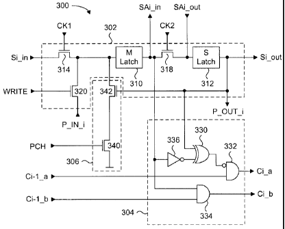
[0041] Figure 12 is a circuit schematic of one register stage of the dual
function data
register 108 shown in Figure 10, according to an embodiment of the present
invention. Data
register stage 300 includes two main sections. The first section is the data
storage circuit
302, which is responsible for data input, output and latching operations. The
second section
includes status circuit 304 and auto-program inhibit circuit 306. All the
register stages of the
dual function data register 108 shown in Figure 10 will have the same circuit
configuration
shown in Figure 12. The data storage circuit 302 will now be described. It is
noted that
variable "i" in the signal names denotes the register stage it is associated
with, where "i" is
any integer value greater than 0 and less than n, where n is the maximum
number of register
stages in the dual function data register 108.
[0042] Data storage circuit 302 includes a master latch 310 and a slave latch
312
connected as a master-slave flip-flop, serial input gating device 314,
transfer gating device
318, and a parallel input gating device 320. Latches 310 and 312 can be
implemented as
-17-
CA 02645781 2008-12-23
WO 2008/077238 PCT/CA2007/002285
simple cross-coupled inverter circuits with a non-inverting output relative to
its input, but
slave latch 312 will be configured to be overwritten by master latch 310 in a
program
operation. Those skilled in the art will understand that transistor sizing can
be configured to
achieve this desired effect. Gating devices 314 and 318 are shown as n-channel
transistors,
but can be transmission gates or p-channel devices. Gating device 314 has its
gate terminal
connected to clock signal CK1, while gating device 318 has its gate terminal
connected to
clock signal CK2. CK1 and CK2 are controlled clock signals. Gating devices 314
and 318 are
controlled by CK1 and CK2 to shift data serially from the serial input
terminal Si_in to the
master latch 310, or from master latch 310 to slave latch 312, or from slave
latch 312 to
serial output terminal Si-out. Parallel input data P_IN_i is provided to the
input of master
latch 310 via gating device 320 when signal WRITE is at the active logic
level, which in the
present example is the high logic level. Parallel output data P_OUT_i is
provided from the
output of slave latch 312. The output of master latch 310, typically being
program data, is
coupled to a sense amplifier via terminal SAi_in, while read data from the
sense amplifier is
provided from terminal SAi_out and stored by slave latch 312.
[0043] As previously mentioned, the program verify scheme utilizes two related
circuits; the status circuit 304 and the auto-program inhibit circuit 306. The
status circuit 304
includes an XOR logic gate 330, AND logic gates 332 and 334, and an inverter
336. Inverter
336, XOR gate 330 and AND gate 332 form a data match circuit, while AND gate
334 forms
a reprogram verify circuit. XOR gate 330 has a first input connected to the
output of slave
latch 312 and a second input coupled to an output of master latch 310 via
inverter 336. The
output of XOR gate 330 is connected to a first inverted input of AND gate 332,
which has its
second input connected to input Ci-1_a. The output of AND gate 332 is a local
status signal
Ci_a. Input Ci-1_a is the local status signal of the previous register stage,
and more
specifically, the output of an AND gate 332 of the previous register stage.
Local status signal
Ci_a is connected to the second input of an AND gate 332 of the next register
stage. AND
gate 334 has a first input connected to the output of master latch 310 and a
second input
connected to input Ci-1_b, which is another local status signal from the
previous register
stage. The output of AND gate 334 is second local status signal Ci_b. Input Ci-
1_b is
connected to the output of an AND gate 334 of the previous register stage,
while Ci_b is
connected to the second input of an AND gate 334 of the next register stage.
AND gate 334
simply combines the logic state of master latch 310 with the logic state of
the master latch
310 of the previous register stage.
-18-
CA 02645781 2008-12-23
WO 2008/077238 PCT/CA2007/002285
[0044] XOR gate 330 compares the logic state of slave latch 312 to the
inverted state
of master latch 310. The comparison result of XOR gate 330 is then compared
and combined
with the comparison result from the previous register stage using AND gate
332. This portion
of the circuit is used to verify if the initial programming operation was
successful or not speed
up memory testing and verification process. It compares all the bits in a row
simultaneously
and the result is combined into a single output signal STATUS in Figure 14. In
a compare
operation, STATUS goes high upon COMP activation and remains HIGH if all data
bits
match (logic 1 propagates through all data register stages) or goes LOW if a
mismatch is
detected (when any of the outputs of the XOR gates exit logic 1 instead of 0,
indicating
mismatch between the inverted data from master latch and data from slave
latch). STATUS
remains active for as long as COMP is held HIGH and is reset to its default
LOW state when
COMP is LOW. Before the COMP operation, master latches of the data register
should be
reloaded with the original desired data, and the slave latches should contain
the actual data
read from the memory cells after programming.
[0045] The auto-program inhibit circuit 306 is used to verify if a
reprogramming
operation was successful or not, when the auto-program inhibit circuit 306 is
engaged after
an initial program operation failure. The auto-program inhibit circuit 306
includes a precharge
device 340 and a coupling device 342 connected in series between a voltage
supply such as
VDD and the input of master latch 310. Both devices 340 and 342 are shown as
being n-
channel transistors in the present embodiment. The gate of precharge device
340 is
connected to precharge signal PCH and the gate of coupling device 342 is
connected to the
output of slave latch 312. The selection of the voltage supply depends on the
logic state
stored by master latch 310 for selecting a memory cell to be programmed. For
example, if
master latch 310 stores a logic 0 (VSS) to indicate programming of the memory
cell
connected to that bitline, then the voltage supply connected to precharge
device 340 will be
VDD. Hence, VDD is the logic state stored in a master latch 310 for a memory
cell that is not
to be programmed. The auto-program inhibit circuit will therefore change the
state of the
master latch 310 if the memory cell was successfully programmed. In the
present example, a
successfully programmed memory cell will result in slave latch 312 storing a
high a logic
state in a program verify read operation following a program operation.
Therefore, when PCH
is driven to the high logic level, VDD is coupled to the input of master latch
310 to flip its
state.
-19-
CA 02645781 2008-12-23
WO 2008/077238 PCT/CA2007/002285
[0046] The data shifting operation and the logic comparison operation of the
data
register stage 300 will be discussed later in further detail. Prior to such a
discussion, a
description of the clock controller 110 of Figure 9 follows. Figure 13 is a
circuit schematic of
the clock controller 110, according to an embodiment of the present invention.
Clock
controller 110 includes a first AND logic gate 350 and a second AND logic gate
352. Both
AND gates 350 and 352 have a first input for receiving shift enable signal
SEN, while AND
gate 352 has a second input for receiving source clock signal SCK and AND gate
350 has a
second input for receiving the complement of SCK. The output of AND gate 350
is clock
signal CK2 and the output of AND gate 352 is clock signal CK1. Therefore while
SEN is at
the inactive low logic state, the output of AND 350 and CK1 will be at the
inactive low logic
state. A notable feature is the ability to control the starting phase of CK1
and CK2 by
selecting when to drive SEN to the active high logic level when SCK is either
at the high or
low logic level. Hence CK1 and CK2 are phase adjustable clock signals.
[0047] Following the discussion of the program verify logic 206 will be an
overview of
the operation of the entire dual function data register. Figure 14 is a
circuit schematic of the
program verify logic 206, according to an embodiment of the present invention.
Program
verify logic 206 includes AND logic gates 360, 362 and OR logic gate 366. AND
gate 360
receives Cn_a, which is the first program verify signal from the last register
stage, and a
compare enable signal COMP. The output of AND gate 360 is connected to a first
input of
OR gate 366. AND gate 362 receives Cn_b at its inverted terminal, which is the
second
program verify signal from the last register stage, and the precharge signal
PCH at its non-
inverted terminal. The output of AND gate 362 is connected to a second input
of OR gate
366.
[0048] Generally, the operation of the program verify logic 206 is described.
In the
high speed program verify operation for example, after program operation
signal STATUS
goes high (logic 1 for example) upon COMP activation to the high logic state,
and remains
high if all data bits match (for example, the logic 1 propagates through all
data register
stages) or goes low (logic 0 for example) if a mismatch is detected. A
mismatch is detected
when any of the outputs of the XOR gates exit logic 1 instead of 0, indicating
a mismatch
between the inverted data from master latch 310 and data from slave latch 312.
The
STATUS signal remains active for as long as COMP is held high and is reset to
its default
low state when COMP is low. Before the COMP operation, master latches of the
data
-20-
CA 02645781 2008-12-23
WO 2008/077238 PCT/CA2007/002285
register should be loaded with the original desired data, and the slave
latches should contain
the actual data read from the memory cells after programming. During this high
speed
program verify operation, PCH is held inactive at the low logic level.
[0049] The program verify and data shifting operations of the dual function
page
register 108 will now be described, as reference will be made to the circuits
shown in Figures
10, 12, 13 and 14. Following is a description of the operation of dual
function page register
108 for program and program verify operations, with reference to the flow
chart of Figure 15.
[0050] Starting at step 400, the program operation begins with loading of the
dual
function page register 108 with data to be programmed. Program data to be
stored in the
anti-fuse memory cells are either loaded in parallel through the P_IN_i ports
or serially by
shifting in the bits from the S_IN port of the first register stage 200 of
Figure 10. In the
parallel loading operation, signal WRITE is raised to the active high logic
level to load the
master latch 310 with the data bit. In the serial loading operation, the bits
are to be shifted
into the master latch 310 of each register stage. Referring to Figure 13, this
is done by
driving SEN to the active high logic level while SCK is at the high logic
level. Therefore, the
shifting operation starts with CK1 at the high logic level and CK2 at the
inactive low logic
level. Therefore with SEN held at the high logic level, SCK continues to
oscillate to
alternately drive CK1 and CK2 to the active high logic level until all the
bits of the program
data are shifted into the master latches 310 of all the register stages. In
the present example
where the memory cells are the anti-fuse transistors shown in Figures 4a, 4b,
5a and 5b, any
master latch 310 storing a logic 0 (VSS) will cause an anti-fuse transistor
connected to the
corresponding bitline to be programmed. Any master latch 310 storing a logic 1
(VDD) will
inhibit an anti-fuse transistor connected to the corresponding bitline from
being programmed.
[0051] Following at step 402, column decoders are activated based on a
particular
column address, and the bitlines are driving to voltage levels corresponding
to the logic
states stored in the master latches 310. With the bitlines biased based on the
program data
stored in the dual function data register 108, a selected wordline is driven
to the VPP
programming voltage at step 404 to begin programming. Only the anti-fuse
memory cells
connected to the selected wordline and a bitline biased to VSS should be
programmed,
meaning that a conductive link between its polysilicon gate and its channel
region should be
formed. Now the program verify operation commences at step 406 by reading out
the states
of the anti-fuse memory cells that were just subjected to the programming
operation. This is
-21 -
CA 02645781 2008-12-23
WO 2008/077238 PCT/CA2007/002285
done by executing a normal read operation by driving the same wordline with a
read voltage.
The data is sensed and loaded into the slave latches 312 of each register
stage. It is noted
that SEN is set to the inactive low logic level to keep all the gating devices
314 and 318
turned off. Now the master latches 310 are storing the program data for the
selected memory
cells and the slave latches 312 store the read data from the same selected
memory cells.
[0052] Using XOR gate 330, the stored data in master latch 310 and slave latch
312
of each register stage are compared to each other. If the master latch 310
stored a logic 0 for
programming the memory cell, then a read operation on a successfully
programmed memory
cell will yield a logic 1 stored in the slave latch 312. Therefore, because of
inverter 336, XOR
gate 330 will provide a low logic level output in such a case. In the opposite
case where the
master latch 310 stored a logic 1 for inhibiting programming of the memory
cell, a read
operation on a non-programmed memory cell will yield a logic 0 stored in the
slave latch 312.
Therefore, XOR gate 330 will again provide a low logic level output. Both
these cases
indicate that programming was successful. On the other hand, if the memory
cell was not
properly programmed, or insufficiently programmed, then the read operation
will yield a logic
0 stored in the slave latch 312. XOR gate 330 will then provide a high logic
level output,
thereby indicating unsuccessful programming of the memory cell. It should be
noted that the
first register stage will have its Ci-1_a and Ci-1_b terminals tied to logic 1
(ie. VDD). These
program verify results from each stage are fed serially to the next register
stage until the last
Ci-1_a program verify output is provided to AND gate 360 of program verify
logic 206.
[0053] In program verify logic 206, PCH is held at the low logic level and
COMP is
driven to the high logic level for the initial program operation to assess the
result of all the
comparisons in each register stage. This corresponds to a data compare step
408 in Figure
15. If Cn_a is at the high logic level when COMP is at the high logic level,
status signal
STATUS will be at the high logic level. This means that all the register
stages have reported
successful programming of their respective memory cells. Alternately, if at
least one register
stage reports failed programming, then Cn_a will be at the low logic level,
and STATUS will
be driven to the low logic level to signal failed programming to the system.
At step 410, if
STATUS is at the high logic level to indicate successful programming of all
the bits, then the
program verify operation ends at step 412. If STATUS is at the low logic level
to indicate
failed programming, then the method proceeds to step 414 to commence
reprogramming
after the initial program operation. At step 414, the master latches 310
corresponding to
-22-
CA 02645781 2008-12-23
WO 2008/077238 PCT/CA2007/002285
successfully programmed cells are reset to a logic level that inhibits further
programming for
that particular memory cell. In Figure 12 for example, this is done by driving
PCH to the high
logic level, which will couple VDD (logic 1) to master latch 310 if the slave
latch 312 stores a
logic 1. Hence each register stage automatically inhibits further programming
of its
corresponding memory cell if it was successfully programmed. Unsuccessfully
programmed
memory cells will have their corresponding slave latch 312 store a logic 0,
thereby allowing
its master latch 310 to retain the logic 0 data.
[0054] The method then loops back to step 404 to repeat programming of only
the
unsuccessfully programmed memory cells, as selected by the register stages.
The data is
once again read out from the memory cells at step 406. Now at step 408, a
different data
compare operation is executed by the register stages in order to confirm
successful
programming of all the bits.
[0055] At step 410 the output of all master latches 310 are compared to each
other
via AND gates 334, and the final output Cn_b is received by program verify
circuit 206 of
Figure 14. The precharge signal PCH enables the auto-program inhibit circuit
306 of all the
register stages to remove all the bits that are already programmed from the
master latch by
flipping their states to an opposite logic level, ie. a logic 1, and activates
the STATUS signal
indicating if any of the bits require further programming. The STATUS signal
remains active
as long as PCH is kept at the high logic level. PCH at the high logic level
enables AND gate
362 of the program verify circuit 206 to pass the Cn_b signal. Cn_b at the
high logic level,
when all the master latches 310 store a logic 1 for example, indicates
successful
programming of all the bits. A high logic level Cn_b is inverted at the input
of AND gate 362
to drive STATUS to the low logic level, indicating successful programming of
all the memory
cells. On the other hand, if even one master latch still retains a logic 0
state, then Cn_b will
be at the low logic level, and STATUS will be at the high logic level to
indicate the presence
of at least one unsuccessfully programmed bit of data. If STATUS is high, then
the method
loops back to step 404 for a further reprogram iteration. It is noted that
step 414 has
essentially been executed in step 408, and is therefore redundant for
reprogramming
iterations. The number of reprogram iterations can be monitored, and the
entire process can
be halted if it appears that certain memory cells are not programmable.
[0056] The dual function register 108 of the present embodiment can be used
for
applications other than for program verify operations, as previously shown.
The dual function
-23-
CA 02645781 2008-12-23
WO 2008/077238 PCT/CA2007/002285
register 108 can be used to temporarily store two different words of data for
other
applications. For example, in the parallel mode of operation where program
data has been
loaded into the register stages in parallel in preparation for a programming
operation, the
programming operation can be suspended while a read operation is executed.
Hence data
read from the memory array can be stored in the slave latches and read out in
parallel while
program data is stored in the master latches of the register stages. Once the
read operation
has been completed, the program operation can resume. Once again in the
parallel mode of
operation, a first data word can be loaded into the master latches 310 through
parallel input
ports P_IN_i, and then shifted to the slave latches 312 by pulsing SEN to the
high logic level
while SCK is at the low logic level. Then a second data word can be loaded
into the master
latches 310. The first data word can be immediately read out through the
P_OUT_i port, then
the second data word is shifted to the slave latches 312 and read out through
the P_OUT_i
port. If only the second data word is desired, then the first data word is
overwritten as the bits
of the second data word are shifted into the slave latches 312. In the
previously described
operations, there is only data shifting within each register stage.
[0057] Serial output of one of the two data words stored in the dual function
data
register 108 is possible, according to an embodiment of the present invention.
For example,
one data word provided by the memory system can be serially shifted into the
master latches
310 or provided in parallel into the master latches 310, while a second data
word can be read
from the memory array and stored in the slave latches 312. Figure 16
illustrates an example
serial shift operation of dual function data register 108, where the data
stored in the slave
latches 312 of each register stage are read out through the serial output port
S_OUT. In
Figure 16, the example dual function register includes three register stages,
500, 502 and
504, where each register stage includes a master latch represented by the box
on the left,
and a slave latch represented by the box on the right. It is assumed that each
register stage
has the circuit configuration shown in Figure 12. A sequence diagram shows the
signal
traces for signals SCK, SEN, CK1 and CK2.
[0058] In the initial step (1), there are two data words stored in dual
function register.
Data bits Al, A2 and A3 correspond to a first data word stored in the master
latches 310
while data bits B1, 62 and B3 correspond to a second data word stored in the
slave latches
312. In step (1) there is no data shifting, hence signal SEN remains at the
inactive low logic
level. Therefore CK1 and CK2 are at the inactive low logic level. Serial
output of the first data
-24-
CA 02645781 2008-12-23
WO 2008/077238 PCT/CA2007/002285
word from the slave latches 312 is initiated by driving shift enable signal
SEN to the high
logic level while SCK is at the high logic level. As shown in the sequence
diagram of Figure
16, CK1 will follow SCK while CK2 will be the complement of CK1 after SEN
rises to the high
logic level. Gating device 314 will open, thereby allowing the data from slave
latches 312 to
propagate to the next register stage. In Figure 16, this is shown in step (2)
where Al is
shifted to S_OUT, A2 is shifted to the master latch 310 of register stage 504
and A3 is shifted
to the master latch 310 of register stage 502. In step (3) CK1 and CK2 change
logic states,
thereby executing an internal shift of data from the master latch 310 to the
slave latch 312.
[0059] As source clock SCK oscillates, the data bits of the first data word
will be
shifted from register stage to register stage, until all the data bits of are
output through output
port S_OUT. Accordingly, the data stored in the master latches 310 is
overwritten due to the
shifting operations. The "-" designates invalid data which propagates from the
S_IN input port
during the shifting operations.
[0060] The above-described shifting sequence in Figure 17 illustrates an
example of
a serial shift operation of dual function data register 108, where the data
stored in the master
latches 310 of each register stage are read out through the serial output port
S_OUT. In
Figure 17, the example dual function register includes the same three register
stages shown
in Figure 16. A sequence diagram shows the signal traces for signals SCK, SEN,
CK1 and
CK2.
[0061] In the initial step (1), there are two data words stored in dual
function register.
Data bits Al, A2 and A3 correspond to a first data word stored in the master
latches 310
while data bits B1, B2 and B3 correspond to a second data word stored in the
slave latches
312. In step (1) there is no data shifting, because signal SEN remains at the
inactive low
logic level. Therefore, CK1 and CK2 are at the inactive low logic level.
Serial output of the
second data word from the master latches 310 is initiated by driving shift
enable signal SEN
to the high logic level while SCK is at the low logic level. As shown in the
sequence diagram
of Figure 17, CK2 will follow SCK while CK1 will be the complement of CK2
after SEN rises
to the high logic level. Gating device 318 will open, thereby allowing the
data from master
latches 310 to propagate to the slave latch 312 of the register stage. In
Figure 17, this is
shown in step (2) where 131, B2 and B3 are all shifted to their respective
slave latches 312. In
other words, the first operation is an internal shift of data from the master
latch 310 to the
slave latch 312. In step (3) CK1 and CK2 change logic states, and B1 is output
to output port
-25-
CA 02645781 2008-12-23
WO 2008/077238 PCT/CA2007/002285
S_OUT. At the same time, B2 is shifted to the next register stage, and B3 is
shifted to the
next register stage. In step (4), and internal data shift is executed, which
is the same as in
step (2).
[0062] Therefore, by selecting when SEN is to be active relative to the source
clock
SCK for the first shift operation, the initial starting phase of CK1 and CK2
can be adjusted by
180 degrees. Therefore, either data word can be serially output by the dual
function data
register 108.
[0063] The capability of the dual function data register 108 to store two data
words
can be advantageously used in other applications, such as a power up detection
application.
The purpose of a power up detection operation is to ensure that the power
supplies have
stabilized sufficiently after the device is powered up, so that read and
program operations
can be reliably executed. Figure 18 is a block diagram illustrating a power up
detection circuit
according to an embodiment of the present invention. The power up test system
600 includes
a test memory array 602, wordline drivers 604, bitline sense amplifiers 606,
and a dual
function data register 608. The test memory array 602 includes two rows of
skewed read only
memory (ROM) cells, where each memory cell has a threshold voltage that is
higher than the
programmed anti-fuse memory cells. There can be any number of memory cells per
row.
Further details of these skewed ROM cells will be shown later. The wordline
drivers 604
apply a read voltage for reading the memory cells of a row, where the read
voltage can be
VREAD used for reading normal memory cells in the memory array 102 of Figure 9
for
example. The bitline sense amplifiers 606 are directly connected to the
bitlines of the
memory array, as no column decoding is required, for sensing voltage levels of
the bitlines
during the read operations. The same bitline sensing circuitry shown in Figure
11 can be
used in Figure 18. The dual function data register 608 includes register
stages coupled to
each sense amplifier, and each register stage will have the same data storage
circuit shown
in Figure 12. In the present embodiment, the output of the last register stage
is connected to
the input of the first register stage.
[0064] The general principle of the power up detection application is as
follows. The
test memory array will have two rows of ROM memory cells, where the first row
and the
second row are hard-wired to store different predetermined data patterns. More
specifically,
the second row will store the same predetermined data pattern as the first
row, but shifted by
one bit to the right. Figure 19 illustrates by example a first row Row 1
having a five bit data
-26-
CA 02645781 2008-12-23
WO 2008/077238 PCT/CA2007/002285
pattern of "0,1,1,0,1 " stored in five different ROM cells, and a second row
Row 2 having the
shifted data pattern of "1,0,1,1,0". It is noted that the last bit "1" of Row
1 now appears in the
first bit position of Row 2. The first row is read out into the dual function
data register 608 and
then shifted by one bit position to the right. Because of the loop connection
between the last
register stage and the first register stage, the right-most bit is shifted to
the left-most bit in the
first stage of the second row. Then the second row is read out, thereby
resulting in dual
function data register 608 storing both data words concurrently. The shifted
version of the
data in Row 1 is compared to the data of Row 2. If they are the same, then the
power
supplies are deemed to be ready for normal use.
[0065] Therefore, if the power supply is not stable, then reading of the high
threshold
skewed ROM memory cells will likely yield improper data being read out from
the first row or
both the first and the second rows. Because the second row of data is shifted
by one bit
relative to the first row, the shifting functionality of the dual function
data register will shift the
stored first row of data to realign its bit positions with the second row of
data. Once realigned,
data comparisons of each bit position can be executed to determine if the data
words were
properly read out.
[0066] The skewed ROM memory cells are designed to be properly read out when
the power supply voltage is stable and at the proper voltage level. Figures
20a and 20b show
examples of mask programmed and unprogrammed skewed ROM cells, respectively.
Figure
20a is a plan view of a pair of mask programmed single transistor skewed ROM
cells. The
skewed ROM cell on the left has a first diffusion region 620, an additional
diffusion region
622, and a polysilicon line 624 overlying a channel region. The additional
diffusion region 620
is connected to a diffusion line 626, resulting in a memory cell that is mask
programmed to
store a first logic state. The skewed ROM cell on the right consists only of a
diffusion region
627, but more specifically, is a memory cell that does not have a channel
region formed
under the polysilicon line 624 during fabrication. Accordingly, this memory
cell is mask
programmed to store a second logic state being opposite to the first logic
state. In the
present embodiment, an OD2 mask 628 defines areas in which thick gate oxide is
to be
formed. Since OD2 mask 628 extends over the entire channel region underneath
polysilicon
line 624, the gate oxide will have a uniform thickness. The polysilicon line
624 will include a
conductive connection 629 to the additional diffusion region 622 via diffusion
line 626, ,
thereby configuring the skewed memory cell to be similar to the programmed
anti-fuse
-27-
CA 02645781 2008-12-23
WO 2008/077238 PCT/CA2007/002285
transistor having a conductive link shown in Figure 6b. The first diffusion
region 620 is
coupled to a bitline, and is raised to VREAD when the polysilicon line is
driven with VREAD.
[0067] This skewed ROM cell is designed in such a way that it requires a more
stable
power supply voltage to turn on than the most weakly programmed anti-fuse
memory cell.
More specifically, when WL is driven to VREAD, its bitline BL will be pulled
up towards VDD
if the power supply driving WL is sufficiently high. Accordingly, the voltage
on BL will be at
least the elevated threshold voltage. To achieve this desired electrical
characteristic, the
skewed ROM cell can be a high voltage, long channel transistor with an
elevated threshold
voltage via channel implantation. Those skilled in the art will understand
that the skewed
ROM cell can be configured differently in order to achieve the desired
electrical
characteristics.
[0068] Because the unprogrammed skewed ROM cell in the right of Figure 20a
does
not have a channel region under polysilicon line 624, the bitline will remain
at a VSS
precharged voltage level when WL is driven to the read voltage level.
[0069] Figure 20b is a plan view of a pair of mask programmed two transistor
skewed
ROM cells. The two transistor skewed ROM cell on the left side of Figure 20b
includes the
same first diffusion region 620, additional diffusion region 622, and
polysilicon line 624, now
referred to as an OTP_WL, overlying a channel region. These features are
present in the
single transistor skewed ROM cell of Figure 20a. Because memory cell includes
two
transistor devices, there is a second polysilicon line 621 referred to as the
wordline, and a
shared diffusion region 623 between the polysilicon line 621 and the
polysilicon line 624. In
the present example, the left side two transistor skewed ROM cell is mask
programmed to
store a first logic level as it has the additional diffusion region 622
coupled to the diffusion
line 626. The diffusion line 626 is coupled via conductive connection 629 to
polysilicon line
624. Therefore, when OTP WL is biased to a positive voltage level and the WL
is selected,
diffusion region 620 will be coupled to OTP_WL, thereby raising its
corresponding bitline to
the positive voltage level from low precharge level. On the other hand,
because the
unprogrammed skewed ROM cell in the right of Figure 20b omits a channel region
under
polysilicon line 624, the bitline it is connected to will remain at a VSS
precharged voltage
level when WL is driven to the read voltage level. It is noted that OD2 mask
628 extends over
-28-
CA 02645781 2008-12-23
WO 2008/077238 PCT/CA2007/002285
the entire channel region underneath polysilicon line 624, hence the gate
oxide underneath it
will have the same thickness the gate oxide underneath polysilicon line 621.
[0070] Figure 21 a is a schematic showing an array of skewed ROM cells which
can
be used in test memory array 602 of Figure 18, according to a present
embodiment. This
array includes two rows, and each row includes three single transistor skewed
ROM cells
having the configuration shown in Figure 20a. Therefore, the same reference
numbers are
used to identify the features first shown in Figure 20a. The first row
includes skewed ROM
cells 630, 632 and 634 having their gates connected to wordline WL1, where
cells 630 and
634 are mask programmed to store the logic 1 state. The second row includes
skewed ROM
cells 636, 638 and 640 having their gates connected to wordline WL2, where
cells 636 and
638 are mask programmed to store the logic 1 state. Therefore, the data
pattern of the row
corresponding to WL1 is 1,0,1 while the data pattern of the row corresponding
to WL2 is
1,1,0. The data pattern of the row corresponding to WL2 is shifted by one bit
to the right
relative to the row corresponding to WL1, where the rightmost bit has been
shifted to the
leftmost bit position. Three test bitlines, T_BL1, T_BL2 and T_BL3 are
connected to the
common bitline contacts shared by memory cell pairs 630/636, 632/638, and
634/640.
[0071] Figure 21b is a schematic showing an array of skewed ROM cells which
can
be used in test memory array 602 of Figure 18, according to another
embodiment. This array
includes two rows, and each row includes three two transistor skewed ROM cells
having the
configuration shown in Figure 20b. Therefore, the same reference numbers are
used to
identify the features shown in Figure 20b. The first row includes skewed ROM
cells 631, 633
and 635 having their gates connected to wordline WL1, where cells 631 and 635
are mask
programmed to store the logic 1 state. The second row includes skewed ROM
cells 637, 639
and 641 having their gates connected to wordline WL2, where cells 637 and 639
are mask
programmed to store the logic 1 state. Therefore, the data pattern of the row
corresponding
to WL1 is 1,0,1 while the data pattern of the row corresponding to WL2 is
1,1,0. The data
pattern of the row corresponding to WL2 is shifted by one bit to the right
relative to the row
corresponding to WL1, where the rightmost bit has been shifted to the leftmost
bit position.
Three test bitlines, T_BL1, T_BL2 and TBL3 are connected to the common bitline
contacts
shared by memory cell pairs 631/637, 633/639, and 635/641.
-29-
CA 02645781 2008-12-23
WO 2008/077238 PCT/CA2007/002285
[0072] Figure 21c is an illustration showing the logic states mask programmed
into
the skewed ROM cells corresponding to the memory cell positions shown in
Figures 21 a and
21 b.
[0073] Figure 22 is a circuit schematic of one register stage of the dual
function data
register, according to the present embodiment. The register stage 650 includes
a data
storage circuit 652 and a data comparison circuit consisting of XOR gate 654
and AND gate
656. The data storage circuit 652 includes substantially the same components
as data
storage circuit 302 of Figure 12, but does not include parallel input or
output terminals for
receiving or providing data in parallel. Data storage circuit 652 includes
serial input gating
device 658, transfer gating device 660, a master latch 662 and a slave latch
664. The gate
terminal of gating device 658 receives clock signal CK1 and the gate terminal
of gating
device 660 receives clock signal CK2. Clock signals CK1 and CK2 can be
generated by the
same clock controller shown in Figure 13. Accordingly, the data shifting
operation of data
storage circuit 652 will be the same as the data shifting operation previously
described for
data storage circuit 302 of Figure 12. The input of slave latch 664 receives
read data from
the sense amplifier provided from terminal SAi_out.
[0074] The data comparison circuit performs two functions. First, it compares
the
data stored in the master latch 662 with the data stored in the slave latch
664, and provides
an output corresponding to the comparison. This first function is executed by
XOR gate 654,
hence a low logic level output is provided when both the master latch 662 and
the slave latch
664 store the same logic states. The second function is to combine the XOR
gate output with
a similar output from a previous register stage. This second function is
executed by AND
gate 656 which has a first input connected to the output or XOR gate 654 and a
second input
connected to POWERi-1, where i is any non-zero integer value between 1 and n,
and n
corresponds to the last register stage of the dual function data register 608.
In particular,
POWERi-1 is provided from an AND gate 656 of the previous register stage. It
is noted that
in the first register stage, POWERi-1 is replaced with a connection to VDD.
The output of
AND gate 656 is signal POWERi, which is provided to the next register stage,
and in
particular to a second input of an AND gate 656 of the next register stage.
Therefore, if every
register stage has the same logic level stored in their master and slave
latches, then the last
POWERi signal will be at the low logic level, indicating that every data bit
of the first row of
-30-
CA 02645781 2008-12-23
WO 2008/077238 PCT/CA2007/002285
data and of the second row of data match. This means that the power supplies
are stable
enough for normal operation of the memory device.
[0075] Figure 23 is a flow chart of a power up detection method, according to
an
embodiment of the present invention, using the power up test system 600 of
Figure 18.
Figure 24 illustrates the propagation of the data bits during the power up
detection method,
and a sequence diagram shows the signal traces for signals SCK, SEN, CK1 and
CK2. The
method will be described using the example test memory array shown in Figure
18. In Figure
24, the dual function data register includes three register stages 670, 672
and 674, where
each register stage has the circuit configuration shown in Figure 22. The
method starts at
step 700 by reading out the first test word by activating wordline WL1. The
data is sensed
and latched in the slave latches 664 of each register stage 650. It is noted
that both CK1 and
CK2 are maintained at the low logic level while data is latched by the slave
latches 664, by
maintaining SEN at the low logic level. As shown for step (700) of Figure 24,
the slave
latches 664 (right boxes) of register stages 670, 672 and 674 will store logic
1,0,1 if the
power supply is at the proper levels. If the power supply is not stable, then
the data word
stored in register stages 670, 672 and 674 will be different. It is noted that
the master latches
662 of register stages 670, 672 and 674 stores invalid or don't care data.
[0076] At step 702, the first test word stored in register stages 670, 672 and
674 is
shifted one bit position to the right. This is done by pulsing SEN to the
active high logic level
while SCK is at the high logic level. However, since only a single bit shift
operation is
required, SEN will be at the high logic level for a period of time no longer
than the high logic
level of SCK. Therefore, CK1 will be at the high logic level for the same time
period that SEN
is at the high logic level, to turn on the serial input gating devices 658 of
each register stage.
As shown for step (702) of Figure 24, all the bits stored in the slave latches
664 are shifted to
the master latches 662 of the next register stage, with the exception of the
last bit of register
stage 674 which is shifted, or fed back, to the master latch 662 of register
stage 670.
Following at step 704 the second test word is read out, sensed, and then
latched in the slave
latches 664 of register stages 670, 672 and 674. As shown for step (704) of
Figure 24, the
data pattern 1,1,0 is now latched into the slave latches 664 of the register
stages if the power
supply is stable.
[0077] Now that both the first and second test words are stored in the dual
function
data register 608, the shifted version of the first test word is compared to
the second test
-31 -
CA 02645781 2008-12-23
WO 2008/077238 PCT/CA2007/002285
word determine if they are identical in step 706. In Figure 22, the XOR gates
654 of each
register stage will compare the logic states of the master latch 662 to the
slave latch 664.
The output of each XOR gate 654 is combined with a comparison result POWERi-1
of the
previous stage, and the combined result POWERi is fed to the AND gate 656 of
the next
register stage. It is noted that the first register stage 670 will either not
have an AND gate
656, or will have an input of its AND gate 656 connected to VDD. At step 708,
if the POWERi
result from the AND gate 656 of the last stage is at the high logic level,
this indicates that all
bits of the shifted first test word match those of the second test word and
the power up test
has passed, as indicated at step 710. If the data mismatches, then the system
will wait for a
predetermined period of time at step 712 before repeating the method at step
700.
[0078] The previously described power up detection method of Figure 23 uses
the
power up test system 600 of Figure 18. According to a further embodiment of
the present
invention, the test memory array 602 is integrated with a normal memory array,
such as
memory array 102 of Figure 9. For example, two rows of skewed ROM cells having
the same
number of cells in a row of memory array 102 can be added anywhere in the
memory array
102 and connected to the same bitlines. The dual function data register 108
can be slightly
modified to further provide the data match operation described in the method
of Figure 23.
This embodiment will minimize circuit overhead since many of the circuit
elements in use for
normal operations can be used for power up detection.
[0079] Figure 25 is a circuit schematic of an alternate register stage of the
dual
function data register 108 shown in Figure 10, according to an embodiment of
the present
invention. Register stage 800 is identically configured to register stage 300
shown in Figure
12, except that status circuit 304 of Figure 12 is replaced with modified
status circuit 802 in
the embodiment of Figure 25. Hence the same circuit elements will have the
same reference
numerals. Modified status circuit 802 includes the same XOR logic gate 330,
AND logic gate
332, AND gate 334 and inverter 336 of status circuit 304, but now includes a
selector switch
804 positioned at an input of XOR logic gate 330. More specifically, selector
switch 804 is
implemented as a 2-to-1 multiplexor (MUX) having a first input terminal
connected to an
output of inverter 336, a second input terminal connected to the input of
inverter 336, and an
output connected to the input of XOR logic gate 330. Therefore, MUX 804 is
controlled to
pass either an inverted or non-inverted output of master latch 310 to XOR gate
330, in
response to selection signal P_TEST.
-32-
CA 02645781 2008-12-23
WO 2008/077238 PCT/CA2007/002285
[0080] In a normal mode of operation, ie. a program verify mode of operation,
P_TEST will be at a first logic state to couple the output of inverter 336 to
XOR gate 330.
Accordingly, the functionality and operation of register stage 800 will be
identical to that of
register stage 300 of Figure 12. In the power up mode of operation, P_TEST
will be at a
second logic state to couple the input of inverter 336 to XOR gate 330. Then
the functionality
and operation of register stage 800 will be identical to that of register
stage 650 of Figure 22.
The last signal Cn_a can be monitored in order to determine if the data stored
in the master
latch 310 and the slave latch 312 of each register stage are identical.
[0081] In the preceding description, for purposes of explanation, numerous
details
are set forth in order to provide a thorough understanding of the embodiments
of the
invention. However, it will be apparent to one skilled in the art that these
specific details are
not required in order to practice the invention. In other instances, well-
known electrical
structures and circuits are shown in block diagram form in order not to
obscure the invention.
For example, specific details are not provided as to whether the embodiments
of the
invention described herein are implemented as a software routine, hardware
circuit,
firmware, or a combination thereof.
[0082] The above-described embodiments of the invention are intended to be
examples only. Alterations, modifications and variations can be effected to
the particular
embodiments by those of skill in the art without departing from the scope of
the invention,
which is defined solely by the claims appended hereto.
-33-