Note: Descriptions are shown in the official language in which they were submitted.
CA 02646025 2008-09-05
WO 2007/106409 PCT/US2007/006123
RECEPTACLE WITH CROSSTALK OPTIMIZING
CONTACT ARRAY
[0001] This invention relates generally to electrical connectors, and
more particularly, to a modular jack or receptacle with an array layout for
reducing
crosstalk.
[0002] Various electronic systems, such as those used to transmit
signals in the telecommunications industry, include connector assemblies with
electrical wires arranged in differential pairs. One wire in the differential
pair carries
a positive signal and the other wire carries a negative signal intended to
have the same
absolute magnitude, but at an opposite polarity.
[0003] An RJ-45 electrical connector, having a plug and outlet jack,
is one example of a connector used to transmit electrical signals in
differential pairs.
An RJ-45 plug has four differential pairs of wires. The plug has a high level
of noise
due to the arrangement of the wires as determined by industry standards.
[0004] Multiple differential pairs are positioned in close proximity to
each other in the connector and generate unwanted electromagnetic (EM) signal
coupling or crosstalk, which degrades the quality of the signal transmissions.
Another
problem experienced is mismatched impedance as a signal is transmitted through
the
plug and the receptacle assembly. The mismatched impedance causes a portion of
the
electrical signal to be reflected back toward its source. The amount of
reflection that
occurs due to impedance mismatch may be quantified as return loss.
[0005] In addition, connector assemblies are being used to transmit
data across higher frequencies and wider bandwidths. The problem is that as
frequencies increase, -the system experiences more signal degradation due to
EM
signal coupling, return loss and impedance mismatch.
[0006] The solution to the problem is a receptacle assembly design
optimized to negate crosstalk and reduce return loss to improve electrical
performance
as disclosed herein comprising a housing having front and rear ends. The front
end is
-1-
CA 02646025 2011-04-01
67789-585
configured to receive a plug and the rear end is configured to accept wire
termination
contacts. A circuit board has a plurality of contact holes and is held within
the
housing. A plurality of array contacts is arranged in a contact array within
the
housing. Each of the plurality of array contacts comprises a main section and
a tail
section. The main section runs generally perpendicular to the circuit board.
The tail
section has a first bend to form a first tail sub-section extending parallel
to the circuit
board and a second bend to form a second tail sub-section extending
perpendicular
to the circuit board. The second tail sub-section of each of the plurality of
array
contacts is received by one of the plurality of contact holes in the circuit
hoard.
According to one aspect of the present invention, there is provided a
receptacle assembly comprising: a housing having front and rear ends, the
front end
being configured to receive a plug, the rear end being configured to accept
wire
termination contact; a circuit board comprising a plurality of contact holes,
the circuit
board being held within the housing; and a plurality of array contacts
arranged in a
contact array within the housing, wherein each of the plurality of array
contacts
comprises a main section and a contact tail, wherein the main section of the
each of
the plurality of array contacts runs generally perpendicular to the circuit
board,
wherein the contact tail of the each of the plurality of array contacts has a
first bend to
form a first tail sub-section extending parallel to the circuit board and a
second bend
to form a second tail sub-section extending perpendicular to the circuit
board,
wherein the second tail subsection of the each of the plurality of array
contacts is
received by one of the plurality of contact holes in the circuit board, and
wherein the
plurality of array contacts further comprises first and second subsets of
array
contacts, the first tail sub-sections of which extend in the same direction
from the first
bend by respective first and second distances which are different with respect
to each
other; wherein the plurality of array contacts includes a further subset of
array
contacts, the first tail sub-sections of which extend a distance in a
direction from their
first bends which is opposite to that of the first tail sub-sections of the
first subset, the
first distance and distance of the first tail sub-sections of the further
subset being
different with respect to each other.
-2-
CA 02646025 2011-04-01
67789-585
[0007] The invention will now be described by way of example with
reference to the accompanying drawings in which:
[0008] FIG. 1 illustrates a perspective view of an outlet type receptacle
assembly in accordance with an embodiment of the present invention.
[0009] FIG. 2 illustrates the receptacle assembly of FIG. 1 with the
housing removed in accordance with an embodiment of the present invention.
[0010] FIG. 3 illustrates a front perspective view of a sub-assembly
within the receptacle assembly of FIG. 1 in accordance with an embodiment of
the
present invention.
[0011] FIG. 4 illustrates a front face of the circuit board of FIG. 2 in
accordance with an embodiment of the present invention.
[0012] FIG. 5 illustrates a rear perspective view of a contact array
formed in accordance with an embodiment of the present invention.
[0013] FIG. 6 illustrates a side view of the contact array of FIG. 5
formed in accordance with an embodiment of the present invention.
[0014] FIG. 7 illustrates a rear perspective view of the sub-assembly of
FIG. 2 in accordance with an embodiment of the present invention.
-2a-
CA 02646025 2008-09-05
WO 2007/106409 PCT/US2007/006123
[0015] FIG. 8 illustrates a contact entry pattern in accordance with an
embodiment of the present invention.
[0016] The foregoing summary, as well as the following detailed
description of certain embodiments of the present invention, will be better
understood
when read in conjunction with the appended drawings. It should be understood
that
the present invention is not limited to the arrangements and instrumentality
shown in
the attached drawings.
[0017] FIG. 1 illustrates a receptacle assembly 100. The receptacle
assembly 100 has a front end 102 and a rear end 114. A housing 108 partially
encloses a contact array 106 within a cavity 110. In the example of FIG. 1,
the cavity
110 accepts an RJ-45 plug (not shown) inserted through the front end 102. The
RJ-45
plug has contacts which electrically interface with the contact array 106. A
circuit
board 148 (FIG. 2) is mounted within the housing 108 proximate a housing rear
end
104. A front end 116 of a wire connector housing 112 mates to the housing rear
end
104. The wire connector housing 112 accepts wires from a cable (not shown)
through
rear end 114 which electrically interface with wire termination contacts 113
held
within the wire connector housing 112.
[0018] FIG. 2 illustrates the receptacle assembly 100 of FIG. 1 with
the housing 108 removed. The wire termination contacts 113 are accepted by
wire
termination contact holes (illustrated in FIGS. 3 and 4) in the circuit board
148 and
establish contact with conductive material on the circuit board 148.
[0019] In this example, the wire termination contacts 113 are
insulation displacement contacts (IDCs), however, other connection means may
be
used. The wires within the cable terminate at an IDC end of the IDC contacts.
The
opposite end of the IDC contacts interface with the circuit board 148 within
the wire
termination contact holes. The wire termination contacts 113 terminate at the
circuit
board 148 with eye of the needle contacts, compliant pins, solder, press-in
connection
or other means known to those skilled in the art.
-3-
CA 02646025 2008-09-05
WO 2007/106409 PCT/US2007/006123
[0020] FIG. 3 illustrates a front perspective view of a sub-assembly
120 within the receptacle assembly 100 of FIG. 1. The sub-assembly 120
includes a
base 122 which may be formed of plastic or other nonconductive material. The
base
122 has a lead edge 103 facing and located proximate to the front end 102
(FIG. 1) of
the housing 108 and a rear edge 105 facing and located proximate to the
housing rear
end 104. Optionally, the base 122 may have a PCB surface on which the contact
array
106 may lay. Alternatively, a circuit board (not shown) may be used instead of
the
base 122 to provide signal conditioning.
[0021] The rear edge 105 includes posts 107 that are configured to be
received in holes 109 in the front face 150 of the circuit board 148. The
posts 107
may perform alignment and/or locking functions, in order to position and hold
the rear
edge 105 against the front face 150 of the circuit board 148 in a desired
alignment and
orientation. The base 122 includes a series of parallel notches 123 formed
therein
which extend to the lead edge 103 and are spaced apart from one another in a
desired
manner. The base 122 also includes a bridge 125 located proximate the rear
edge 105.
The bridge 125 has a series of posts 127 extending upward therefrom and spaced
apart
from one another by gaps 129 aligned with the notches 123. The array contacts
in the
contact array 106 have an interference fit with the posts 127 and gaps 129.
[0022] The contact array 106 includes array contacts 124, 126, 128,
130, 132, 134, 136 and 138 that are arranged parallel to one another and
oriented to
extend from within the parallel notches 123 proximate the lead edge 103 to the
rear
edge 105 of the base 122. Eight contacts are illustrated in the contact array
106;
however, more or less than eight contacts may be used. Array contacts 124 and
126
form a first differential pair 140, array contacts 128 and 134 form a second
differential
pair 142, array contacts 130 and 132 form a third differential pair 144, and
array
contacts 136 and 138 form a fourth differential pair 146. Array contacts 124
and 126,
130 and 132, and 136 and 138 of the first, third and fourth differential pairs
140, 144
and 146, respectively, are located immediately adjacent one another. The array
contacts 128 and 134 of the second differential pair 142, however, are not
located
immediately adjacent one another. Instead, the array contacts 128 and 134 of
the
second differential pair 142 are split or separated from one another by
intervening
-4-
CA 02646025 2008-09-05
WO 2007/106409 PCT/US2007/006123
third differential pair 144. The array contact 128 is adjacent to the array
contacts 126
and 130 of the first and third differential pairs 140 and 144, respectively,
while the
array contact 134 is adjacent to the array contacts 132 and 136 of each of the
third and
fourth differential pairs 144 and 146. The array contacts 124, 126, 128, 130,
132, 134,
136 and 138 extend along the base 122 in a co-planar arrangement and have
contact
tails 216 (FIG. 5) that enter the circuit board 148 to define a contact entry
pattern 153
(FIG. 4). The contact tails 216 may be soldered to holes in the circuit board
148 or
interconnect with the holes using a compliant pin design or other
interconnection
known in the art.
[0023] It should be understood that the circuit board 148, base 122,
and the receptacle assembly 100 may vary in size, depending on customer
specifications. For example, it may be desirable to make the receptacle
assembly 100
as small or compact as possible. Also, further enhancements may be added to
the
circuit board 148 to modify the transmitted signals.
[0024] FIG. 4 illustrates a front face 150 of the circuit board 148 of
FIG. 2. The circuit board 148 has a top end 160 and a bottom end 162. Contact
holes
188, 190, 192, 194, 196, 198, 200 and 202 form the contact entry pattern 153,
which
is associated with a particular array layout. The contact entry pattern 153 is
illustrated
in a central portion 164 of the circuit board 148, but may also be located in
an off-
center location, such as by shifting the contact entry pattern 153 upward,
downward,
left or right. The contact holes 188, 190, 192, 194, 196, 198, 200 and 202
accept the
contact tails 216 of the array contacts 124, 126, 128, 130, 132, 134, 136 and
138,
respectively. Wire termination contact holes 170, 172, 174, 176, 178, 180,
182, and
184 form a wire termination contact pattern 154 located in top and bottom
portions
166 and 168 of the circuit board 148 for accepting the wire termination
contacts 113.
[0025] The contact array 106 enters the circuit board 148 in the
contact entry pattern 153 to optimize signal integrity, such as by minimizing
noise due
to crosstalk, while providing for the configuration of the contact array 106.
As
illustrated in FIG. 3, the array contacts 124 and 126 and array contacts 136
and 138
cross over each other. Therefore, the array contact 126 enters the circuit
board 148
-5-
CA 02646025 2008-09-05
WO 2007/106409 PCT/US2007/006123
closest to outer edge 186, and the array contact 136 enters the circuit board
148 closest
to the outer edge 187.
[0026] Traces (not shown) electrically connect each of the contact
holes 188, 190, 192, 194, 196, 198, 200 and 202 within the central portion 164
with a
corresponding one of the wire termination contact holes 170, 172, 174, 176,
178, 180,
182, and 184 in either the top or bottom portion 166 or 168. Each of the holes
has
been provided with a number (corresponding to a contact or pin) within FIG. 4
to
illustrate one exemplary interconnection pattern. The contact hole 188 is
electrically
joined to wire termination contact hole 178, while contact hole 190 is
electrically
joined to wire termination contact hole 180. Contact holes 192, 194, 196, 198,
200
and 202 are electrically joined to wire termination contact holes 170, 174,
176, 172,
182 and 184, respectively. Other interconnection patterns may be used.
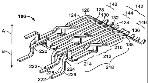
[0027] FIG. 5 illustrates a view of the contact array 106 in
accordance with an embodiment of the present invention. Like item numbers have
been used. First, second and third sections 210, 212 and 214 together form a
main
section 218 which is held generally perpendicular to the circuit board 148. In
a first
section 210, the array contacts 124, 126, 128, 130, 132, 134, 136 and 138
extend
planar to the base 122 (FIG. 3) and normal to the circuit board 148. In a
second
section 212, the pairs of array contacts 124 and 126, 130 and 132, and 136 and
138
cross over each other, while the array contacts 128 and 134 continue planar to
the base
122. The cross-over pattern compensates for a portion of the crosstalk
generated in
the plug. In a third section 214, the array contacts 124, 126, 128, 130, 132,
134, 136
and 138 extend planar to the base 122.
[0028] Each of the array contacts 124, 126, 128, 130, 132, 134, 136
and 138 has a contact tail 216. Each contact tail 216 is bent to form a first
bend 224
of approximately 90 degrees, wherein the array contacts 124, 128, 132 and 136
are
bent in an upward direction as indicated by arrow A and the array contacts
126, 130,
134 and 138 are bent in a downward direction as indicated by arrow B. A first
tail
sub-section 228 extends upwards or downwards, parallel to the circuit board
148 for
one of two distances, and then a second bend 226 of approximately 90 degrees
is
-6-
CA 02646025 2008-09-05
WO 2007/106409 PCT/US2007/006123
formed. A second tail sub-section 222 extends perpendicular to the circuit
board 148
and through one of the contact holes 188, 190, 192, 194, 196, 198, 200 and 202
in the
circuit board 148, forming the contact entry pattern 153 (FIG. 4), which is
discussed
further below.
[0029] FIG. 6 illustrates a side view of the contact array 106 in
accordance with an embodiment of the present invention. First, second, and
third
sections 210, 212, and 214 and contact tails 216 are illustrated with like
item numbers.
Plane 220 illustrates a plane substantially parallel to the plane of the main
section 218,
which is perpendicular to the circuit board 148. The second tail sub-sections
222
extend in four parallel rows formed at distances D1, D2, D3 and D4 from the
plane
220. Distances D1 and D4 are larger than distances D2 and D3. Also, distances
D1
and D4 are equal to each other and distances D2 and D3 are equal to each
other.
[0030] FIG. 7 illustrates a rear perspective view of the sub-assembly
120 of FIG. 3 to better show the contact entry pattern 153 of the second tail
sub-
sections 222. A rear face 152 of the circuit board 148 is shown. The second
tail sub-
sections 222 enter the contact holes 188, 190, 192, 194, 196, 198, 200 and 202
in the
front face 150 and may extend through and beyond the rear face 152 of the
circuit
board 148. The second tail sub-sections 222 may be soldered to the circuit
board 148,
or may be compliant pin, eye of the needle, or other type of connection known
in the
art.
[0031] The spatial relationship of the contact holes 188, 190, 192,
194, 196, 198, 200 and 202 with respect to one another and the spatial
relationship of
the wire termination contact holes 170, 172, 174, 176, 178, 180, 182, and 184
with
respect to one another is determined to achieve a desired electrical
performance. For
example, the contact holes 188, 190, 192, 194, 196, 198, 200 and 202 and wire
termination contact holes 170, 172, 174, 176, 178, 180, 182, and 184 may form
patterns for coupling and isolating certain contacts.
[0032] The wire termination contact pattern 154 will be discussed
first, while the contact entry pattern 153 will be discussed further below. In
the cable
connected to the wire termination contacts 113 of the wire connector housing
112, the
-7-
CA 02646025 2008-09-05
WO 2007/106409 PCT/US2007/006123
two wires of each wire pair are twisted together. In an RJ-45 application, the
wires
are paired as wire pairs 1/2, 3/6, 4/5 and 7/8, which are associated with the
first,
second, third and fourth differential pairs 140, 142, 144 and 146,
respectively. Each
wire pair is received by wire termination contact holes located proximate
different
corners of the board 148. Specifically, wire pair 1/2 is received by wire
termination
contact holes 178 and 180 proximate a first corner, wire pair 3/6 is received
by wire
termination contact holes 170 and 172 proximate a second corner, wire pair 7/8
is
received by wire termination contact holes 182 and 184 proximate a third
corner, and
wire pair 4/5 is received by wire termination contact holes 174 and 176
proximate a
fourth corner.
[0033] The wire termination contact holes 170, 172, 174, 176, 178,
180, 182, and 184 are arranged, in part, to avoid creating additional noise in
the
receptacle assembly 100. As industry standards dictate, the plug contains
sizable
noise with the most noise occurring between the differential pairs 142 and
144.
Because this pair combination has the most noise, the wire termination contact
pattern
154 isolates the wire pairs 3/6 and 4/5 from one another. Referring to FIG. 4,
wire
termination contact holes 170 and 172 accept wire termination contacts 113
interconnected with wire pair 3/6, and wire termination contact holes 174 and
176
accept wire termination contacts 113 interconnected with wire pair 4/5. Wire
termination contact holes 170 and 172 are positioned in one corner of the top
portion
166 while the wire termination contact holes 174 and 176 are positioned in the
opposite corner, respectively, of the bottom portion 168, isolating the second
and third
differential pairs from one another. In other words, the second and third
differential
pairs are located far apart from one another on the circuit board 148.
[0034] The wire termination contact pattern 154 also takes into
consideration the ease of connecting the cable to the receptacle assembly 100.
Two
color schemes determined by industry standards for the RJ-45 are called 568A
and
568B and match pin numbers to wire colors of a cable. Two sets of wire pairs
are
typically designated specific colors, and therefore, within the cable, wire
pair 4/5 is
blue, and wire pair 7/8 is brown. For pattern 568A, wire pair 1/2 is green,
and wire
pair 3/6 is orange. Alternatively, for pattern 568B, wire pair 1/2 is orange
and wire
-8-
CA 02646025 2008-09-05
WO 2007/106409 PCT/US2007/006123
pair 3/6 is green. Another consideration relates to the orientation of the
wires within
the cable jacket. Although not required by the industry, a common wire color
breakout is blue-orange-green-brown that rotates either in the clockwise (CW)
or
counter-clockwise (CCW) direction depending upon which end of the cable is
being
viewed. Therefore, there are four main patterns that may be presented: A-
pattern and
CCW, A-pattern and CW, B-pattern and CCW and B-pattern and CW. The wire
termination contact pattern 154 was chosen so that one of these four main
patterns
matches directly to the jack without the need for altering or crossing over
the wire
pairs within the natural orientation of the cable resulting in ease of
installation where
possible. The pattern chosen for this embodiment was B-pattern and CCW.
[0035] While corresponding to the industry, the wire termination
contact pattern 154 further improves performance by separating noisy pairs.
The wire
pair 4/5 is blue and corresponds to the wire termination contact holes 174 and
176,
and the wire pair 3/6 corresponds to the wire termination contact holes 170
and 172,
which are located in an opposite corner of the board 148 with respect to the
wire
termination contact holes 174 and 176. The wire pair 3/6 may be either green
or
orange. Therefore, in one embodiment, the wire pair 1/2 is orange and
corresponds to
wire termination contact holes 178 and 180, while the wire pair 3/6 is green
and
corresponds to wire termination contact holes 170 and 172. In another
embodiment,
the wire pair 1/2 may be green while the wire pair 3/6 may be orange.
[0036] The contact entry pattern 153 will now be discussed. As
stated previously, in an RJ-45 plug, one of the four differential pairs is
split around
another. Industry standards require a split pair and also dictate how much
noise needs
to occur in the plug. The highest degree of crosstalk is created between these
two
pairs, but the other pair combinations also exhibit crosstalk that is not
insignificant.
This is partly due to the large parallel blades in the plug, and sometimes,
the parallel
nature of the wires as they are dressed into the plug. Therefore, it is
desirable to
counteract this noise in the receptacle assembly 100, such as through
compensation in
the receptacle assembly 100, so the mated connector (the plug and the
receptacle
assembly 100 joined together) has a significantly smaller amount of noise than
the
plug alone.
-9-
CA 02646025 2011-04-01
67789-585
[0037] FIG. 8 illustrates relationships between,and groupings of the
contact holes 188, 190, 192, 194, 196, 198, 200 and 202 within the contact
entry
pattern 153. Each of the contact holes 188, 190, 192, 194, 196, 198, 200 and
202 has
a center 262. Circles and lines are used to show relationships and/or
distances
between the centers 262 of the contact holes 188, 190, 192, 194, 196, 198, 200
and
202, and therefore the circles and lines themselves do not form a part of the
contact
entry pattern 153.
[0038] A first group 230 includes the contact holes 188, 192 and 196
arranged in a triangular layout. A circle 232, which may have a minimum
diameter of
1.02mm (0,04 inch), captures the center 262 of each of the contact holes 188,
192 and
196. In one embodiment, the circle 232 may have a diameter of 2.08mm (.082
inch).
Optionally, the circle 232 may have a diameter of up to 3.56mm (0.140 inch). A
second group 234 includes the contact holes 194, 198 and 202 which are also
arranged
in a triangular layout. A circle 236 captures the center 262 of each of the
contact
holes 194, 198 and 202 and may also have a diameter from 1.02mm to 3.56mm
(0.04
inch to 0.140 inch).
[0039] The contact entry pattern 153 may be further described by
referring again to FIG. 6. The plane 220 has been indicated on FIG. 8. A first
subset
254 includes the contact holes 200, 196 and 188, and the center 262 of each is
the
distance D 1 from the plane 220. A second subset 256 includes contact hole
192, the
center 262 of which is the distance D2 from the plane 220. Third subset 258
includes
contact hole 198, the center 262 of which is the distance D3 from the plane
220.
Fourth subset 260 includes contact holes 202, 194 and 190, and the center 262
of each
is the distance D4 from the plane 220. As stated previously, the distances D1
and D4
are equal to each other and distances D2 and D3 are equal to each other,
[0040] As discussed previously, the eight parallel blades in the plug
experience crosstalk. Regarding second differential pair (blades 3/6) and
third
differential pair (blades 4/5), blades 3 and 4 and blades 5 and 6 have the
greatest level
of noise due to their close proximity with each other. Correspondingly, in the
receptacle assembly 100, the array contacts 128 and 130 and the array contacts
132
-10-
CA 02646025 2011-04-01
67789-585
and 134 experience a higher level of noise due to their close proximity to one
another.
It is desired to isolate the sets of contacts experiencing the higher level of
noise.
Thus, the array contacts 128 and 130 are received by the contact holes 192 and
194,
respectively, which are located away from each other, and the array contacts
132 and
134 are received by contact holes 196 and 198, respectively, which are located
away
from each other. In FIG. 8, line 246 extends between the centers 262 of the
contact
holes 192 and 194 and line 248 extends between the centers 262 of the contact
holes
196 and 198, illustrating a distance between the centers 262 of the respective
contact
holes, which may be from 3.05mm to 5.08mm (0.120 inch to 0.20 inch). In one
embodiment, the distance may be 4.06mm (0.160 inch).
[0041] The noise in the receptacle assembly 100 may be further
counteracted through compensation by placing other array contacts close to one
another. The array contacts 128 and 132 are received by contact holes 192 and
196,
respectively, which are located in close proximity to each other, and the
array contacts
130 and 134 are received by contact holes 194 and 198, respectively, which are
located in close proximity to each other. In FIG. 8, line 238 extends between
the
centers 262 of the contact holes 192 and 196 and line 240 extends between the
centers
262 of the contact holes 194 and 198, illustrating a distance between the
centers of the
respective contact holes 262 which may be from 0.51mm to 2.54mm (0.02 inch to
0.100 inch). In one embodiment, the distance may be 1.63mm (0.064 inch).
[0042] Three of the differential pairs experience a secondary level of
noise, or second tier of crosstalk, in the plug. The second differential pair
(blades 3/6)
experiences a high level of noise with both the first differential pair
(blades 1/2) and
fourth differential pair (blades 7/8) due to their proximity in the plug and
because the
second differential pair is a split pair.
[0043] To isolate signals experiencing a high level of noise, the array
contacts 126 and 128 are received by contact holes 190 and 192, respectively,
which
are located away from each other, and array contacts 134 and 136 are received
by
contact holes 198 and 200, respectively, which are located away from each
other. In
FIG. 8, line 250 extends between the centers 262 of the contact holes 190 and
192 and
- 11 -
CA 02646025 2011-04-01
67789-585
line 252 extends between the centers 262 of the contact holes 198 and 200,
illustrating
a distance between the centers 262 of the respective contact holes, which may
be from
3.05mm to 5.08mm (0.120 inch to 0.20 inch). Similarly, to couple signals to
counteract the crosstalk occurring in the RJ-45 plug, contact holes 188 and
192
receiving array contacts 124 and 128, respectively, and contact holes 198 and
202
receiving array contacts 134 and 138, respectively, are placed in closer
proximity to
one another on the circuit board 148. In FIG. 8, line 242 extends between the
centers
262 of the contact holes 188 and 192 and line 244 extends between the centers
262 of
the contact holes 198 and 202, illustrating a distance between the centers 262
of the
respective contact holes, which may be from 0.51mm to 2.54mm (0.02 inch to
0.100
inch).
[0044] Return loss which occurs throughout the jack and the
receptacle assembly 100 is also considered. A signal sent down two pins (or
contacts
or wires) in a differential pair has an impedance based on at least one of
cross-section
of the conductor, space between the conductors and the dielectric constant
separating
the two conductors in a pair. The adjacent array contacts of the first, third
and fourth
differential pairs 140, 144 and 146 have essentially the same geometry, and
are close
together in the receptacle assembly 100, resulting in an impedance between the
array
contacts of each pair that is lower than desired. By increasing the impedance
to match
the target impedance, such as 100 ohms, the return loss is improved.
Therefore,
contact holes 200 and 202 receiving array contacts 136 and 138, respectively,
of the
fourth differential pair, are placed farther apart with respect to each other,
as are
contact holes 188 and 190 receiving array contacts 124 and 126, respectively,
of the
first differential pair, and contact holes 194 and 196 receiving array
contacts 130 and
132, respectively, of the third differential pair. Distance between the
contact holes of
a differential pair may be increased to increase the impedance, providing a
more
favorable return loss.
[0045] While the invention has been described in terms of various
specific embodiments, those skilled in the art will recognize that the
invention can be
practiced with modification within the scope of the claims.
-12-