Note: Descriptions are shown in the official language in which they were submitted.
CA 02646325 2008-09-17
WO 2007/109231 PCT/US2007/006814
SPINTRONIC DEVICES WITH CONSTRAINED
SPINTRONIC DOPANT AND ASSOCIATED METHODS
Field of the Invention
[0001] The present invention relates to the field of
electronics, and, more particularly, to the field of spin-
based electronics and associated methods.
Background of the Invention
[0002] Spin-based electronics or spintronics exploit
both the charge of electrons as well as the spin of the
electrons to permit new devices with enhanced functions,
higher speeds, and/or reduced.power consumption, for
example. An exemplary spintronic device is the spin valve
as illustrated in the FIGS. 1A and 1B. The spin valve 11
provides a low resistance when the spins are aligned (FIG.
1A), and provides a high resistance with the spins not
aligned (FIG. 1B). The spin valve 11 may be used as a
nonvolatile memory element, for example. Other exemplary
spintronic devices including the spin-FET 12 schematically
illustrated in FIG. 2, and the quantum bit device 13
illustrated in FIG. 3.
[0003] Published U.S. Patent Application No.
2006/0018816, for example, discloses a Diluted Magnetic
Semiconductor (DMS) comprising zinc oxide which includes a
transition element or a rare earth lanthanide, or both, in
an amount sufficient to change the material from non-
magnetic state to a room temperature ferromagnetic state.
The material may be in a bulk form or a thin film form. A
DMS material is a semiconductor in which transition metal
1
CA 02646325 2008-09-17
WO 2007/109231 PCT/US2007/006814
ions or rare earth lanthanides substitute cations of host
semiconductor materials. More particularly, a DMS material
15 is schematically illustrated in FIG. 4B, while to the
left in FIG. 4A is a magnetic material 14, and to the right
in FIG. 4C is a non-magnetic material 16.
[0004] Published U.S. Patent Application No.
2005/0258416 discloses a spintronic switching device
comprising a half-metal region between first and second
conductive regions. The half-metal region comprises a
material that, at the intrinsic Fermi level, has
substantially zero available electronic states in a
minority spin channel. Changing the voltage of the half-
metal region with respect to the first conducting region
moves its Fermi level with respect to the electron energy
bands of the first conducting region, which changes the
number of available electronic states in the majority spin
channel. In doing so, this changes the majority spin
polarized current passing through the switching device.
The half-metal region may comprise CrAs and the conducting
regions may comprise a p-doped or n-doped semiconductor.
For example, the p-doped semiconductor may comprise Mn
doped GaAs.
[0005] Published U.S. Patent Application No.
2004/0178460 discloses a spintronic device application as a
memory and a logic device using a spin valve effect
obtained by injecting a carrier spin-polarized from a
ferromagnetic into a semiconductor at room temperature, and
a spin-polarized field effect transistor. The ferromagnet
is disclosed as one of a Fe, Co, Ni, FeCo, NiFe, GaMnAs,
InMnAs, GeMn, and GaMnN, and can be a half metal having a
spin polarization of 100% such as Cr02. The semiconductor
may be one selected from Si, GaAs, InAs, and Ge. Also, the
2
CA 02646325 2008-09-17
WO 2007/109231 PCT/US2007/006814
spin channel region is disclosed as Si on insulator (SOI)
or a two-dimensional electron gas of a compound
semiconductor.
[0006] An article to Jonker et al. "Electrical Spin
Injection and Transport in Semiconductor Spintronic
Devices", MRS Bulletin/Oct. 2003, pp. 740-748, discloses
semiconductor heterostructures that use carrier spin as a
new degree of freedom. The article discloses four
essential requirements for implementing a semiconductor
spintronics technology in devices, and provides that the
efficient electrical injection of spin-polarized carriers
into the semiconductor has been a critical issue severely
hampering progress in this field. The article further
discloses that advances in materials quality have increased
the Curie temperature of Gal_xMn,As to -150 K with the
potential of exceeding room temperature. Spin-dependent
resonant tunneling is identified as able to increase the
spin selectivity of tunneling contacts in a very efficient
way. A double-barrier heterojunction (DBH) comprising a
nonmagnetic semiconductor quantum well between two
insulating barriers and two ferromagnetic semiconductive
electrodes may behave as half-metallic junctions if the
parameters of the quantum well and barrier are properly
tuned.
[0007] Current spintronics technology is limited by the
currently used materials. For example, it is important, as
noted by Jonker et al., to have efficient spin carrier
injection. It is also desirable to have manufacturing and
operational compatibility with existing semiconductor
processing technology. It is also desirable that the
magnetic ordering or Curie temperature by at or near room
temperature, instead of the more typical 100-200 K. One
3
CA 02646325 2008-09-17
WO 2007/109231 PCT/US2007/006814
potential approach is the DMS materials as disclosed in the
above noted U.S. Patent Application No. 2004/0178460.
[0008] Another spintronic device structure is the
Digital Ferromagnetic Heterostructure (DFH) as disclosed,
for example, by Sanvito et al. in an article "Ab Initio
Transport Theory for Digital Ferromagnetic
Heterostructures" in Physical Review Letters, Vol. 87, No.
26, December 24, 2001, pp. 1-4. The article notes that the
solubility limit of Mn in GaAs is rather small; however, a
large MN concentration can be obtained in a zinc blende
MnAs submonolayers into GaAs to form a MnAs/GaAs
superlattice. A schematic diagram of a prior art DFH
structure 18 is shown in FIG. 5 with a transition metal
(Tm) in the form of Mn within a Silicon superlattice.
Although this may have a large spin polarization at the
Fermi level and a large magnetoresistance effect and Curie
temperature higher than in the bulk, it may suffer from a
low thermal stability.
[0009] Unfortunately, many of the materials and
structures for spintronic devices have relatively low
concentrations of the spintronic dopant, such as Mn. The
spintronic dopant tends to precipitate out of the.crystal
lattice, especially as the concentration is increased,
and/or the device is subjected to thermal processing steps.
Summary of the Invention
[0010] In view of the foregoing background, it is
therefore an object of the present invention to provide a
spintronic device that is readily manufactured and which
exhibits good spintronic characteristics, such as at room
temperature or higher, for example.
4
CA 02646325 2008-09-17
WO 2007/109231 PCT/US2007/006814
[0011] This and other objects, features and advantages
in accordance with the present invention are provided by a
spintronic device comprising at least one superlattice and
at least one electrical contact coupled thereto, with the
at least one superlattice comprising a plurality of groups
of layers. Each group of layers may comprise a plurality
of stacked base semiconductor monolayers defining a base
semiconductor portion having a crystal lattice, at least
one non-semiconductor monolayer constrained within the
crystal lattice of adjacent base semiconductor portions,
and a spintronic dopant. Moreover, the spintronic dopant
may be constrained within the crystal lattice of the base
semiconductor portion by the at least one non-semiconductor
monolayer. Accordingly, a fairly high spintronic dopant
concentration may be achieved and maintained while reducing
a likelihood of precipitation of the spintronic dopant.
[0012] The spintronic dopant may comprise at least one
spintronic dopant monolayer=adjacent the at least one non-
semiconductor monolayer. This may be so, for example,
where the energy levels favor attraction and retention of
the spintronic dopant to the non-semiconductor. The
spintronic dopant may comprises a transition metal, such as
at least one of Manganese, Iron, and Chromium.
Alternatively or additionally the spintronic dopant may
comprise a rare earth, such as a rare earth lanthanide, for
example.
[0013] The non-semiconductor may comprise at least one
of Oxygen, Nitrogen, Fluorine, Carbon-Oxygen, and Sulphur,
for example. The semiconductor may comprise Silicon, or
more generally, may comprise a semiconductor selected from
the group comprising Group IV semiconductors, Group III-V
semiconductors, and Group II-VI semiconductors. The
CA 02646325 2008-09-17
WO 2007/109231 PCT/US2007/006814
specific materials and structural configurations may be
preferably selected so that the superlattice exhibits a
Curie temperature of at least as high as room temperature.
[0014] An embodiment of the spintronic device may be a
spintronic field effect transistor. Accordingly, the
spintronic FET may include a substrate carrying a pair of
superlattices in spaced apart relation to define a source
and a drain, with a channel between the source and drain,
and a gate adjacent the channel. Another embodiment of the
spintronic device is a spin valve. The spin valve may also
include a substrate carrying a pair of superlattices in
spaced apart relation with a spacer between the pair of
superlattices.
[0015] In some embodiments the repeating structure of a
superlattice may not be needed. In other words, the
spintronic device may comprise a plurality of stacked base
semiconductor monolayers defining a base semiconductor
portion having a crystal lattice, at least one non-
semiconductor monolayer constrained within the crystal
lattice, and a spintronic dopant constrained within the
crystal lattice of the base semiconductor portion by the at
least one non-semiconductor monolayer. In addition, the
device may also include an electrical contact coupled to
the base semiconductor portion.
[0016] A method aspect is for making a spintronic device
comprising forming at least one superlattice and forming at
least one electrical contact coupled thereto, with the at
least one superlattice comprising a plurality of groups of
layers. Each group of layers may comprise a plurality of
stacked base-semiconductor monolayers defining a base
semiconductor portion having a crystal lattice, at least
one non-semiconductor monolayer constrained within the
6
CA 02646325 2008-09-17
WO 2007/109231 PCT/US2007/006814
crystal lattice of adjacent base semiconductor portions,
and a spintronic dopant. Moreover, the spintronic dopant
may be constrained within the crystal lattice of the base
semiconductor portion by the at least one non-semiconductor
monolayer. Other method aspects will also be understood by
those skilled in the art based on the teachings herein.
Brief Description of the Drawings
[0017] FIG. lA is a schematic diagram of a spin valve as
is in the prior art illustrated in a low resistance state.
[0018] FIG. 1B is a schematic diagram of the prior art
spin valve as shown in FIG. 1A illustrated in a high
resistance state.
[0019] FIG. 2 is a schematic perspective view of a spin
FET as in the prior art.
[0020] FIG. 3 is a schematic diagram of a quantum bit
device as in the prior art.
[0021] FIG. 4A is a schematic diagram of a magnetic
material as in the prior art.
[0022] FIG. 4B is a schematic diagram of a dilute
magnetic material as in the prior art.
[0023] FIG. 4C is a schematic diagram of a non-magnetic
material as in the prior art.
[0024] FIG. 5 is a schematic atomic diagram for a
Digital Ferromagnetic Heterostructure (DFH) as in the prior
art.
[0025] FIGS. 6A and 6B are, respectively, a schematic
diagram and energy level diagram for a DFH in accordance
with the invention.
[0026] FIG. 7 is a schematic atomic diagram for a DFH
structure in accordance with the invention.
7
CA 02646325 2008-09-17
WO 2007/109231 PCT/US2007/006814
[0027] FIG. 8 is a schematic atomic model of a portion
of a superlattice for a spintronic device in accordance
with the present invention.
[0028] FIG. 9 is a combined energy diagram for the
superlattice as shown in FIG. 8.
[0029] FIGS. 10A-10C are schematic atomic diagrams of
various relative atomic positions of Si, 0, and Mn in a
spintronic device in accordance with the invention.
[0030] FIG. 11 is a schematic cross-sectional diagram of
a spintronic FET in accordance with the invention.
[0031] FIG. 12 is a schematic cross-sectional diagram of
a spin valve in accordance with the invention.
Detailed Description of the Preferred Embodiments
[0032] The present invention will now be described more
fully hereinafter with reference to the accompanying
drawings, in which preferred embodiments of the invention
are shown. This invention may, however, be embodied in many
different forms and should not be construed as limited to
the embodiments set forth herein. Rather, these embodiments
are provided so that this disclosure will be thorough and
complete, and will fully convey the scope of the invention
to those skilled in the art. Like numbers refer, to like
elements throughout.
[0033] Referring now to FIGS. 6A and 6B, a first example
of the present invention is now described. In the
schematically illustrated DFH structure 20 of FIG. 6A,
Oxygen is included in the Si superlattice also including a
transition metal, such as Mn. As can be seen in the energy
level diagram 21 of FIG. 6B, the Mn will have lower energy
as it approaches the Oxygen layer. In other words, when
the Mn atoms stick to the Silicon atoms, the structure is
most energetically favorable, and the Mn atoms can be well
8
CA 02646325 2008-09-17
WO 2007/109231 PCT/US2007/006814
positioned and confined in the Silicon. As will be
appreciated by those skilled in the art, the relative
positioning of the Mn atoms with respect to the Oxygen
atoms may be used to tune the Curie temperature (Tc), for
example. The Tc may be much higher than room temperature
for a 2D confined system, for example. The DFH structure
20 with Oxygen i.s advantageously more thermally stable than
prior art structures.
[0034] Mn, for example, substitutionally introduces only
a small stress into the Silicon monocrystalline structure.
Mn is an example of a transition metal suitable for
spintronic devices. Those of skill in the art will
appreciate that other materials may be used as well, such
as, for example, Fe, Cr, etc. Rare earth elements may also
be used, such as rare earth lanthanides.
[0035] Other materials may also be used in place of or
in combination with Oxygen. For example, Nitrogen,
Fluorine, Carbon-Oxygen, and Sulphur are suitable
materials. In addition, the base semiconductor
illustratively in the form of Si, may be a'semiconductor
selected from the group comprising Group IV semiconductors,
Group III-V semiconductors, and Group II-VI semiconductors.
Of course, and the term Group IV semiconductors also
includes Group IV-IV semiconductors.
[0036] The charge and spin densities of various layers
of a DFH structure 22 and incorporating Oxygen along with
Mn in an Si monocrystalline superlattice is schematically
illustrated in FIG. 7. Layer 1 is shown to be in a
conductive state, in contrast to the other layers, Layers 6
and 16.
[0037] A schematic atomic model 25 is shown in FIG. 8,
with the transition metal (e.g. Mn) incorporated in the
9
CA 02646325 2008-09-17
WO 2007/109231 PCT/US2007/006814
Silicon lattice along with Oxygen. With reference to FIG.
9, the spin-up energy states 27 (top) and the spin-down
energy states 28 (bottom) are shown. The spin-up energy
diagram 27 indicates that current will flow because of the
low energy states at the Fermi level as will be appreciated
by those skilled in the art, and in contrast to the high
energy states at the Fermi level for the spin-down diagram
28.
[0038] Referring now additionally to FIGS. 10A-10C the
relative energetics of various Si-Mn-O structures are
schematically illustrated. More particularly, the
structure 31 shown in FIG. 10A with an Oxygen atom between
adjacent Mn atoms offers the lowest stability, the
structure 32 shown in FIG. lOB with an Oxygen atom remote
from a pair of Mn atoms offers an intermediate stability,
and the structure 33 shown in FIG. lOC with an Oxygen atom
tied to one of a pair of Mn atoms offers the highest
relative stability.
[0039] In some embodiments, the spintronic device may
comprise at least one superlattice and at least one
electrical contact coupled thereto, with the at least one
superlattice comprising a plurality of groups of layers.
Each group of layers may comprise a plurality of stacked
base semiconductor monolayers defining a base semiconductor
portion having a crystal lattice, at least one non-
semiconductor monolayer constrained within the crystal
lattice of adjacent base semiconductor portions, and a
spintronic dopant. The base semiconductor portion may
comprise 5 o 30 monolayers, for example. The spintronic
dopant may be constrained within the crystal lattice of the
base semiconductor portion by the at least one non-
semiconductor monolayer as described above. Accordingly, a
CA 02646325 2008-09-17
WO 2007/109231 PCT/US2007/006814
relatively high spintronic dopant concentration may be
achieved and maintained while reducing a likelihood of
precipitation of the spintronic dopant. For example, the
concentration of the spintronic dopant may be in the range
of from about 0.1 to 10 percent.
[0040] The spintronic dopant may comprise at least one
spintronic dopant monolayer adjacent the at least one non-
semiconductor nionolayer. This may be so, for example,
where the energy levels favor attraction and retention of
the spintronic dopant to the non-semiconductor.
[0041] Further details regarding superlattice structures
including Silicon and Oxygen to achieve energy band
modifications, such as to increase charge carrier mobility,
are described in commonly assigned U.S. Patent Nos.
6,891,188 and 7,153,763, for example, the entire contents
of which are incorporated herein by reference. In
accordance with the spintronic devices described herein,
Applicants theorize without wishing to be bound thereto
that the non-semiconductor monolayer(s) may serve to
collect or at least contain the spintronic dopant to keep
the dopant from precipitating out, especially during any
subsequent thermal processing steps as will be appreciated
by those skilled in the art. In some embodiments, the
spintronic dopant may be added by atomic layer deposition.
In other embodiments, the spintronic dopant may be added by
implantation and optionally followed by an anneal, for
example, while the non-semiconductor monolayer(s) serves to
at least contain the dopant.
[0042] The non-semiconductor monolayer may be initially
formed in a non-continuous fashion, that is, without all
available positions for Oxygen being filled in the Silicon
lattice, for example. Moreover, Applicants also theorize
11
CA 02646325 2008-09-17
WO 2007/109231 PCT/US2007/006814
without wishing to be bound thereto that Atomic Layer
Deposition (ALD) of the monolayers may tend to form
clusters on an atomic level rather than clearly or
precisely defined moriolayers, especially when subjected to
subsequent thermal processes. For example, the
superlattices in some cases may be formed before shallow
trench isolation (STI) formation, and are thus subjected to
thermal processing during STI formation.
[0043] Accordingly, the term monolayer is intended to
cover this theorized clustering phenomenon, and is not
limited to a precise mathematical or atomic stick model
layer as will be appreciated by those skilled in the art.
It is also theorized by Applicants without their wishing to
be bound thereto, that a clustering phenomenon may be
considered to occur with the spintronic dopant, especially
for the those combinations of materials, such as Si-O-Mn,
where the Mn will be attracted to the 0.
[0044] Extending the principles described herein
further, in some embodiments the repeating structure of a
superlattice may not be needed. In other words, the
spintronic device may comprise a plurality of stacked base
semiconductor monolayers defining a base semiconductor
portion having a crystal lattice, at least one non-
semiconductor monolayer constrained within the crystal
lattice, and a spintronic dopant constrained within the
crystal lattice of the base semiconductor portion by the at
least one non-semiconductor monolayer. The device may also
include an electrical contact coupled to the base
semiconductor portion.
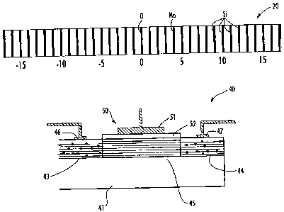
[0045] Referring now additionally to FIG. 11, an example
of a spintronic device in the form of a spintronic field
effect transistor (FET) 40 is now described. The
12
CA 02646325 2008-09-17
WO 2007/109231 PCT/US2007/006814
spintronic FET 40 illustratively includes a semiconductor
substrate 41 carrying a pair of superlattices in spaced
apart relation to define a source*43 and a drain 44, with a
channel 45 between the source and drain, and a gate 50
adjacent the channel. The gate 50 includes a dielectric
layer 52 and a gate electrode or contact 51 thereon.
[0046] For clarity of explanation the source 43 and
drain 44 are illustrated with a plurality of horizontally
extending lines schematically indicating the repeating
groups of the superlattice and with dots indicative of the
spintronic dopant. A source contact 46 and a drain contact
47 are illustratively coupled to the source 43 and drain 44
respectively. The channel 45 is illustratively in the form
of a superlattice as well, but without the spintronic
dopant. In other embodiments, the channel need not be a
superlattice as will be appreciated by those skilled in the
art. In yet other embodiments, only one of the source or
drain may be a superlattice.
[0047] Another embodiment of a spintronic device is the
spin valve 60 explained with additional reference to FIG.
12. The spin valve 60 also includes a semiconductor
substrate 61 that carries on its upper surface a pair of
superlatices 62, 63 in spaced apart relation with a spacer
66 between the pair of superlattices. Respective
electrical contacts 64, 65 are coupled to the superlattices
64, 65. As will be appreciated by those skilled in the
art, one of the superlattices 64, 65 may be constructed to
be pinned or be a hard ferromagnetic region, while the
other is a soft ferromagnetic region.
[0048] A method aspect is for making a spintronic device
comprising forming at least one superlattice and forming at
least one electrical contact coupled thereto, with the at
13
CA 02646325 2008-09-17
WO 2007/109231 PCT/US2007/006814
least one superlattice comprising a plurality of groups of
layers. Each group of layers may comprise a plurality of
stacked base semiconductor monolayers defining a base
semiconductor portion having a crystal lattice, at least
one non-semiconductor monolayer constrained within the
crystal lattice of adjacent base semiconductor portions,
and a spintronic dopant. Moreover, the spintronic dopant
may be constrained within the crystal lattice of the base
semiconductor portion by the at least one non-semiconductor
monolayer. Other method aspects will also be understood by
those skilled in the art based on the teachings herein.
[0049] The spintronic devices described herein,
including the spintronic FET and spin valve, may also be
configured without the repeating structure of the
superlattice as will be appreciated by those of skill in
the art. The materials described herein may be used in
many spintronic devices, particularly for increasing the
injection efficiency of =spin carriers believed due to the
material compatibility at the interface. The thermal
stability of the devices may also be greatly enhanced
believed due to the Oxygen being held in the crystal
lattice, and the Mn being thermally stable adjacent the
Oxygen atoms. Other general references in the field of
spintronics include an article by Park et al. appearing in
Science 295, 651 (2002); an article to Qian et al. in Phys.
Rev. Lett. 96, 027211 (2006); and an article to Ohno et al.
appearing in Nature 402, 790 (1999).
[0050] In addition, many modifications and other
embodiments of the invention will come to the mind of one
skilled in the art having the benefit of the teachings
presented in the foregoing descriptions and the associated
drawings. Therefore, it is understood that the invention is
14
CA 02646325 2008-09-17
WO 2007/109231 PCT/US2007/006814
not to be limited to the specific embodiments disclosed,
and that modifications and embodiments are intended to be
included within the scope of the invention.