Note: Descriptions are shown in the official language in which they were submitted.
CA 02646367 2010-03-18
LOW THRESHOLD VOLTAGE ANTI-FUSE DEVICE
FIELD OF THE INVENTION
[0001] The present invention relates generally to non-volatile memory. More
particularly, the present invention relates to anti-fuse devices.
BACKGROUND OF THE INVENTION
[0002] In the following description the term MOS is used to denote any FET or
MIS
transistor, half-transistor or capacitor structure. In order to simplify the
description of the
embodiments, references to gate oxides from this point forward should be
understood to
include dielectric materials, oxide, or a combination of oxide and dielectric
materials.
[0003] Over the past 30 years, anti-fuse technology has attracted significant
attention
of many inventors, IC designers and manufacturers. An anti-fuse is a structure
alterable to a
conductive state, or in other words, an electronic device that changes state
from not
conducting to conducting. Equivalently, the binary states can be either one of
high resistance
and low resistance in response to electric stress, such as a programming
voltage or current.
Anti-fuse devices can be arranged into a memory array, thereby forming what is
commonly
known as a one-time-programmable (OTP) memory.
[0004] Current anti-fuse development is concentrated around 3-dimensional thin
film
structures and special inter-metal materials. Such anti-fuse technologies
require additional
processing steps not available in standard CMOS process, prohibiting anti-fuse
applications
in typical VLSI and ASIC designs, where programmability could help overcome
problems
with ever shrinking device life cycles and constantly rising chip development
costs. Therefore
there is an apparent need in the industry for a reliable anti-fuse structures
utilizing standard
CMOS process.
-1-
CA 02646367 2008-12-23
[0006] One type of anti-fuse memory cell manufacturable with a standard CMOS
process is disclosed in U.S. Pat. No. 6,667,902 (Peng). Peng attempts to
improve a classic
planar DRAM-like anti-fuse array by introducing "row program lines" which
connect to the
capacitors and run parallel to the word lines. If decoded, the row program
lines can minimize
exposure of access transistors to a high programming voltage, which would
otherwise occur
through already programmed cells. Peng further improves his array in U.S. Pat.
No.
6,671,040 by adding a variable voltage controlling programming current, which
allegedly
controls the degree of gate oxide breakdown, allowing for multilevel or analog
storage
applications.
[0007] Figure 1 is a circuit diagram of an anti-fuse memory cell disclosed in
Peng,
while Figures 2 and 3 show the planar and cross-sectional views respectively
of the anti-fuse
memory cell shown in Figure 1. The anti-fuse memory cell of Figure 1 includes
a pass, or
access transistor 10 for coupling a bitline BL to a bottom plate of anti-fuse
device 12. Anti-
fuse device 12 is considered a gate dielectric breakdown based anti-fuse
devices. A wordline
WL is coupled to the gate of access transistor 10 to turn it on, and a cell
plate voltage Vcp is
coupled to the top plate of anti-fuse device 12 for programming anti-fuse
device 12.
[0008] It can be seen from Figures 2 and 3 that the layout of access
transistor 10 and
anti-fuse device 12 is very straight-forward and simple. The gate 14 of access
transistor 10
and the top plate 16 of anti-fuse device 12 are constructed with the same
layer of polysilicon,
which extend across active area 18. In the active area 18 underneath each
polysilicon layer,
is formed a thin gate oxide 20, also known as a gate dielectric, for
electrically isolating the
polysilicon from the active area underneath. On either side of gate 14 are
diffusion regions
22 and 24, where diffusion region 24 is coupled to a bitline. Although not
shown, those of skill
in the art will understand that standard CMOS processing, such as sidewall
spacer formation,
lightly doped diffusions (LDD) and diffusion and gate silicidation, can be
applied. While the
classical single transistor and capacitor cell configuration is widely used, a
transistor-only
anti-fuse cell is further desirable due to the semiconductor array area
savings that can be
obtained for high-density applications. Such transistor-only anti-fuses should
be reliable while
simple to manufacture with a low cost CMOS process.
[0009] The gate dielectric breakdown based antifuse devices are gaining
popularity
as a preferred OTP or emulated multiple time programmable (MTP) non-volatile
memory
devices in the industry. Such antifuse devices used either in a memory array
or as an
-2-
CA 02646367 2009-11-13
individual programmable cell consists of at least two regions. First is a high
voltage
breakdown region and second is a low voltage breakdown region (or anti-fuse
region).
[0009] Figure 4 is a cross sectional diagram of an improved version of the
anti-fuse
memory cell shown in Figure 1. Just like the anti-fuse memory cell of Figure
1, Figure 4
shows a two-transistor anti-fuse memory cell 30, which consists of an access
transistor in
series with an anti-fuse transistor. The access transistor includes a
polysilicon gate 32
overlying a thick gate oxide 34, which itself is formed over the channel 36.
On the left side of
the channel 36 is a diffusion region 38 electrically connected to a bitline
contact 40. On the
right side of the channel 36 is a common diffusion region 42 shared with the
anti-fuse
transistor. The anti-fuse transistor includes a polysilicon gate 44 overlying
a thin gate oxide
46, which itself is formed over the channel 48. The thick gate oxide 34 can
correspond to that
used for high voltage transistors while the thin gate oxide 46 can correspond
to that used for
low voltage transistors. Polysilicon gates 32 and 44 can be independently
controlled, or
alternatively can be connected to each other. For example, polysilicon gate 32
can be
coupled to a wordline while polysilicon gate 44 can be coupled to a controlled
cell plate
voltage (VCP). Both diffusion regions 38 and 42 can have LDD regions, which
can be
identically doped or differently doped, depending on the desired operating
voltages to be
used. Thick field oxide, or shallow trench isolation (STI) oxide 54 and 56 are
formed for
isolating the memory cell from other memory cells and/or core circuitry
transistors.
Commonly owned U.S. Patent Publication No. 2007/0257331 filed on June 13, 2007
describes alternate two-transistor anti-fuse memory cells which can be used in
a non-volatile
memory array. The thin gate oxide 46 is intended to breakdown in the presence
of a large
electrical field during a programming operation, thereby creating an
electrically conductive
connection between channel 48 and polysilicon gate 44. This electrically
conductive
connection can be referred to as a conductive link or anti-fuse.
[0010] Such an anti-fuse device implemented in a standard CMOS process
utilizes
high voltage (HV) or input/output (I/O) transistors and low voltage (LV) or
core transistors to
implement the thick dielectric and thin dielectric regions respectively. The
fabrication of HV
and LV transistors includes the process steps such as well formation and
threshold voltage
(Vt) adjustment implants. Those skilled in the art will understand that HV
transistors are
typically used in the I/O circuits such as input and output buffers, or in the
circuitry that
requires lower leakage and/or higher operating voltage comparing to the core
area, where
-3-
CA 02646367 2008-12-23
the LV transistors can be used. LV transistors on the other hand are typically
used for core
circuit transistors, or for circuitry that requires high speed switching
performance for example.
Accordingly, the electrical characteristics of HV and LV transistors are
different since they
are designed for specific applications. In the two-transistor anti-fuse memory
cell 30, it is
desirable to minimize the Vt of the anti-fuse device consisting of polysilicon
gate 44.
Therefore it is formed using an LV transistor process. As shown in Figure 4 by
example, the
anti-fuse device consisting of polysilicon gate 44 is formed in a low voltage
p-type well
(PWELL-LV) 50 that has a dopant concentration, a Vt implant and gate oxide
thickness
specifically set for an LV transistor. The pass gate consisting of polysilicon
gate 32 is formed
in a high voltage p-type well (PWELL-HV) 52 that has a dopant concentration, a
Vt implant
and a gate oxide thickness specifically set for an HV transistor. Therefore
the Vt of the anti-
fuse device will be the same as the Vt of a core circuit transistor.
[0012] A driving factor for reducing cost of any memory is the memory array
area.
The two-transistor anti-fuse memory cell 30 of Figure 4 is a relatively large
memory cell when
compared to single transistor memory cells, such as flash memory cells for
example. A single
transistor anti-fuse memory cell is described in commonly owned U.S. Patent
No. 7,402,855.
[0013] Figure 5 is a cross-sectional view of the single transistor anti-fuse
memory cell
disclosed in commonly owned U.S. Patent No. 7,402,855. Anti-fuse transistor 60
includes a
variable thickness gate oxide 62 formed on the substrate channel region 64, a
polysilicon
gate 66, sidewall spacers 68, a field oxide region 70 a diffusion region 72,
and an LDD region
74 in the diffusion region 72. A bitline contact 76 is shown to be in
electrical contact with
diffusion region 72. The variable thickness gate oxide 62 consists of a thick
gate oxide and a
thin gate oxide such that a portion of the channel length is covered by the
thick gate oxide
and the remaining portion of the channel length is covered by the thin gate
oxide. From this
point forward, the thin gate oxide portion corresponds to the anti-fuse device
portion of the
single transistor anti-fuse memory cell while the thick gate oxide portion
corresponds to the
access transistor portion of the single transistor anti-fuse memory cell.
Generally, the thin
gate oxide is a region where oxide breakdown can occur. The thick gate oxide
edge meeting
diffusion region 72 on the other hand, defines an access edge where gate oxide
breakdown
is prevented and current between the gate 66 and diffusion region 72 is to
flow for a
programmed anti-fuse transistor. While the distance that the thick oxide
portion extends into
the channel region depends on the mask grade, the thick oxide portion is
preferably formed
-4-
CA 02646367 2008-12-23
to be at least as long as the minimum length of a high voltage transistor
formed on the same
chip.
[0014] In the presently shown example, the diffusion region 72 is connected to
a
bitline through a bitline contact 76, or other line for sensing a current from
the polysilicon gate
66, and can be doped to accommodate programming voltages or currents. This
diffusion
region 72 is formed proximate to the thick oxide portion of the variable
thickness gate oxide
62. To further protect the edge of anti-fuse transistor 60 from high voltage
damage, or current
leakage, a resistor protection oxide (RPO), also known as a salicide protect
oxide, can be
introduced during the fabrication process to further space metal particles
from the edge of
sidewall spacer 68. This RPO is preferably used during the salicidation
process for
preventing only a portion of diffusion region 72 and a portion of polysilicon
gate 66 from
being salicided. It is well known that salicided transistors are known to have
higher leakage
and therefore lower breakdown voltage. Thus having a non-salicided diffusion
region 72 will
reduce leakage. Diffusion region 72 can be doped for low voltage transistors
or high voltage
transistors or a combination of the two resulting in same or different
diffusion profiles.
[0015] Once again, it is desirable to minimize the Vt of the anti-fuse device
defined by
the portion of the polysilicon gate 66 over the thin gate oxide portion of the
variable thickness
gate oxide 62. Therefore it is formed using an LV transistor process. As shown
in Figure 5 by
example, the anti-fuse device consisting of polysilicon gate 66 over the thin
gate oxide
portion is formed in a low voltage p-type well PWELL-LV 78 that has a dopant
concentration,
a Vt implant and gate oxide thickness specifically set for an LV transistor.
The pass gate
consisting of polysilicon gate 66 over the thick gate oxide portion of the
variable thickness
gate oxide 62 is formed in a high voltage p-type well PWELL-HV 80 that has a
dopant
concentration, a Vt implant and a gate oxide thickness specifically set for an
HV transistor.
Therefore the Vt of the anti-fuse device will be the same as the Vt of a core
circuit transistor.
[0016] Unfortunately, foundries for manufacturing semiconductor devices may
have
set types of LV transistor processes for manufacturing core circuits of the
memory device,
where the Vt control implant differs depending on the circuit application or
function.
Semiconductor memory devices generally have three circuit areas. First are the
I/O circuits
that are connected to pins of the package of the semiconductor memory device.
Second are
the core circuits, which includes any logic and control circuits for example.
Third is the
memory array, which includes memory cells. Compounding this problem is the
fact that the
-5-
CA 02646367 2008-12-23
anti-fuse is typically designed on the basis of a particular LV transistor
process, which means
that the anti-fuse device has been qualified to operate properly if
manufactured according to
that particular LV transistor process. If the foundry does not have an LV
transistor process
suited for the design, then redesign of the anti-fuse device is required in
order to qualify it for
the available process. Such redesign incurs significant cost overhead, which
is necessitated
again when the foundry introduces a new generation of the process to
accommodate a new
manufacturing technology node. For example, an LV process for a 45nm
technology node
may be different than that of a 20nm technology node.
[0017] Another problem relevant to the anti-fuse transistor 60 of Figure 5 is
mask
alignment error associated with implantation of wells 78 and 80. Because the
thin gate oxide
portion of the variable thickness gate oxide 66 is small, any mask alignment
error becomes
significant. This means that too much of well 78 can be formed under the thick
gate oxide
portion, or too little of well 78 can be formed under the thin gate oxide
portion. In either case,
defects affecting the proper operation of the single transistor anti-fuse
memory cell are more
likely to be formed.
[0018] Another important issue is reliability of the anti-fuse memory device,
and more
specifically the quality of the thin gate oxide. The thin gate oxide quality
is affected by the
condition of the underlying channel surface, the concentration and uniformity
of dopants at
the channel surface, and implantation damage, just to name a few factors.
Generally, the
more process steps that the anti-fuse device is subjected to, the higher the
probability for
producing a defective anti-fuse device. Since anti-fuse based memory devices
are
programmed after manufacture by end-users, it is difficult to test for the
reliability of an anti-
fuse device before programming. Therefore the quality of the thin gate oxide
should be
maximized, since an inadvertently programmed anti-fuse device or an
unprogrammable anti-
fuse device will likely cause failure in the system. In the automotive
industry, such a failure
can have catastrophic consequences.
[0019] Accordingly, it is difficult to manufacture a consistently low Vt anti-
fuse device
with current CMOS processes. Therefore, it is desirable to provide an anti-
fuse based
memory cell that has a minimal Vt while being simple and low cost to
manufacture.
-6-
CA 02646367 2008-12-23
a
SUMMARY OF THE INVENTION
[0020] It is an object of the present invention to obviate or mitigate at
least one
disadvantage of previous anti-fuse memory devices.
[0021] In a first aspect, the present invention provides a memory device. The
memory device includes a memory array including a plurality of anti-fuse
memory cells and a
core transistor. Each of the plurality of anti-fuse memory cells include an
access transistor
and an anti-fuse device. The access transistor has a thick gate oxide formed
in a high
voltage well, where the high voltage well is one of n-type and p-type. The
anti-fuse device
has a thin gate oxide formed in the high voltage well, where the thin gate
oxide has a
thickness less than the thick gate oxide. The core transistor has a gate oxide
corresponding
in thickness to the thin gate oxide, where the core transistor is formed in a
low voltage well
having a same type as the high voltage well. According to embodiments of the
present
aspect, there are input/output transistors formed in another well being
substantially identical
in type and doping profile to the high voltage well, the anti-fuse device has
a lower threshold
voltage than the core transistor, and the thick gate oxide includes an
intermediate oxide and
the thin gate oxide deposited over the intermediate oxide.
[0022] In another embodiment, the thin gate oxide is thermally grown on a
substrate
surface of the first well, and the thick gate oxide includes an intermediate
oxide and thermally
grown oxide between the intermediate oxide and the substrate surface. In a
further
embodiment, the access transistor includes a first diffusion region
electrically connected to a
bitline and a second diffusion region electrically connected to the anti-fuse
device, where the
access transistor has a threshold voltage greater than the core transistor and
the anti-fuse
device. In the present embodiment, the anti-fuse device has a variable
thickness gate oxide
having a thin portion corresponding to the thin gate oxide and a thick portion
corresponding
to the thick gate oxide, such that the variable thickness gate oxide is formed
underneath a
single polysilicon gate. Furthermore, channel regions under the thick portion
of the variable
thickness gate oxide and the access transistor thick gate oxide have
substantially the same
Vt implant. In yet another embodiment, the access transistor thick gate oxide
corresponds to
a thick portion of a variable thickness gate oxide, and the anti-fuse device
thin gate oxide
corresponds to a thin portion of the variable thickness gate oxide, such that
the variable
thickness gate oxide is formed underneath a single polysilicon gate. In this
embodiment, the
-7-
CA 02646367 2008-12-23
anti-fuse transistor has a threshold voltage that is less than the access
transistor and the
core transistor.
[0023] In a second aspect, the present invention provides a method for
fabricating a
memory device. The method includes implanting first wells in a memory array
circuit area,
the first wells being one of n-type and p-type; implanting second wells in a
core circuit area,
the second wells being a same type as the first wells; forming a first oxide
for access
transistors in the first wells of the memory array circuit area; and
simultaneously forming a
second oxide for core transistors in the second wells of the core circuit area
and for anti-fuse
devices in the first wells of the memory array circuit area. In one
embodiment, the first wells
are high voltage wells and the second wells are low voltage wells. In another
embodiment,
the step of simultaneously forming includes increasing a thickness of the
first oxide as the
second oxide is being formed, the second oxide corresponding to a thin gate
oxide of the
anti-fuse devices. In this embodiment, increasing includes depositing the
second oxide on a
substrate surface and on the first oxide at the same time, the combination of
the first oxide
and the second oxide forming a thick gate oxide of the access transistors.
Alternately,
increasing includes thermally growing the second oxide on a substrate surface
and
underneath the first oxide at the same time, the combination of the first
oxide and the second
oxide forming a thick gate oxide of the access transistors.
[0024] In a further embodiment of the present aspect, the method further
includes
exposing the first wells to a high threshold voltage adjust implant for
adjusting a threshold
voltage of the access transistors and the anti-fuse devices. Alternately, the
method further
includes exposing the first wells to a high threshold voltage adjust implant
for adjusting a
threshold voltage of the access transistors and the anti-fuse devices while
masking channel
regions corresponding to the anti-fuse device for inhibiting implantation of
the high threshold
voltage adjust implant. Alternately, the method further includes exposing the
second wells to
a low threshold voltage adjust implant for adjusting a threshold voltage of
the core
transistors, while inhibiting exposure of the antifuse transistors to the low
threshold voltage
adjust implant.
[0025] According to another embodiment, the step of implanting the first wells
includes simultaneously implanting the first wells in an input/output circuit
area, and the step
of forming a first oxide includes simultaneously forming the first oxide of
input/output
transistors in the first wells of the input/output circuit area. The step of
increasing can include
-8-
CA 02646367 2008-12-23
depositing the second oxide on the first oxide of the input/output
transistors, the combination
of the first oxide and the second oxide forming a thick gate oxide of the
input/output
transistors. The step of exposing can include exposing the first wells to a
high threshold
voltage adjust implant for adjusting a threshold voltage of the access
transistors, the anti-
fuse devices and the input/output transistors. An additional step of exposing
the second wells
to a low threshold voltage adjust implant for adjusting a threshold voltage of
the core
transistors can be included.
[0026] In a third aspect, the present invention provides a memory device. The
memory device includes anti-fuse memory cells, input/output transistors, and
core
transistors. The anti-fuse memory cells are in first wells of a memory array
circuit area, the
first wells being one of n-type and p-type. The input/output transistors are
in the first wells of
an input/output area. The core transistors are in second wells in a core
circuit area, the
second wells being a same type as the first wells, but having a different
profile than the first
wells. According to embodiments of the third aspect, each of the anti-fuse
memory cells
includes an access transistor and an anti-fuse device, and the access
transistor and the
input/output transistors have gate oxides with a first thickness. The anti-
fuse device and the
core transistors have gate oxides with a second thickness smaller than the
first thickness.
The access transistor and the input/output transistors have a first threshold
voltage, the anti-
fuse device has a second threshold voltage less than the first threshold
voltage, and the core
transistors have a third threshold voltage less than the first threshold
voltage and different
from the second threshold voltage.
[0027] Other aspects and features of the present invention will become
apparent to
those ordinarily skilled in the art upon review of the following description
of specific
embodiments of the invention in conjunction with the accompanying figures.
BRIEF DESCRIPTION OF THE DRAWINGS
[0028] Embodiments of the present invention will now be described, by way of
example only, with reference to the attached Figures, wherein:
Fig. 1 is a circuit diagram of a DRAM-type anti-fuse cell;
Fig. 2 is a planar layout of the DRAM-type anti-fuse cell of Figure 1;
-9-
CA 02646367 2008-12-23
Fig. 3 is a cross-sectional view of the DRAM-type anti-fuse cell of Figure 2
along line A-A;
Fig. 4 is a cross-sectional view of a two-transistor anti-fuse memory cell;
Fig. 5 is a cross-sectional view of a single transistor anti-fuse memory cell;
Fig. 6A is a plan view of a two-transistor anti-fuse memory cell, according to
an embodiment of the present invention;
Fig. 6B is a cross sectional view of the two-transistor anti-fuse memory cell
of
Figure 6A taken along line B-B;
Fig. 7A is a plan view of a single transistor anti-fuse memory cell, according
to
an embodiment of the present invention;
Fig. 7B is a cross sectional view of the single transistor anti-fuse memory
cell
of Figure 7A taken along line C-C;
Fig. 8A is a plan view of an alternate two-transistor anti-fuse memory cell,
according to an embodiment of the present invention;
Fig. 8B is a cross sectional view of the two-transistor anti-fuse memory cell
of
Figure 8A taken along line D-D;
Figs. 9A to 9G illustrate CMOS process steps used to form the anti-fuse
memory cell of Figure 6B, according to an embodiment of the present invention;
Figs. 10A to 10G illustrate CMOS process steps used to form the anti-fuse
memory cell of Figure 713, according to an embodiment of the present
invention;
Fig. 11 is a flow chart summarizing the fabrication process for forming the
anti-
fuse memory cells of Figures 6B and 76;
Fig. 12 is a plan view of a two-transistor anti-fuse memory array, according
to
an embodiment of the present invention;
Fig. 13 is a plan view of an alternate two-transistor anti-fuse memory array,
according to an embodiment of the present invention; and,
Fig. 14 is a plan view of a single-transistor anti-fuse memory array,
according
to an embodiment of the present invention.
DETAILED DESCRIPTION
[0029] The embodiments of the present invention describe a one time
programmable
memory cell having an anti-fuse device with a low threshold voltage
independent of core
-10-
CA 02646367 2008-12-23
circuit process manufacturing technology. A two transistor memory cell having
a pass
transistor and an anti-fuse device, or a single transistor split channel
memory cell having a
dual thickness gate oxide, are formed in a high voltage well that is used for
forming high
voltage transistors. The threshold voltage of the anti-fuse device differs
from the threshold
voltages of any transistor in the core circuits of the memory device, but has
a gate oxide
thickness that is the same as a transistor in the core circuits. The pass
transistor has a
threshold voltage that differs from the threshold voltages of any core circuit
transistor, and
has a gate oxide thickness that differs from any transistor in the core
circuits.
[0030] In particular, the embodiments of the present invention achieve a low
programmed anti-fuse device threshold voltage without any additional mask
layer or CMOS
process steps. Furthermore, mask layout is simplified and mask misalignment
and mask-
dependence of the gate oxide breakdown characteristics is minimized.
[0031] Figure 6A is a plan view of a two-transistor anti-fuse memory cell,
according to
an embodiment of the present invention. Anti-fuse memory cell 100 is typically
formed in a
memory array, and includes an access transistor and an anti-fuse transistor.
The access
transistor, also referred to as a pass transistor, includes active area 102,
bitline contact 104
and polysilicon gate 106. The dashed outline 107 defines the areas in which a
thick gate
oxide is to be formed via a thick gate oxide definition mask during the
fabrication process.
More specifically, the area enclosed by the dashed outline 107 designates the
regions where
thick oxide is to be formed. The anti-fuse transistor includes active area 102
and polysilicon
gate 108. A first diffusion region 110 is formed in the active area 102
between polysilicon
gates 106 and 108, while a second diffusion region 112 is formed in the active
area 102 on
the other side of the polysilicon gate 106. The bitline contact 104 makes
electrical contact
with second diffusion region 112. Both the access transistor and the anti-fuse
transistor are
formed in a common well 114. More specifically, the common well 114 is a high
voltage well,
such as high voltage p-type well that is used for I/O transistors. Underneath
the polysilicon
gate 106 and covering the channel area (not shown) is a thick gate oxide.
Underneath the
polysilicon gate 108 and covering the channel region (not shown) is a thin
gate oxide where
localized breakdown for forming an anti-fuse is intended.
[0032] Figure 6B is a cross-sectional view of anti-fuse memory cell 100 taken
along
line B-B. For comparison purposes, Figure 6B also shows a cross-sectional view
of a core
circuit transistor that would be formed in the same substrate as anti-fuse
memory cell 100.
-11-
CA 02646367 2008-12-23
Figure 6B clearly shows a thick gate oxide 116 underneath polysilicon gate
106, and a thin
gate oxide 118 underneath polysilicon gate 108. The diffusion regions 110 and
112 have
LDD regions extending under the sidewall spacers adjacent polysilicon gates
106 and 108,
and field oxide such as STI 120 and 122 are included for isolating anti-fuse
memory cell 100
from other memory cells or core circuits, such as core circuit transistor 130.
Core circuit
transistor 130 includes a polysilicon gate 132 formed over a thin gate oxide
134, and
diffusion regions 136 and 138. The diffusion regions have LDD regions
extending under the
sidewall spacers adjacent to polysilicon gate 132. This core circuit
transistor 130 can be
representative of all transistors used in the core circuits for operating the
memory array, such
as control logic or decoding logic for example, and is formed in well 140 that
is different than
well 114. More specifically, since core circuit transistor 130 may be designed
for high
performance, well 140 will be a low voltage p-type well (PWELL-LV), which
differs from the
high voltage p-type well (PWELL-HV), 114.
[0033] Several notable features of the anti-fuse memory cell 100 are now
described.
The thin gate oxide 118 of the anti-fuse device and the thin gate oxide 134 of
the core circuit
transistor 130 can be identical to each other, meaning that they are formed
with substantially
the same thickness. If multiple core device types exist in the same wafer (as
in the case of
triple gate oxide process) the antifuse thin gate oxide 118 would be identical
to the gate
oxide of one of the core transistor devices. Furthermore, the gate oxide
thickness 116 is
usually different than that of all core circuit transistors, and is typical
the same as the gate
oxide thickness of the I/O circuit transistors. This is achieved by growing
both thin gate
oxides 118 and 134 at the same time by using the same LV transistor process.
Although the
thin gates oxides 118 and 134 are the same, the threshold voltage of the anti-
fuse device
and the core circuit transistor 130 are different. Persons skilled in the art
understand that the
core circuit transistor 130 has an LV transistor Vt implant 142 in the channel
140 between the
diffusion regions 136 and 138 to raise the Vt from the native Vt due to well
140. However,
the channel regions under the thick gate oxide 116 and thin gate oxide 118 are
exposed to
the same HV transistor Vt adjust implant step, thereby resulting in different
Vt implants 126
and 128 due to the differing thicknesses of the gate oxides. The channel
region underneath
thick gate oxide 116 will have HV transistor Vt implant 126 that is used for
adjusting the Vt of
I/O transistors to a desired value, such as 0.6 volts for example. The channel
region
underneath thin gate oxide 118 will have Vt implant 128 that results in a Vt
being a scaled
-12-
CA 02646367 2008-12-23
factor of the resulting Vt corresponding to the thick gate oxide 116. Once
again, this scaling
factor is related to the difference in thickness between thick gate oxide 116
and the thin gate
oxide 118. Alternately, the channel region under the thin gate oxide 118 can
be masked
during the HV transistor Vt adjust implant step, thereby preventing any Vt
adjust implantation
into this region. Accordingly, the Vt under the thin gate oxide portion 118
will be the native Vt
due to well 114.
[0034] An advantage of using high voltage processes for manufacturing the anti-
fuse
memory cells is the fact that high voltage CMOS processes remain substantially
constant
with the introduction of each new low voltage CMOS process. Therefore, if the
core circuits
are fabricated with new advanced low voltage processes in order to attain
improved
performance, the anti-fuse memory cells will have characteristics that remain
substantially
constant from process generation to process generation. Therefore no redesign
of the anti-
fuse memory cells is required as the low voltage processes change.
[0035] The above example two-transistor anti-fuse memory cell 100 can have
polysilicon gates 106 and 108 connected to each other and driven by a
wordline, or they can
be individually driven using separate wordline and Vcp lines in the same way
as the two-
transistor anti-fuse memory cell of Figures 1 and 2. In either case, such a
memory cell may
not be suited for high density applications where a minimal use of
semiconductor area is
required by minimizing the memory array footprint. In such applications, the
single transistor
anti-fuse memory cell of Figure 7A can be used.
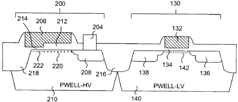
[0036] Figure 7A is a plan view of a single-transistor anti-fuse memory cell,
according
to an embodiment of the present invention. Anti-fuse memory cell 200 is
typically formed in a
memory array, and includes the previously described variable thickness gate
oxide of U.S.
Patent No. 7,402,855. Anti-fuse memory cell 200 includes active area 202,
bitline contact
204, polysilicon gate 206 and diffusion region 208 formed in the active area
202. The bitline
contact 204 makes electrical contact with diffusion region 208. Anti-fuse
memory cell 200 is
formed in a common well 210, which is a high voltage well such as the high
voltage p-type
well that is used for I/O transistors. Common well 210 can be the same as
common well 114
of Figure 6B. Underneath the polysilicon gate 206 and covering the channel
area (not shown)
is a variable thickness gate oxide. The dashed outline 211 defines the areas
in which a thick
gate oxide is to be formed via a thick gate oxide definition mask during the
fabrication
process.
-13-
CA 02646367 2008-12-23
[0037] Figure 7B is a cross-sectional view of anti-fuse memory cell 200 taken
along
line C-C. For comparison purposes, Figure 7B also shows a cross-sectional view
of the same
core circuit transistor 130 shown in Figure 6B, that would be formed in the
same substrate as
anti-fuse memory cell 200. Figure 7B clearly shows the variable thickness gate
oxide
underneath polysilicon gate 206, which has a thick gate oxide portion 212 and
a thin gate
oxide portion 214. The thick gate oxide portion 212 is defined using the thick
gate oxide
definition mask 211. The diffusion region 208 has an LDD region extending
under the
sidewall spacer adjacent polysilicon gate 206, and field oxide such as STI 216
and 218 are
included for isolating anti-fuse memory cell 200 from other memory cells or
core circuits,
such as core circuit transistor 130. Core circuit transistor 130 includes the
same numbered
elements previously described in Figure 6B. Once again, this core circuit
transistor 130 can
be representative of all transistors used in the core circuits for operating
the memory array,
such as control logic or decoding logic for example, and is formed in well 140
that is different
than well 210. In the present example, well 140 is a low voltage p-type well
(PWELL-LV),
which differs from the high voltage p-type well (PWELL-HV), 210.
[0038] Several notable features of the anti-fuse memory cell 200 are now
described.
The thin gate oxide portion 214 of the variable thickness gate oxide and the
thin gate oxide
134 of the core circuit transistor 130 are identical to each other, meaning
that they are
formed with substantially the same thickness. U.S. Patent No. 7,402,855
teaches that the
thin gate oxide portion 214 is first formed at the same time that thin gate
oxides for LV
transistors are formed. Although the gates oxides 214 and 134 are the same,
the threshold
voltage of the anti-fuse device and the core circuit transistor 130 are
different. As previously
discussed, core circuit transistor 130 includes an LV transistor Vt implant
142 in the channel
between the diffusion regions 136 and 138 to raise the Vt from the native Vt
due to well 140.
The channel region between diffusion region 208 and STI 218 is exposed to the
same HV
transistor Vt adjust implant step, thereby resulting in different Vt implants
220 and 222 due to
the differing thicknesses of the variable thickness gate oxide. The channel
region underneath
thick gate oxide portion 212 will have HV transistor Vt implant 220 that is
used for adjusting
the Vt of 1/0 transistors to a desired value, such as 0.6 volts for example.
The channel region
underneath thin gate oxide portion 214 will have Vt implant 222 that results
in a Vt being a
scaled factor of the resulting Vt corresponding to the thick gate oxide
portion 212. Once
again, this scaling factor is related to the difference in thickness between
thick gate oxide
-14-
CA 02646367 2008-12-23
portion 212 and the thin gate oxide portion 214. Alternately, the channel
region under the thin
gate oxide portion 214 can be masked during the HV transistor Vt adjust
implant step,
thereby preventing any Vt adjust implantation into this region. Accordingly,
the Vt under the
thin gate oxide portion 214 will be similar to the native Vt determined by the
well doping of
well 210, but partially modified by the HV transistor Vt implantation due to
mask alignment
error. The threshold voltage of the anti-fuse device will be lower than the
threshold voltage of
the core transistor having substantially the same thin gate oxide thickness.
[0039] An alternate embodiment of a two transistor anti-fuse memory cell is
shown in
Figure 8A. Figure 8A is a plan view of a two-transistor anti-fuse memory cell,
according to an
embodiment of the present invention. Anti-fuse memory cell 300 is typically
formed in a
memory array, and includes an access transistor and an anti-fuse transistor.
The access
transistor can be identical to the one shown in Figure 6A, and includes active
area 302,
bitline contact 304 and polysilicon gate 306. The anti-fuse transistor can
have a variable
thickness gate oxide identical to the one shown in Figure 7A, and includes
active area 302
and polysilicon gate 308. A first diffusion region 310 is formed in the active
area 302 between
polysilicon gates 306 and 308, while a second diffusion region 312 is formed
in the active
area 302 on the other side of the polysilicon gate 306. The bitline contact
304 makes
electrical contact with second diffusion region 312. Both the access
transistor and the anti-
fuse transistor are formed in a common well 314. More specifically, the common
well 314 is a
high voltage well, such as high voltage p-type well that is used for I/O
transistors. The
dashed outline 315 defines the areas in which a thick gate oxide is to be
formed via a thick
gate oxide definition mask during the fabrication process. Underneath the
polysilicon gate
306 and covering the channel area (not shown) is a thick gate oxide.
[0040] Figure 8B is a cross-sectional view of anti-fuse memory cell 300 taken
along
line D-D. For comparison purposes, Figure 8B also shows a cross-sectional view
of the same
core circuit transistor 130 shown in Figure 6B, that would be formed in the
same substrate as
anti-fuse memory cell 300. Figure 8B clearly shows a thick gate oxide 316
underneath
polysilicon gate 306, and the variable thickness gate oxide having a thick
gate oxide portion
318 and a thin gate oxide portion 320 underneath polysilicon gate 308. The
thick gate oxide
316 and the thick gate oxide portion 318 are both defined using the thick gate
oxide definition
mask 315. The diffusion regions 310 and 312 have LDD regions extending under
the
sidewall spacers adjacent polysilicon gates 306 and 308, and field oxide such
as STI 322
-15-
CA 02646367 2008-12-23
and 324 are included for isolating anti-fuse memory cell 300 from other memory
cells or core
circuits, such as core circuit transistor 130. Core circuit transistor 130
includes the same
numbered elements previously described in Figure 6B.
[0041] Several notable features of the anti-fuse memory cell 300 are now
described.
The thin gate oxide portion 320 of the variable thickness gate oxide and the
thin gate oxide
134 of the core circuit transistor 130 are identical to each other, meaning
that they are
formed with substantially the same thickness. Although the gates oxides 320
and 134 are the
same, the threshold voltage of the anti-fuse device and the core circuit
transistor 130 are
different. As previously discussed, core circuit transistor 130 includes an LV
transistor Vt
implant 142 in the channel 140 between the diffusion regions 136 and 138 to
raise the Vt
from the native Vt due to well 140. The channel region between diffusion
region 310 and STI
324 is exposed to the same HV transistor Vt adjust implant step, thereby
resulting in different
Vt implants 326 and 328 due to the differing thicknesses of the variable
thickness gate oxide.
The channel region underneath thick gate oxide portion 318 will have HV
transistor Vt
implant 326 that is used for adjusting the Vt of I/O transistors to a desired
value, such as 0.6
volts for example. The channel region underneath thin gate oxide portion 320
will have a Vt
implant 328 that results in a Vt being a scaled factor of the resulting Vt
corresponding to the
thick gate oxide portion 318. Once again, this scaling factor is related to
the difference in
thickness between thick gate oxide portion 318 and the thin gate oxide portion
320.
Alternately, the channel region under the thin gate oxide portion 320 can be
masked during
the HV transistor Vt adjust implant step, thereby preventing any Vt adjust
implantation into
this region. Accordingly, the Vt under the thin gate oxide portion 320 will be
the native Vt due
to well 210. The thick gate oxide 316 of the access transistor is thicker than
the gate oxide of
any transistor in the core circuits, but has an HV transistor Vt implant 330
substantially the
same as an I/O transistor. Since the gate oxide thicknesses of portions 318
and 316 are
substantially the same, then Vt implants 320 and 336 will be substantially the
same. In the
present embodiment, the channels under thick gate oxide 318 and thin gate
oxide portion
320 are exposed to the same HV transistor Vt implantation step.
[0042] The previously shown anti-fuse memory cells are examples of possible
shapes for the two-transistor and the single transistor anti-fuse memory
cells. Other possible
shapes for the anti-fuse memory cells can be used, as demonstrated in commonly
owned
U.S. Patent Publication No. 2007/0257331. U.S. Patent Publication No.
2007/0257331
-16-
CA 02646367 2008-12-23
teaches anti-fuse memory cell shapes that minimize the thin gate oxide area.
Accordingly,
the embodiments of the present invention can be applied to anti-fuse memory
cells having
the alternate shapes shown in U.S. Patent Publication No. 2007/0257331.
[0043] In all the anti-fuse memory cell embodiments shown in Figures 6B, 7B
and 8B,
all the transistors of the anti-fuse memory cell are formed in the same high
voltage well,
where the high voltage well can be the same as the one used for I/O
transistors. Since the
high voltage well is inherently designed to minimize leakage between adjacent
devices
separated by STI, the Vt implant of the anti-fuse device can be omitted. This
results in a Vt
that is lower than any core circuit transistor on the same semiconductor
substrate.
Alternately, the anti-fuse devices have channels exposed to the same high
voltage Vt implant
step that the thick gate oxide access transistor or thick gate oxide portion
are exposed to.
This results in a Vt for the anti-fuse device that differs from the Vt of any
core circuit
transistor, resulting in better controlled or relatively lower Vt, and/or
lower silicon damage due
to the ion implantation. The fabrication of the anti-fuse memory cells shown
in Figures 6B, 7B
and 8B uses existing CMOS process steps for fabricating the I/O transistors
and the core
circuit transistors without any additional masking steps, thereby minimizing
the fabrication
cost of the entire semiconductor device.
[0044] Figures 9A to 9G shows various steps in a CMOS process used to form the
anti-fuse memory cell of Figure 6B, at the same time a core circuit transistor
is formed. Only
specific steps are shown in Figures 9A to 9G for illustrating the differences
between the anti-
fuse memory cell embodiment of the present invention and a core circuit
transistor. Persons
skilled in the art understand that other non-illustrated steps are executed
for forming the
structures of the transistors. In Figure 9A, the STI oxide 400 have been
formed in the
memory array area 402, core circuit area 404 and the I/O circuit area (not
shown). An implant
mask 406 is formed over the core circuit area 404, and the exposed substrate
not covered by
mask 406 is bombarded with p-type ions for forming a high voltage p-type well.
It is noted
that the high voltage p-type well for the I/O transistor structures are formed
at the same time.
Subsequently, an optional high voltage Vt adjust implant for the memory array
area 402 and
the I/O transistors is performed. It is noted that the high voltage Vt adjust
implant may not be
necessary if the desired Vt level is achieved directly using HV well ion
implantation.
Alternately, the area corresponding to the channel region of the anti-fuse
transistor or device
-17-
CA 02646367 2008-12-23
can be masked after the p-type ions for forming a high voltage p-type well
have been
implanted, such that this region does not receive any high voltage Vt adjust
implant.
[0045] In Figure 9B, the memory array area 402 with the PWELL-HV implant and
high voltage Vt adjust implant 408 is covered by mask 410 so that the exposed
substrate
corresponding to core circuit area 404 not covered by mask 410 is bombarded
with p-type
ions for forming a low voltage p-type well. Subsequently, a low voltage Vt
adjust implant for
the core circuit area 404 is performed, which is shown in Figure 9C as low
voltage Vt adjust
implant 412. The structures shown in Figure 9C result from several process
steps. First a
drive-in step is performed to diffuse implanted p-type ions within the
substrate to form the HV
p-type well 414 and the LV p-type well 416. Second, an intermediate oxide 418
is grown over
the substrate of both the memory array area 402 and the core circuit area 404.
Third, a thick
gate oxide (OD2) definition mask 420 is deposited on the intermediate oxide
418 in selected
regions of the memory array area 402 and the I/O circuit area (not shown) for
defining thick
gate oxides. The absence of mask 420 in the core circuit area means that no
high voltage
transistor is to be formed therein. In a following oxide etching step, any
intermediate oxide
418 not covered by mask 420 is etched down to the substrate surface in
preparation for thin
gate oxide formation.
[0046] In Figure 9D, a thin oxide 422 is formed on the exposed substrate
surface in
the memory array area 402 and the core circuit area 404. There are two
different techniques
which can be used for forming the thin oxide 422. A first technique is the one
shown in Figure
9D, where the thin oxide 422 is thermally grown on the exposed substrate
surface. In this
technique, the thin oxide 422 will also grow underneath the intermediate oxide
418, which
pushes the intermediate oxide 418 up and away from the substrate surface. The
growth rate
underneath the intermediate oxide 418 is lower than in areas where there is no
intermediate
oxide 418 covering the substrate surface. While it is not shown in Figure 9D,
the intermediate
oxide 418 is lifted above the substrate surface by thermally grown thin oxide.
A second
technique is deposition of the thin oxide 422 over the exposed substrate
surface and the
exposed surface of the intermediate oxide 418. In either case, the resulting
thick gate oxide
will be a sum of the intermediate oxide plus thermally grown thin oxide from
underneath the
intermediate layer or thin oxide deposited on top of the intermediate layer.
[0047] Since the I/O transistors are intended to have thick gate oxides, the
I/O
transistor areas would already have the intermediate oxide 418. Following the
growth of the
-18-
CA 02646367 2008-12-23
thin oxide 422, gate polysilicon 424 is deposited over the entire substrate,
which includes the
memory array area 402, the core circuit area 404, and any I/O transistor
areas. As shown in
Figure 9D, the gate polysilicon 424 is deposited over the thin oxide 422 and
the thicker
intermediate oxide 418. In order to define the specific shape of the gate
polysilicon 424, a
gate mask 426 is deposited over selected areas of the gate polysilicon 424.
Following
deposition of the gate mask 426, all the exposed gate polysilicon 424 not
covered by gate
mask 426 is etched away, leaving stacks of polysilicon gates over thin or
thick (intermediate)
oxides in the memory array area 402, the core circuit area 404, and the I/O
circuit area.
[0048] Figure 9E shows three such stacks resulting from the gate polysilicon
etch
step, two being in the memory array area 402 and one being in the core circuit
area 404. In
memory array area 402, the stack consisting of gate polysilicon 424 over thin
oxide 422 is
the anti-fuse transistor device while gate polysilicon 424 over the thick
(intermediate) oxide
418 is the access transistor. In core circuit area 404, the stack consisting
of gate polysilicon
424 over thin oxide 422 is a low voltage transistor used in a logic circuit,
for example. In
Figure 9E, a diffusion mask 428 is deposited over memory array area 402 and
the I/O circuit
area, thereby allowing for the formation of LDD regions (not shown) and
sidewall spacers
430 adjacent to the gate polysilicon 424 of all the low voltage transistors in
the core circuit
area 404. After formation of the sidewall spacers 430, the exposed substrates
are exposed to
n-type diffusion implantation for forming source and drain diffusion regions
for all the low
voltage transistors in the core circuit area 404. The resulting LDD regions
432 and diffusion
regions 434 for the low voltage transistors in the core circuit area 404 are
shown in Figure
9F, and have concentrations specifically designed for the low voltage
transistors.
[0049] In Figure 9F the diffusion mask 428 has been removed, and the low
voltage
transistors in the core circuit area 404 are covered with another diffusion
mask 436. Now the
transistors of the memory array area 402 are exposed to LDD implants, the
formation of
sidewall spacers 438, and diffusion region implantation. Figure 9G shows the
completed anti-
fuse memory cell having LDD regions 440 and diffusion regions 442, and the
completed low
voltage transistor in the core circuit area 404. The resulting LDD regions 440
and diffusion
regions 442 for the high voltage transistors in the memory array area 402 are
shown in
Figure 9F, and have concentrations specifically designed for the high voltage
transistors. At
this point, all the transistors of the device are subjected to n-type implant
diffusion annealing
to activate the implanted dopants and to heal any implant damage. It is noted
that the anti-
-19-
CA 02646367 2009-11-13
fuse memory cell and low voltage transistor of Figure 9F are the same as the
corresponding
ones shown in Figure 6B. Fabrication of the anti-fuse memory cells and all
other transistors
is completed, and subsequent process steps would be executed for forming
bitline contacts
and depositing conductive tracks for interconnecting the transistor devices.
[0049] Figures 9A to 9G illustrate example steps in a CMOS fabrication process
for
forming a two-transistor anti-fuse memory cell and a low voltage core circuit
transistor. The
anti-fuse transistor and the low voltage core circuit transistor have thin
gate oxides formed
using the same gate oxide formation process, but have Vt implants and
effective thresholds
which differ. Because the entire high voltage p-well 414 is initially
subjected to a common
high voltage Vt implant, both the access transistor and the anti-fuse
transistor have the same
implant, but will have different effective Vt's. More specifically, the high
voltage Vt implant is
intended to ensure that the effective Vt of the access transistor having the
thick gate oxide is
at a specific value, such as 0.6V for example. Therefore the effective Vt of
the anti-fuse
transistor is less than 0.6V since its gate oxide is thinner. In an alternate
embodiment, the
channel under the thin oxide 422 of the anti-fuse transistor can be inhibited
from receiving
the high voltage Vt implant, thereby further reducing its effective Vt. The
low voltage core
circuit transistor is subjected to a low voltage Vt implant, which is intended
to ensure that its
effective Vt is at a specific value, such as 0.6V for example. In any case,
the resulting
effective Vt of the anti-fuse transistor will always be different than that of
any low voltage core
circuit transistor.
[0050] Figures 10A to 10G show various steps in a CMOS process used to form
the
anti-fuse memory cell of Figure 7B, at the same time a core circuit transistor
is formed. Only
specific steps are shown in Figures 10A to 10G for illustrating the
differences between the
anti-fuse memory cell embodiment of the present invention and a core circuit
transistor.
Persons skilled in the art understand that other non-illustrated steps are
executed for forming
the structures of the transistors. In Figure 10A, the STI oxide 500 are formed
in the memory
array area 502, core circuit area 504 and the I/O circuit area (not shown). An
implant mask
506 is formed over the core circuit area 504, and the exposed substrate not
covered by mask
506 is bombarded with p-type ions for forming a high voltage p-type well. It
is noted that the
high voltage p-type well for the I/O transistor structures are formed at the
same time.
Subsequently, a high voltage Vt adjust implant for the memory array area 502
and the I/O
transistors is performed. Alternately, the area corresponding to the channel
region of the anti-
-20-
CA 02646367 2008-12-23
fuse device portion can be masked after the p-type ions for forming a high
voltage p-type well
have been implanted, such that this region does not receive any high voltage
Vt adjust
implant.
[0052] In Figure 10B, the memory array area 502 with the high voltage Vt
adjust
implant 508 is covered by mask 510 so that the exposed substrate corresponding
to core
circuit area 504 not covered by mask 510 is bombarded with p-type ions for
forming a low
voltage p-type well. Subsequently, a low voltage Vt adjust implant for the
core circuit area
504 is performed, which is shown in Figure 1 OC as low voltage Vt adjust
implant 512. It
should be noted at this time that there are different variations in the well
formation and Vt
adjust implantation process, of which the above described sequence is one
example
process. For example, the same well implant can be used for both low and high
voltage
transistors, but different Vt adjustment implants can be used. Alternately,
two separate well
implants can be used for the low and high voltage transistors, while the same
Vt adjust
implant is used for both wells. It may even be possible to omit certain Vt
adjust implants.
Maximum flexibility is obtained when both low and high voltage transistors
have their own
well implants and Vt adjust implants. This may be desired to obtain a high
level of control
over the well profiles and precision of the transistor threshold voltages.
There may be
situations where different high voltage transistors are available in a
process, therefore each
different type of high voltage transistor may have different well and Vt
adjust implants. To
improve cost efficiency, a Vt adjust implant can be done using existing masks,
such as a P-
well or diffusion (LDD) masks for example.
[0053] The structures shown in Figure 10C result from several process steps.
First a
drive-in step is performed to diffuse implanted p-type ions within the
substrate to form the
high voltage p-type well 514 and the low voltage p-type well 516. Second, an
intermediate
oxide 518 is grown over the substrate of both the memory array area 502 and
the core circuit
area 504. Third, a thick gate oxide (OD2) definition mask 520 is deposited on
the
intermediate oxide 518 in selected regions of the memory array area 502 and
the I/O circuit
area (not shown) for defining thick gate oxides. The absence of mask 520 in
the core circuit
area means that no high voltage transistor is to be formed therein. In a
following oxide
etching step, any intermediate oxide 518 not covered by mask 520 is etched
down to the
substrate surface in preparation for thin gate oxide formation.
-21 -
CA 02646367 2008-12-23
[0054] In Figure 10D, a thin oxide 522 is grown on the exposed substrate
surface in
the memory array area 502 and the core circuit area 504. Since the I/O
transistors are
intended to have thick gate oxides, the I/O transistor areas would already
have the
intermediate oxide 518. Following the growth of the thin oxide 522, gate
polysilicon 524 is
deposited over the entire substrate, which includes the memory array area 502,
the core
circuit area 504, and any I/O transistor areas. As shown in Figure 10D, the
gate polysilicon
524 is deposited over the thin oxide 522 and the thicker intermediate oxide
518. In order to
define the specific shape of the gate polysilicon 524, a gate mask 526 is
deposited over
selected areas of the gate polysilicon 524. It is noted that the variable
thickness gate oxide of
the single transistor anti-fuse memory cell is now defined by the position of
the gate mask
526 in the core circuit area 504. More specifically, gate mask 526 in the core
circuit area 504
covers both the thin oxide 522 and the thicker intermediate gate oxide 518.
Following
deposition of the gate mask 526, all the exposed gate polysilicon 524 not
covered by gate
mask 526 is etched away, leaving stacks of polysilicon gates over thin and
thick
(intermediate) oxides in the memory array area 502, the core circuit area 504,
and the I/O
circuit area.
[0055] Figure 1 OE shows two such stacks resulting from the gate polysilicon
etch
step, one being in the memory array area 502 and one being in the core circuit
area 504. In
memory array area 502, the stack consisting of gate polysilicon 524 over
variable thickness
oxides 518 and 522 is the anti-fuse transistor device. In core circuit area
504, the stack
consisting of gate polysilicon 524 over thin oxide 522 is a low voltage
transistor used in a
logic circuit, for example. In Figure 10E, a diffusion mask 528 is deposited
over memory
array area 502 and the I/O circuit area, thereby allowing for the formation of
LDD regions (not
shown) and sidewall spacers 530 adjacent to the gate polysilicon 524 of all
the low voltage
transistors in the core circuit area 504. After formation of the sidewall
spacers 530, the
exposed substrates are exposed to n-type diffusion implantation for forming
source and drain
diffusion regions for all the low voltage transistors in the core circuit area
504. The resulting
LDD regions 532 and diffusion regions 534 for the low voltage transistors in
the core circuit
area 504 are shown in Figure 1 OF, and have concentrations specifically
designed for the low
voltage transistors.
[0056] In Figure 1 OF the diffusion mask 528 has been removed, and the low
voltage
transistors in the core circuit area 504 are covered with another diffusion
mask 536. Now the
-22-
CA 02646367 2008-12-23
transistors of the memory array area 502 are exposed to LDD implants, the
formation of
sidewall spacers 538, and diffusion region implantation. Figure 10G shows the
completed
anti-fuse memory cell having LDD region 540 and diffusion region 542, and the
completed
low voltage transistor in the core circuit area 504. The resulting LDD region
540 and diffusion
region 542 for the high voltage transistors in the memory array area 502 are
shown in Figure
10G, and have concentrations specifically designed for the high voltage
transistors. At this
point, all the transistors of the device are subjected to n-type implant
diffusion annealing to
activate the implanted dopants and to heal any implant damage. It is noted
that the anti-fuse
memory cell and low voltage transistor of Figure 10F are the same as the
corresponding
ones shown in Figure 7B. Fabrication of the anti-fuse memory cells and all
other transistors
is completed, and subsequent process steps would be executed for forming
bitline contacts,
and for depositing conductive tracks for interconnecting the transistor
devices.
[0057] Figures 10A to 10G illustrate example steps in a CMOS fabrication
process for
forming a single transistor anti-fuse memory cell having a variable thickness
gate oxide, and
a low voltage core circuit transistor. The anti-fuse device of the single
transistor anti-fuse
memory cell and the low voltage core circuit transistor have thin gate oxides
formed using
the same gate oxide formation process, but have Vt implants and effective
thresholds which
differ. Because the entire high voltage p-well 514 is initially subjected to a
common high
voltage Vt implant, both the access transistor portion and the anti-fuse
device portion of the
single transistor anti-fuse memory cell have the same implant, but will have
different effective
Vt's. More specifically, the high voltage Vt implant is intended to ensure
that the effective Vt
of the access transistor portion having the thick gate oxide is at a specific
value, such as
0.6V for example. Therefore the effective Vt of the anti-fuse device is less
than 0.6V since its
gate oxide is thinner. In an alternate embodiment, the area under the thin
oxide 522 of the
variable thickness gate oxide can be inhibited from receiving the high voltage
Vt implant,
thereby further reducing its effective Vt. The low voltage core circuit
transistor is subjected to
a low voltage Vt implant, which is intended to ensure that its effective Vt is
at a specific value,
such as 0.6V for example. In any case, the resulting effective Vt of the anti-
fuse device will
always be different than that of any low voltage core circuit transistor.
[0058] The fabrication process for forming the anti-fuse memory cells of
Figures 6B
and 7B is summarized in the flow chart of Figure 11. Wells for the anti-fuse
memory cells in
the memory array area and the transistors in the I/O circuit area are formed
in step 600,
-23-
CA 02646367 2008-12-23
which corresponds to the fabrication steps shown in Figures 9A and 10A. A Vt
adjust implant
is introduced into these wells after well ion implantation, where the Vt
adjust implant is
designed for high voltage transistors. In the present example, the wells are
designed for high
voltage transistors. In an alternate embodiment, channel regions under thin
oxide can be
masked so that they do not receive any Vt adjust implant. At step 602, wells
for the core
circuit area are implanted, followed by a Vt adjust implant, which corresponds
to the
fabrication steps shown in Figures 9B and 10B. Thick gate oxide is grown for
the I/O
transistors and the access transistors of the anti-fuse memory cells in the
memory array area
at step 604, which corresponds to the fabrication steps shown in Figures 9C
and 10C. Then
thin gate oxide is grown for the anti-fuse transistor/devices in the memory
array area and the
core circuit transistors at step 606, which corresponds to the fabrication
steps shown in
Figures 9D and 10D. Step 606 can include thermally growing the thin oxide or
deposition of
the thin oxide. In either case, the thick gate oxide grown in step 604 is
increased in thickness
as the formed thin gate oxide is added to the thick gate oxide. Finally at
step 608, the
polysilicon gates for all the transistors are formed and the diffusion regions
for the I/O
transistors, anti-fuse memory cell transistors and the core circuit
transistors are implanted.
This corresponds to the fabrication steps shown in Figures 9D-9F and 10D-10F.
[0059] The previous Figures show one anti-fuse memory cell in isolation from
other
anti-fuse memory cells in a memory array. Figures 12 to 14 are plan view
layout illustrations
of multiple anti-fuse memory cells of the present embodiments arranged in a
memory array.
[0060] Figure 12 is a plan view layout of a two-transistor anti-fuse memory
cell
memory array according to an embodiment of the present invention. Each two-
transistor anti-
fuse memory cell in memory array 700 has both polysilicon gates 106 and 108
connected to
each other, and have the same structure as anti-fuse memory cell 100 of
Figures 6A and 6B.
In order to maintain clarity of the drawing, only polysilicon gates 106 and
108 of one anti-fuse
memory cell are annotated. Memory array 700 is shown to include six anti-fuse
memory
cells, where three are arranged in a first row 702 and another three are
arranged in a second
row 704. A first wordline WLi is connected to the anti-fuse memory cells of
row 702, while a
second wordline WLi+1 is connected to the anti-fuse memory cells of row 704.
The dashed
outline 705 defines the areas in the memory array in which a thick gate oxide
is to be formed
via a thick gate oxide definition mask during the fabrication process. In the
configuration
shown in Figure 12, each pair of memory cells from rows 702 and 704 share a
common
-24-
CA 02646367 2008-12-23
diffusion region 706 and a common bitline contact 708. Each bitline contact is
connected to a
different bitline, such as bitlines BLn, BLn+1 and BLn+2. All the anti-fuse
memory cells are
formed in well 710, which according to the present embodiment is a high
voltage p-type well.
The anti-fuse memory cells of memory array 700 can be formed using the
fabrication steps
shown in Figures 9A-9G.
[0061] Figure 13 is a plan view layout of a two-transistor anti-fuse memory
cell
memory array according to an embodiment of the present invention. Each two-
transistor anti-
fuse memory cell in memory array 800 has individually controlled polysilicon
gates 106 and
108, and have the same structure as anti-fuse memory cell 100 of Figures 6A
and 6B. In
memory array 800, the polysilicon line forming polysilicon gates 106 and 108
of each anti-
fuse memory cell are common to all the anti-fuse memory cells of the row.
Memory array 800
is shown to include six anti-fuse memory cells, where three are arranged in a
first row 802
and another three are arranged in a second row 804. A first wordline WLi is
connected to the
polysilicon gates 106 of row 802 while a first cell plate voltage VCPi is
connected to the
polysilicon gates 108 of row 802. A second wordline WLi+1 is connected to the
polysilicon
gates 106 of row 804 while a second cell plate voltage VCPi+1 is connected to
the polysilicon
gates 108 of row 804. The dashed outline 805 defines the areas in the memory
array in
which a thick gate oxide is to be formed via a thick gate oxide definition
mask during the
fabrication process. In the configuration shown in Figure 13, each pair of
memory cells from
rows 802 and 804 share a common diffusion region 806 and a common bitline
contact 808.
Each bitline contact is connected to a different bitline, such as bitlines
BLn, BLn+1 and
BLn+2. All the anti-fuse memory cells are formed in well 810, which according
to the present
embodiment is a high voltage p-type well. The anti-fuse memory cells of memory
array 800
can be formed using the fabrication steps shown in Figures 9A-9G.
[0062] Figure 14 is a plan view layout of a single transistor anti-fuse memory
cell
memory array according to an embodiment of the present invention. Each single
transistor
anti-fuse memory cell in memory array 900 has one polysilicon gate 206, and
have the same
structure as anti-fuse memory cell 200 of Figures 7A and 7B. In memory array
900, the
polysilicon line forming polysilicon gates 206 of each anti-fuse memory cell
are common to all
the anti-fuse memory cells of the row. Memory array 900 is shown to include
sixteen anti-
fuse memory cells, where four are arranged in each of first row 902, second
row 904, third
row 906 and fourth row 908. Wordlines WLi, WLi+1, WLi+2 and WLi+3 are
connected to the
-25-
CA 02646367 2008-12-23
polysilicon gates 206 of rows 902, 904, 906 and 908 respectively. The dashed
outlines 909
define the areas in the memory array in which a thick gate oxide is to be
formed via a thick
gate oxide definition mask during the fabrication process. In the
configuration shown in
Figure 14, each pair of memory cells from rows 902 and 904 share a common
diffusion
region 910 and a common bitline contact 912. Each bitline contact is connected
to a different
bitline, such as bitlines BLn, BLn+1, BLn+2 and BLn+3. The anti-fuse memory
cells of rows
902 and 904 are formed in a first well 914, while the anti-fuse memory cells
of rows 906 and
908 are formed in a second well 916. Both wells 914 and 916 can be identical
high voltage p-
type wells, but separated from each other via STI oxide formed in the
substrate between
WLi+1 and WLi+2. The anti-fuse memory cells of memory array 900 can be formed
using the
fabrication steps shown in Figures 10A-10G.
[0063] The previously described embodiments can be applied to mask ROM anti-
fuse
devices, such as the ones disclosed in commonly owned PCT Patent Publication
No.
W02008/077240 filed on December 20, 2007. W02008/077240 teaches that an anti-
fuse
memory cell can be programmed by fabricating an electrical connection between
its diffusion
region or channel to a voltage supply.
[0064] The embodiments of the present invention illustrate two-transistor and
single
transistor memory cells having anti-fuse devices with threshold voltages that
differ from low
voltage core circuit transistors. This is achieved by forming the anti-fuse
memory cells in a
well used for high voltage transistors such as I/O transistors, while the core
circuit transistors
are formed in a well typically used for low voltage transistors. Since a
single Vt adjustment
implant and a single LDD implant are applied for both thick gate oxide
transistors and thin
gate oxide transistors in the memory array area, regions of potentially
uncontrolled implant
concentrations and implant damages are eliminated. In contrast, anti-fuse
transistors using
two different wells suffer from the aforementioned disadvantages due to mask
misalignment
causing two or more implant regions to overlap each other. Accordingly, a
higher quality thin
gate oxide for the anti-fuse transistor, or anti-fuse device, results in
lowered effective
threshold and resistance, thereby providing good breakdown characteristics.
[0065] In summary, the thin and thick gate oxide or dielectric regions of the
anti-fuse
memory cell are formed in the same well, or in the wells of the same type and
doping profile.
The core circuit transistors, I/O transistors, or both, use a different well
doping profile than
the wells of the memory array area. The thin and thick gate oxide regions of
the anti-fuse
-26-
CA 02646367 2008-12-23
memory cell can receive the same Vt adjust, or control ion implantation, but
the thin gate
oxide region and the core circuit region receive different Vt control ion
implantation. The
effective Vt of the anti-fuse device will be lower than at least one core
circuit transistor of the
same type and having the same gate oxide thickness.
[0066] The previously presented example embodiments show anti-fuse memory
cells
formed in high voltage p-wells while core circuit transistors are formed in
low voltage p-wells.
Alternately, the anti-fuse memory cells can be formed in high voltage n-wells
while core
circuit transistors are formed in low voltage n-wells.
[0067] In the preceding description, for purposes of explanation, numerous
details
are set forth in order to provide a thorough understanding of the embodiments
of the
invention. However, it will be apparent to one skilled in the art that these
specific details are
not required in order to practice the invention. In other instances, well-
known electrical
structures and circuits are shown in block diagram form in order not to
obscure the invention.
For example, specific details are not provided as to whether the embodiments
of the
invention described herein are implemented as a software routine, hardware
circuit,
firmware, or a combination thereof.
[0068] The above-described embodiments of the invention are intended to be
examples only. Alterations, modifications and variations can be effected to
the particular
embodiments by those of skill in the art without departing from the scope of
the invention,
which is defined solely by the claims appended hereto.
-27-