Note: Descriptions are shown in the official language in which they were submitted.
CA 02646465 2014-01-22
TITLE OF THE INVENTION
APPARATUS FOR MICROARRAY BINDING SENSORS HAVING
BIOLOGICAL PROBE MATERIALS USING CARBON NANOTUBE
TRANSISTORS
BACKGROUND OF THE INVENTION
Field of the Invention
The present invention relates to an apparatus containing microarray binding
sensors having biological probe materials using carbon nanotube transistors
and
various methods for detecting binding of biological target materials thereto.
CA 02646465 2008-09-16
WO 2007/109228 PCT/US2007/006809
Description of the Background
DNA microarrays are powerful tools in molecular biology, and generally
contain an array of hundreds to tens of thousands of genes spotted on a solid
substrate, and which is used to identify and quantify unknown gene samples.
The
microarray technique is predicated upon the property that nucleic acid
hybridization
is highly specific, i.e., cytosine binds only to guanine and thymine to
adenine. Thus,
a specific sequence of nucleic acids, for example, 5' ATCATC3,' will
preferentially
bind with its complementary sequence, 3' TAGTAG5.'
DNA microarrays are invaluable techniques for high throughput monitoring
of gene expression at the transcription level, determining genome wide DNA
copy
number changes, identifying targets of transcription factors, sequencing and,
more
recently, for profiling micro RNA (miRNA) levels in cancer. The central dogma
in
molecular biology is that DNA is transcribed to ribonucleic acid (RNA), and
the
information in the RNA is used to make proteins, by a process called
translation.
Since the function and metabolism of the cell is regulated by the protein
produced in
the cell, many diseases caused by gene mutations, such as cancers, can be
studied by
monitoring the gene expression. Thus, the identification and quantification of
genes
is of particular interest. It is important to know the particular gene or
genes that
contribute to a certain phenotype, and also the amount of the gene that
signifies the
level of the gene expression. There are diseases, however, which are not
necessarily
caused by gene mutation or change in DNA sequence, but which are caused by an
abnormal amount of the gene or abnormal level of gene expression. High
throughput gene identification enables researchers to quickly identify the
genes that
undergo mutations in a certain disease. Comparative gene expression compares
the
level of gene expression, between a cancerous cell and a healthy cell, for
example.
-2-
CA 02646465 2014-01-22
In a typical DNA microarray experiment that relies on fluorescent detection,
comparative gene expression is done by labeling the genes in one cell with one
color
of fluorescent reporter molecules, and genes in the other cell with another.
The
relative intensity of each color is a direct measure of the abundance of the
genes
from the two cells. Given the versatility of DNA rnicroarrays, the impact
thereof on
healthcare is expected to be quite significant if DNA microarrays can be
deployed
widely and inexpensively. It will enable rapid diagnosis of diseases, as well
as
enable drugs to be tailored to each patient to achieve highest effectiveness.
The first reported DNA microarray was fabricated on nylon membranes
using cDNA clones and utilized radioactively labeled targets for detection.
Since
then, many large-scale DNA microarray platforms have been developed, which
have
TM
included, double-stranded cDNA, single stranded short 25mers (Affymetrix ).
mid-
TM
sized Ulmer (Combimatrix ) or long 50-70mers (Nimblegen or Agilent)
oligonucleotides. All of these methods rely upon various combinations of
enzymatic
amplification of the nucleic acid and fluorescent labeling of targets,
hybridization,
and amplification of signal followed by detection by optical scanners.
In a microarray experiment, an array of known single stranded DNA
sequences, called probes, is immobilized on a substrate and later exposed to
an
unknown sei of target genes (or single stranded DNA sequences) that have been
chemically tagged with fluorescent molecules. In places on the array where the
probe and target sequences are complementary, hybridization occurs and the
locations of these specific binding events are reported by the fluorescent
molecules.
A major hurdle of using DNA microarray as a clinical tool is that the
technique is laborious, requires complex protocols, requires large amounts of
reagents, and suffers from low signal to noise ratio and rapid optical
degradation.
3
CA 02646465 2008-09-16
WO 2007/109228 PCT/US2007/006809
While significant strides have been made in fluorescent-based DNA microarray
technology, the methodologies are often time-consuming and in addition rely on
the
determination of fluorescence intensity and the sensitivity is thus limited by
the
ability to detect small numbers of photons. Moreover, fluorescent molecules
suffer
from photobleaching, which means that the fluorescent molecule will stop to
fluoresce after receiving a certain amount of excitation.
A variety of DNA detection schemes has been reported in the literature. The
detection mechanisms involve detection of the existence of the reporter
molecules or
tags, such as radioisotopes, fluorophores, quantum dots, gold nanoparticles,
magnetic nanoparticles, or enzymes, for example. A brief survey of known
fluorescent based DNA microarray, and other label-free electronic field effect
DNA
detection schemes is described below in subsections 1) and 2).
1. Fluorescence-based microarrays
Typically, microarrays are microscope glass slides spotted with thousands of
different genes. The array does not have built-in reader. The detection is
performed
using a fluorescence scanner after hybridization with fluorescent-tagged
target
DNA. There are two ways to make microarrays: (i) spotting cDNA or
oligonucleotides onto the substrate with a robotic spotter, or (ii) direct
oligonucleotide synthesis on the solid support. A robotic spotter uses
thousands of
capillary pins dipped into wells containing different kind of genes and
transports the
genes onto a functionalized solid substrate to create gene spots. Another
approach,
such as the one employed by affymetrix, uses direct oligonucleotide synthesis
on the
substrate. The ingredients are solutions of the four nucleotides: adenine,
guanine,
cytosine and thymine which bear light sensitive protecting group. The process
starts
with a quartz wafer that is coated with a light-sensitive chemical compound
that
-4-
CA 02646465 2008-09-16
WO 2007/109228 PCT/US2007/006809
prevents coupling between the wafer and the first nucleotide of the DNA probe
being created. Lithographic masks are used to either block or transmit light
onto
specific locations of the wafer surface. The exposed spots are now ready to
couple
with a nucleotide. The surface is then flooded with a solution containing
either
adenine, thymine, cytosine, or guanine, and coupling occurs only in those
regions on
the glass that have been deprotected through illumination. The coupled
nucleotide
also bears a light-sensitive protecting group, so the cycle of deprotection
and
coupling until the probes reach their full length, usually 25 nucleotides.
2. Field effect DNA detection
In general, many field effect based biomolecule detection schemes resemble the
structure of ISFET (ion sensitive field effect transistor), which was first
introduced
by Bergveld in 1970. IEEE Transactions on Biomedical Engineering, 17(1): 70-71
(1970). ISFET is similar to the conventional MOSFET (metal oxide semiconductor
field effect transistor), except that the metal layer is replace by an ion-
sensitive
membrane, an electrolyte solution and a counter electrode. EISFET (electrolyte-
insulator-silicon FET) is another acronym that refers to the same structure.
The
drain source current is modulated by field effect from the ions that can reach
the
oxide. ISFET technology has been so well-developed that it has made its way to
the
market as pH meters. Souteyrand et al. is the first to demonstrate label-free-
homo-
oligomer DNA (18-mer and 1000-mer of poly(dA)DNA) hybridization detection
using silicon ISFET. Journal Physical Chemistry B, 101(15): 2980-2985 (1997).
They observed a shift in the flat-band potential of the underlying
semiconductor in
response to the increase of surface charges induced by hybridization between
the
complementary homo-oligomer strands. Several other papers demonstrating
successful field effect DNA detection using silicon ISFET structure are
mentioned
-5-
CA 02646465 2008-09-16
WO 2007/109228 PCT/US2007/006809
below. Pouthas et al. demonstrated field effect detection of 5 pt.M, 10 1.1.M,
20 1.1M of
20-mer oligonucleotide and emphasized the need for low ionic buffer. Physical
Review E, 70(3): 031906 (2004). Fritz et al. were able to detect in real time
as delute
as 2 nM of 12-mer oligonucleotide. Proceedings of the National Academy of
Science USA, 99(22): 14142-14146. They utilized poly L-lyssine (PLL) to
immobilize the probe DNA, and claimed that real time rapid hybridization at
low
ionic buffer (23mM phosphate buffer) was enable by the positively charged PLL
surface that compensated for electrostatic repulsion between complementary DNA
strands. Peckerar et al. demonstrated detection of 1 fM 15-mer DNA. IEEE
Circuits & Davies Magazine 19(2): 17-24 (2003).
Thus, current methods for detecting DNA rely upon various combinations of
enzymatic amplification of nucleic acids and fluorescent labeling of targets,
which
entail enzymatic manipulation of the nucleic acid being tested and chemical
labeling, respectively. These methods are both time consuming and afford
limited
sensitivity.
Further, while more recently, DNA microarray technology has been
deployed as a tool for monitoring gene expression patterns and profiling of
micro
RNA (miRNA) in normal and cancerous tissue, quantification of changes has
typically been optically-based. While this technique is highly sensitive, use
of
optical methods impedes progress in both system miniaturization and in direct
interfacing with data collection electronics.
Hence, a need exists for a method of detecting DNA that overcomes these
disadvantages.
-6-
CA 02646465 2008-09-16
WO 2007/109228 PCT/US2007/006809
SUMMARY OF THE INVENTION
Accordingly, it is an object of the present invention to provide an apparatus
for microarray binding sensors having biological probe materials using carbon
nanotube transistors.
It is a more particular object of the present invention to provide such an
apparatus containing at least one chip, each being positioned on an array of
carbon
nanotube transistors on an insulating substrate and covered by a thin
insulating oxide
or nitride with exposed metallic terminals.
It is, moreover, another object of the present invention to provide a method
of electronically detecting binding of biological probe materials to target
materials
therefor.
It is also an object of the present invention to provide a method for
electronically detecting oligonucleotide - oligonucleotide binding. =
It is further an object of the present invention to provide a method of
forming
iron nanoparticle catalysts for carbon nanotube growth.
Additionally, it is an object of the present invention to provide a process
for
preparing an insulating gate material to afford transistors having improved
conductance.
It is, moreover, an object of the present invention to provide a method of
oligonucleotide immobilization.
Further, it is an object of the present invention to provide a method of
electronically detecting biological materials using bound aptamers.
It is, in addition, an object of the present invention to provide a method of
measuring signal variation as a function of target material concentration, as
well as a
-7-
CA 02646465 2014-01-22
method of electronically determining relative abundances of specific target
materials.
The above objects and others are provided by an apparatus containing:
(a) at least one chip, incorporating an atray of carbon nanotube transistors
on
an insulating substrate and covered by a thin insulating oxide or nitride with
exposed
metallic terminals,
(b) a conducting metal to provide electrical conductivity to the exposed
transistor terminals,
(c) a multiplicity of specific biological probe materials attached on the
=
insulating oxide or nitride layer,
(d) a microfluidic channel above the insulating oxide or nitride layer to
direct
flow of liquid solutions containing biological material;
(e) electronic circuitry configured to detect change in electrical charge due
to
binding of the biological probe materials to target materials in the
biological
material of step d),
(f) means configured to quantitatively correlate detected change in electrical
charge from e) into an amount of bound target material, and
(g) an automated sensing means configured to determine a relative
abundance of specific target materials using the electronic circuitry of e)
and the
means off).
8
CA 02646465 2014-01-22
According to various aspects, the present invention may provide for an
apparatus
comprising: one or more carbon nanotube transistors located on a silicon
substrate, the one or more
carbon nanotube transistors each including a gate electrode, a source
electrode, a drain electrode,
and a carbon nanotube channel bridging the source electrode and the drain
electrode, wherein the
drain electrode and the carbon nanotube channel are covered by a thin
insulating oxide or nitride
layer, wherein the insulating layer insulates the drain electrode and the
carbon nanotube channel
=
from an electrolyte solution, wherein the gate electrode is configured to
contact the electrolyte
solution comprising one or more target biological molecules; one or more
specific probe materials
immobilized on the insulating oxide or nitride later; an electronic circuitry
to detect a change in
electrical charge by each of the one or more carbon nanotube transistors due
to binding of the one or
more specific probe materials with the one or more target biological
molecules; a detector to detect
the change in electrical charge to directly quantify the amount of bound
target biological molecules;
and an automated sensor for determining a relative abundance of the specific
target biological
molecule based on the change in electrical charge.
According to various aspects, the present invention may provide for a method
of
electronically detecting a target biological material in a mixture containing
a target biological
material, wherein the target biological material is selected from the group
consisting of DNA, RNA,
protein, metabolic byproducts, drugs, and whole cells, which method comprises:
a) exposing the
mixture containing the target biological material to the one or more carbon
nanotube transistors of
the apparatus of claim 1; and b) determining an absolute amount of the target
biological material in
the mixture by a change in electrical charge due to binding of the target
biological material to a
probe material on said one or more carbon nanotube transistors.
8a
CA 02646465 2014-01-22
BRIEF DESCRIPTION OF THE DRAWINGS
Figure 1 illustrates the structure of double stranded DNA bonded by hydrogen
bonding.
Electronic detection of DNA, for example, is possible as the phosphate
backbone DNA is charged
when ionized or dissolved in solution.
8b
CA 02646465 2008-09-16
WO 2007/109228 PCT/US2007/006809
Figure 2 is a schematic of a carbon nanotube transistor of the present
invention for liquid gating. The drain source current (I'm) is modulated by
field
effect from the DNA charges adsorbed on the oxide layer.
Figure 3 is a photograph of a carbon nanotube transistor array of the present
invention. Nanotubes bridge the gap between source and drain electrodes. (S)
is the
bonding pad for the common source electrode, and (G) is the bonding pad for
the
gate counter electrode. The square on the other end of (G) is in contact with
the
solution. Unmarked squares are bonding pads for drain electrodes. Shown are 38
transistors in a cell of 3mm x 3mm.
Figure 4 illustrates the geometry for determining line charge next to a
conducting cylinder.
Figure 5 illustrates the geometry for determining capacitance between a
conducting cylinder and a plane.
Figure 6 shows that back gating I-V characteristics improve upon annealing:
(left) before annealing, and (right) after annealing. Annealing temperature
was
500 C for one hour in vacuum.
Figure 7 illustrates a comparison of back-gating and electrolyte-gating on the
same transistor. Triangles of the markers denote the gate voltage sweep
direction
(VDS = -0.1v
Figure 8 illustrates the coupling mechanism of MPTMS to hydroxylated
silicon oxide surface.
Figure 9 illustrates an interface of an electrode in an electrolyte showing
positive surface charges as the electrode and the diffused ions in the outer
Helmholtz
layer (x> 8).
Figure 10 illustrates charge distribution among various interfaces.
-9-
CA 02646465 2008-09-16
WO 2007/109228 PCT/US2007/006809
Figure 11 schematically illustrates DNA adsorbed on the oxide-electrolyte
interface. The length of 15-mer DNA is about 51 A, while the thickness of the
inner
Helmholtz layer is typically about 5 A. An appropriate electrolyte
concentration is
assumed to ensure that the diffuse layer is larger than the DNA.
Figure 12 illustrates the case where the charge to be detected is beyond the
reach of the diffuse layers of the oxide-electrolyte interface.
Figure 13 illustrates transconductance curves of the carbon nanotube
transistor (VDS = -0.1v): (ss) after treated with single-strand DNA;
(unmatched hyb)
incubated with unmatched sequence of DNA; (ds matched) hybridized with
complete matched DNA. Triangles denote sweep direction.
Figure 14 illustrates a feedback circuit to fix IDS by adjusting voltage
applied
to the gate.
Figure 15 is a cross-sectional view of a carbon nanotube transistor. A
semiconducting carbon nanotube is contacted by two electrodes, labeled (S) and
drain (D) on opposite ends, and covered with an insulting oxide barrier. The
source
and drain electrodes have electrical connections (not shown) to bring signals
from
outside of the oxide barrier.
Figure 16 illustrates voltage connections for transconductance
measurements.
Figure 17 a scheme for DNA-DNA hybridization. Functionalized probe
DNAs (pr DNA) are immobilized on the oxide surface using silane-acrydite
binding. A solution containing non-modified target DNA (tar DNA) is introduced
for complementary hybridization.
Figure 18 illustrates a single well transistor setup for a single oligomer
sequence, which contains a redundant set of drain and CNT connections.
-10-
CA 02646465 2008-09-16
WO 2007/109228 PCT/US2007/006809
Figure 19 illustrates an array of transistor wells for implementing
hybridization experiments for multiple target sequences.
Figure 20 illustrates a plot of maximum current versus concentration for a
single transistor sensor. 201.IM probe DNA was used. Monotonic increase of
sensor
current from 100 nM and higher. A nitride-gated transistor was used.
Figure 21 illustrates sensitivity testing whereby sensitivity of the apparatus
is
estimated from the transistor characteristics.
Figure 22 illustrates response with various buffers and treatments. Increase
in conductance is observed as a function of treatment. The largest change in
conductance is due to complementary binding which increased conductance from 2
to 6.5. Subsequent washing and denaturization reduced conductance
significantly.
Figure 23 illustrates characteristics of a transistor fabricated using
aluminum
oxide as a gate material. Significantly improved performance was noted.
Figure 24 show CNTs grown from Fe catalysts prepared by depositing a very
thin layer (less than 1 run) of Fe film by using ultra high vacuum iron
deposition
techniques.
Figure 25 shows CNTs grown out of Fe Pt particles prepared using cluster
fabrication technique.
Figure 26 illustrates an apparatus of the present invention including, by way
of example, a 96 well assay plate.
=
DETAILED DESCRIPTION OF THE PREFERRED EMBODIMENTS
The present invention is predicated, at least in part, upon the provision of a
highly sensitive apparatus based on carbon nanotube transistors for the
electronic
detection of biological probe-target binding. In accordance with the present
-11-
CA 02646465 2008-09-16
WO 2007/109228 PCT/US2007/006809
invention, a single carbon nanotube transistor (CNT) is associated with a
distinct
biological probe material, thereby far surpassing existing technology in
sensitivity,
ease of use and capability of miniaturization. Importantly, the present
apparatus
offers a significant advantage in simplicity of protocol as the method used
therewith
does not require chemical or enzymatic manipulation of the target being
detected.
Further, the present invention does not rely upon optical detection means so
that the present apparatus can be miniaturized. Rather, the present invention
provides, in part, a fabricated nanoplatform using field-effect transistor
(FET)
sensing with a gate terminal of the FET functionalized with an biological
probe
material of interest. While either carbon nanotubes or silicon nanowires may
be
used as FET, carbon nanotubes are preferred.
The present invention, thus, provides an apparatus for biological target
material detection which uses an array of carbon nanotube transistors, with
each
being operated as a field effect transistor. The current versus voltage
characteristics
or transconductance between the source and drain electrodes is measured before
and
=
after a binding event between the biological probe and target materials. By
using a
mathematical relationship, the exact amount of target binding can be
extracted. The
present apparatus employs peripheral electronic networks and amplifiers and
measurement algorithms to perform a highly quantitatively measure of the
amount
of binding of the biological probe-target materials. The data is calibrated
using well
known techniques familiar to artisans in molecular biology. Thus, the present
invention may be used for the same purposes as conventional DNA microarrays
but
with the aforementioned advantages, such as increased sensitivity but without
chemical or enzymatic manipulation of the nucleic acids being detected.
-12-
CA 02646465 2008-09-16
WO 2007/109228 PCT/US2007/006809
The difference in current versus voltage characteristics or transconductance
between the source and drain electrodes before and after a binding, such as an
hybridization event, arises from the known fact that the binding of an
oligonucleotide, for example, such as a target DNA, to a complementary
sequence of
another chain of nucleic acid, termed a probe, in a sequence specific manner
results
in a total charge change on the probe. This may be appreciated from Figure 1,
which shows the occurrences of hydrogen bonds in base pairing (two hydrogen
bonds in an adenine (A) - thymine (T) pair, and three in a cytosine (C)-
guanine (G)
pair), and negative charges carried by the phosphate backbone.
The apparatus of the present invention is advantageous as it can be
miniaturized and the methodologies of using the apparatus exhibit at least
five major
advantages for detecting DNA, which are:
(i) since the apparatus detects charge, the sample does not need a labeling
step, whereby the process is less laborious;
(ii) since the methodology is label-free, the sensitivity is better than the
fluorescent detection scheme, because in fluorescent detection schemes, the
sensitivity depends both on the photodetector and the completeness of the
fluorescent tagging;
(iii) the methodology does not suffer from photobleaching, and the apparatus
can be used for detection many times if time averaging is needed;
(iv) application of electric field can increase the hybridization reaction
rate,
which increases the throughput of the assay; and
(v) the methodology does not use optical detection means, thus facilitating
miniaturization.
-13-
CA 02646465 2008-09-16
WO 2007/109228 PCT/US2007/006809
The method described in detail below allows for the sensitive and specific
detection of nucleic acid hybridization without the need of for extensive
chemical or
enzymatic manipulation of the DNA or RNA. The applications of the present
apparatus and methodologies using the same are extensive. A few may be
mentioned:
1. Monitoring Gene expression: research and for diagnostics and predicting
prognosis
2. Monitoring micro RNA (miRNA) expressions, (MicroRNAs (rniRNAs) are
small, RNA molecules encoded in the genomes of plants and animals. These
highly conserved, -21-mer RNAs regulate the expression of genes by binding
to the anywhere along the mRNA but particularly the 3'-untranslated regions
(3'-UTR) of specific mRNAs. They have been reported to be differentially
expressed in cancers of specific types and there is evidence that certain
profiles may predict the patient outcome in cancer.
3. Detecting DNA copy number changes, performing electronic comparative
genomic hybridization, detecting deletions in chromosomal regions.
4. Sequencing entire genes, may replace the current gel based sequencing
techniques.
5. Single Nucleotide Polymorphism detection.
6. Detecting pathogens in the air, blood and body secretions.
DEFINITIONS
As used herein, the following terms are defined as follows:
APTAMER: an oligonucleotide or peptide that binds a specific target
molecule.
-14-
CA 02646465 2008-09-16
WO 2007/109228 PCT/US2007/006809
These oligonucletide and/or peptides have been engineered
through in vitro selection or equivalently SELEX (systematic
evolution of ligands by exponential enrichment) to bind to
various molecular targets such as small molecules, proteins,
nucleic acids, and even cells, tissues and organisms.
Aptamers often molecule recognition properties that rival
antibodies.
CARBON NANOTUBE: A one-atom thick of graphite (called graphene)
rolled
up into a seamless cylinder with a diameter on the order of a
nanometer (nm). The length-to-diameter ratio may be in
excess of 10,000. Carbon nanotubes (CNT) may be either
single-walled (SWNT) or multi-walled (MWNT).
MICROARRAY: This refers to, in the case of DNA for example, a
collection of
DNA spots attached to a solid surface, such as glass, plastic or
silicon chip. The affixed DNA spots are often referred to as
probes or reporters. Microarrays may be fabricated using a
variety of techniques, such as photolithography using ink-jet
printing.
OLIGONUCLEOTTDE: A nucleotide sequence of either DNA or RNA.
The
length of a base sequence is often denoted by 'mei'. Thus, a
=
fragment of 15 bases called a 15-mer.
-15-
CA 02646465 2008-09-16
WO 2007/109228 PCT/US2007/006809
MICROFLUIDIC CHANNEL: A channel having at least one dimension
of less
than 1 mu. Common fluids used in microfluidic devices and
channels thereof are blood samples, bacterial cell suspension,
and protein or antibody solutions, for example. The volume
of fluids within these channels is on the order of a few
nanoliters (nl).
PROBE (OR PROBE MATERIAL): Any biological Material having the
ability
to bind to a target material. Examples include segments of
DNA, RNA, and oligonucleotides and polynucleotides,
generally; cell receptors or viruses. As most commonly used,
the term refers specifically to segments of single-stranded
DNA or RNA having the ability to bind or hybridize, and
thereby detect, complementary sequences in the presence of
large amount of non-complementary DNA and RNA,
respectively.
TARGET (or TARGET MATERIAL): Any biological material having
the
ability to bind to a probe material by hybridization, for
example.
TERMS IN FIGURES:
In Figure 9:
-16-
CA 02646465 2008-09-16
WO 2007/109228 PCT/US2007/006809
x: horizontal axis of the figure, drawn perpendicularly to the
electrode-electrolyte, indicating distance away from the
interface.
p: the vertical axis of the figure to describe the profile of the
electrical charge density, arising from the immobilized DNA
molecules and rearrangement of ions in the buffer solution
0: the origin of the axes, denotes oxide-electrolyte interface
crs : the surface charge density of the immobilized DNA
molecules to the electrode-electrolyte interface.
5: the closest distance from the electrode-electrolyte interface
a solvated ion can approach.
In Figure 10:
x: horizontal axis of the figure, drawn perpendicular to the
electrode-electrolyte interface, indicating distance away from
the interface;
p: the vertical axis of the figure to describe the profile of the
electrical charge density arising from the immobilized DNA
molecules and rearrangement of ions in the buffer solution
0: origin of the x-axis, denoting oxide-electrolyte interface.
-h is the distance from the oxide-electrolyte interface to the
silicon-oxide interface
h: denotes the thickness of the oxide.
: the surface charge density of the immobilized DNA
molecules to the electrode-electrolyte interface.
-17-
.
CA 02646465 2008-09-16
WO 2007/109228 PCT/US2007/006809
3: the closest distance from the electrode-electrolyte interface
a solvated ion can approach.
: the charge density induced in the carbon nanotube.
cr2 : the surface charge density induced in the gate electrode.
00x : the voltage drop across the oxide.
: the voltage drop across the oxide-electrolyte interface
02: the voltage drop across the electrolyte-gate interface.
Vapi, : the applied voltage to the gate and silicon, required to
maintained a fixed charge density on the carbon nanotube,
such that a fixed electrical current is flowing through the
carbon nanotube.
In Figure 11:
p: the vertical axis of the figure to describe the profile of the
electrical charge density, arising from the immobilized DNA
molecules and rearrangement of ions in the buffer solution
: the linear charge density induced in the carbon nanotube.
pavA : the volume charge density of the immobilized DNA,
shown to span to a finite distance to the electrolyte in the
realistic situation, instead of being collapsed to the interface
and treated as a surface charge density in the simplified
model.
In Figure 12:
p: vertical axis of the figure to describe the profile of the
electrical charge density; pion volume charge density of
negative ions in solution; ps: volume charge density of the
-18-
CA 02646465 2008-09-16
WO 2007/109228 PCT/US2007/006809
positive ions in solution which surrounds and screens as; pi:
linear charge density induced in the carbon nanotube; as;
surface charge density of the immobilized molecule of
interest. The figure demonstrates that the immobilized
molecule must be situated close to the interface, otherwise its
change will be screened by the surrounding ions in the
electrolyte and cannot be detected by the device. Any change
in the charge crs will be screened by the surrounding diffuse
layer and has effect to the transistor.
In Figure 13:
ID:drain current;
VGS: voltage across source and gate;
ss: single stranded 15-base oligomer immobilized on the gate;
ds: double stranded DNA, achieved by exposing ss to its
complementary oligomer and hybridized at room temperature;
unmatched hyb: ss exposed to non-complementary sequence
and hybridized under same condition as in ds
In Figure 14:
V is voltage;
R is resistance;
S is source;
D is drain;
I is current;
V.s is drain source voltage; and
G is gate.
=
-19-
CA 02646465 2008-09-16
WO 2007/109228 PCT/US2007/006809
In Figure 15:
S is source;
D is drain;
G is gate;
0õ is insulating oxide; and
G-0õ is gate oxide.
In Figure 16:
Vds is drain source voltage; and
Vg, is gate source voltage.
THE APPARATUS OF THE PRESENT INVENTION
A. Overview of the present apparatus
Semiconducting carbon nanotubes function as channels in between two
conductors and respond to a gating field by modulating the channel
conductance.
Carbon nanotubes are very sensitive charge detectors, and thus are conducive
to
achieving high sensitivity DNA detection, for example. The fabrication of a
carbon
nanotube transistor is easy, simple and well-adaptable to a flexible
substrate. The
cylindrical geometry of the nanotube allows for a less stringent requirement
on gate
oxide thickness. In accordance with the present invention, the nanotube is
insulated
with silicon oxide or nitride, for example, and probe material is immobilized
on the
insulating layer to avoid direct modification of the nanotube by the probe
material or
the electrolyte buffer.
In accordance with another aspect of the present invention, iron nanoparticles
are used as a catalyst for effecting carbon nanotube growth. In particular,
sub-
-20-
CA 02646465 2008-09-16
WO 2007/109228 PCT/US2007/006809
monolayer thin iron films are deposited by thermal evaporation under less than
10-10
atm pressure. Upon exposure to ambient atmospheric pressure, nanoparticles of
iron
oxide are formed, and later reduced by high temperature exposure to hydrogen
during carbon nanotube growth.
B. Carbon nanotube transistors
The present apparatus contains an array containing up to hundreds of
thousands of carbon nanotube transistors, wire-bonded to a circuit board that
is
easily fitted to a platform that houses circuitry of switches that control the
addressing signal to each transistor. Each transistor is spotted with distinct
biological probe material, such as DNA, RNA, peptide or cell surface receptor
domain, so the device mimics a microarray of such probe material, with an
important exception, being among things, that the transistor reader is built
in. For
example, since the DNA backbone is negatively charged only if it is dissolved,
the
charge detection measurement is done with the device in contact with the DNA
electrolyte solution. Thus, the device is well-insulated and encapsulated in a
robust
package to prevent shorting among the leads by the electrolyte solution.
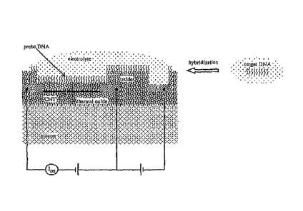
A schematic of a simple apparatus of the present invention is illustrated in
Fig. 2 using DNA as a probe material. The drain (D), source (S) electrodes and
the
carbon nanotube channel bridging the two are insulated from the electrolyte
solution
by an oxide layer. Only the gate (G) electrode is in contact with the
electrolyte
solution. Probe DNA has been immobilized onto the oxide layer on top of the
carbon nanotube channel. The apparatus does not need to be wet all the time.
Only
when charge measurement is performed does the DNA need to be dissolved. The
channel conductance is a function of the field generated by the DNA charge
adsorbed. As a prepared carbon nanotube usually exhibits p-type conduction,
and
-21-
CA 02646465 2008-09-16
WO 2007/109228 PCT/US2007/006809
=
DNA carries negative charges, the channel conductance increases upon
hybridization which causes an increase in the number of charges adsorbed. If
the
drain-source potential is fixed, an increase in channel conductance is
manifested as a
drain-source current (IDs) increase.
The present apparatus or device operates in a feedback mode to fix IDs by
adjusting the gate-source potential (VGs) upon hybridization. In this manner,
the
transistor action mechanism is decoupled from the electrostatics of the
surface
charge adsorption. The VGs shift reduces to a simple capacitance problem and
is
proportional to the change of number of charge adsorbed. Thus, the abundance
of
target DNA, for example, can be quantified by looking at the VGs shift which
indicates the number of hybridization events. When it is desired to identify
DNA,
for example, the present apparatus can achieve the two functionalities of DNA
microarray: (i) gene identification, by looking at which transistor in the
array show
channel conductance increase; and (ii) quantification, by looking at the
amount of
VGs shift.
=
C. Assembling the present apparatus
Carbon nanotubes (CNT) are grown on an insulating oxide substrate, such
as a silicon oxide substrate using chemical vapor deposition (C'VD).
Generally, the
substrate has several hundred nanometers (urn) thickness of thermal oxide on a
p-
type silicon substrate. Catalyst particles, such as iron particles, are
deposited on the
substrate either by iron nitrate dripping or brief evaporation of iron to
generate iron
dusting on the substrate. The growth is effected in a furnace at a temperature
in
excess of about 750 C, preferably about 900 C, with appropriate flow of
methane,
ethylene, hydrogen and argon gas. Carbon nanotubes grew out of the catalyst
and
form a mat on the substrate.
-22-
CA 02646465 2008-09-16
WO 2007/109228 PCT/US2007/006809
From the prepared CNT mat on the silicon dioxide or nitride substrate, the
next step is to connect the nanotube channel to source and drain electrodes,
by
depositing gold film. The substrate is first spin-coated with photoresist,
which is
then patterned using contact photolithography. A chromium adhesion layer and
gold
layer are then deposited on the substrate by thermal evaporation; followed by
lift-off
to remove the gold layer on top of the photoresist. A typical source and drain
separation or the channel length is about 51.tm. Unwanted nanotubes are etched
out
under oxygen plasma.
Figure 3 illustrates a transistor array of 38 transistors in one cell, and all
have
a common source for economizing space. Each electrode (drain or source) is
connected to contact pad for wire bonding. In this case, the contact pad is
200 x 200
tim. The device is intended for liquid gating operation since the DNA should
be
dissolved in the buffer solution so there is also a common gate counter
electrode for
applying gate voltage.
To provide isolation to the nanotubes from the electrolyte buffer, a thin
silicon oxide layer is evaporated on the device, followed by the thick plasma
enhanced CVD (PECVD) of oxide layer (up to ¨ 0.5 gm). The reasons for this
redundancy is that the plasma process destroys the nanotube mat. The oxide
layer at
the active area is RIE (reactive ion etched) back again to get a thickness of
100
nm, while leaving thick oxide on the other part.
Further, the present invention also provides a design and process for forming
insulating gate material. The process entails depositing aluminum gate oxide
by
atomic vapor deposition. A thin layer of less than about 10 nm of silicon
nitride is
deposited on the top layer to improve the protection of the underlying carbon
-23-
CA 02646465 2008-09-16
WO 2007/109228 PCT/US2007/006809
nanotubes from water. The resulting transistors have significantly improved
conductance curves, i.e., less hysterisis, and better uniformity.
1. Design parameters
(a) Oxide thickness
There are two contradicting requirements for the gate oxide thickness. On
the one hand, a thick oxide is desired to minimize electrolyte current
leakage, but on
the other hand, a thin oxide is desired to maximize the gate coupling. The
geometry
of CNT reduces the requirement for extremely thin oxides. A nanotube buried
under
an oxide layer with surface charges on top of the oxide layer may be modeled
by
considering the capacitance between an infinitely long conducting cylinder and
an
infinite plane. Thus, can determine the appropriate oxide layer thickness by
considering a standard textbook problem of an infinite cylinder and a grounded
plane.
The problem of the capacitance between an infinitely long conducting
cylinder and an infinite plane is solved by the method of image. This is an
extension
of the problem of an infinitely long line charge pi (C/m) located at a
distance d from
the axis of a parallel conducting cylinder of radius a. One locates an image
line
charge (p0 that makes the cylinder surface an equipotential surface, and the
dimensions in the problem is shown in Figure 4.
Assigning pi = cif= a2 d makes the cylinder surface equipotential. To solve
for the capacitance between a conducting cylinder and a plane, another
cylinder is
added as shown in Figure 5. The original line change and the image line charge
creates equipotential cylinders around each line charge, with the axes of the
cylinders displaced by di from the respective line charge. If the plane is
inserted
-24-
CA 02646465 2008-09-16
WO 2007/109228 PCT/US2007/006809
right at the center between the two line charges, it will be an equipotential
plane,
since each point on the plane is equidistant from both line charges.
The potential difference between the cylinder surface (M) and the plane (P)
can be written as:
al a
=
2ark- d
=
so that the capacitance per unit iongrit is:
C __________________ = 2Ir6
Vp VA, WC! t a)
But d d ==211¨ a2 M., or ei 14 -1;12 ¨ a ZI
- 2.rre
ta(lita irr2 a2 I a)'
we nolo that .144-42 ¨ tx)sh-1 .r, so we can trj se capaciLattoc as:
207.6_
C" ___________________
=
cost-C:1{:h .0 a ) (1
)
This simple model suggests that the capacitance is a slow function of the
oxide thickness (h), therefore, the requirement of fabricating very thin gate
oxide to
provide optimal gate coupling is largely alleviated. Thus, thick gate oxide
may be
used to avoid electrolyte current leakage without drastic losses in gate
coupling.
Typically, about 50 to 200 urn, preferably about 100 nm thick of oxide, is
used on
top of the drain source gap in between which carbon nanotube channels are
bridging,
and about 250-750 urn, and preferably about 500 run, thick of oxide everywhere
else.
(b) Contact resistance
While the carbon nanotube transistor mechanism of action remains under
investigation, there are rationales and evidence therefor found in the
literature
suggesting IDS is controlled by the gate voltage through: (i) charges induced
in the
nanotube; (ii) modulation of Schottky barrier contact between the
semiconducting
nanotube and the metallic source and drain electrodes; or (iii) combination of
both
(i) and (ii). Unlike conventional MOSFET (metal-oxide-semiconductor field-
effect
-25-
CA 02646465 2008-09-16
WO 2007/109228 PCT/US2007/006809
transistor) where the source and drain are highly doped silicon, the material
of drain
source electrodes for the carbon nanotube transistor used in the present
invention is
gold, a different material from the nanotube channel. Contact resistances
between
drain and channel junction and between channel and source junction are
therefore
inevitable. In practice, regardless of the physical mechanism behind the
transistor
action, the preferred practice is to improve the performance by annealing.
Fig. 6
shows improvement of contact resistance upon vacuum annealing of the device.
The
current level is higher for the same drain-source voltage and the curve shows
less
garble after annealing.
2. Device 1-V curve
As depicted in Fig. 2, the apparatus in operation has to be in contact with
the
electrolyte solution. Gating is done through the electrolyte which is in
contact with
the gate electrode where VGs is applied. This is called electrolyte gating.
However,
there is also another way of gating, which we call back gating, i.e. through
the back
of the body of the silicon which is insulated from the nanotube channel by 300
nm
thick of thermal oxide. Figure 7 shows comparison between back-gating and
electrolyte-gating to the same transistor. It is clear that electrolyte-gating
requires
less voltage range to sweep the transistor on and off, and the hysteresis
effect is less
prominent in the electrolyte-gating. The hysteresis is undesired but
unavoidable and
caused by trapped charges in the oxide layer that move around with the applied
gate
voltage. In practice, the apparatus is should initially biased towards one end
to
always choose the same hysteresis branch with sweeping in only one direction.
-26-
CA 02646465 2008-09-16
WO 2007/109228 PCT/US2007/006809
D. Probe Material immobilization and hybridization
1. immobilization
Probe material is immobilized on the insulating oxide or nitride surface
through silane functionalization. The insulting oxide or nitride surface is
exposed to
brief oxygen plasma to generate hydroxyl groups on the surface, on which (3-
.
mereaptopropyl)trimethoxysilane (MPTMS) can polymerize. The coupling of
MPTMS to hydroxylated silicon oxide surface is shown in Figure 8. Making
aqueous solution of MPTMS substitutes the methoxy groups to hydroxyl groups. A
water molecule is released during the coupling reaction, so it is important to
perform
the coupling in dry environment. But the polymerization of silane molecule
with
other silane molecules is inevitable, leading to formation of large globule of
polymers that induce roughness and heterogeneity on the surface. After the
surface
is functionalized with mercaptan groups, the acrydite-modified probe
oligonucleotides, for example, react readily with the mercaptan groups of the
silane
to form covalent bonds by overnight incubation of the probe oligonucleotides.
We
have used 15-mer oligonucleotide, for example_ The surface is then treated
with 100
mM of sodium acrylate for 15 minutes to passivate unbound MPTMS.
2. Hybridization
Hybridization with unlabeled or untagged target oligonucleotide is done
under normal hybridization condition, i.e. 10 mM phosphate buffer solution
pH7,
0.3 M NaCI. Salt is very important to reduce electrostatic repulsion among two
complementary strands to achieve hybridization. But, high salt or ionic
concentration limits the apparatus sensitivity. Hence, repeated washing steps
are
necessary to reduce the salt without causing dehybridization. Washing is done
at
least three times with gradual decrease of salt concentration 0.3M, 0.1M,
10mM, and
-27-
CA 02646465 2008-09-16
WO 2007/109228 PCT/US2007/006809
finally the device is washed with 0.3M ammonium acetate pH7, which is know to
eliminate salt effectively. Electrolyte gating measurements are taken before
and
after hybridization and are always done under 1mM phosphate buffer pH7.
It has been suggested that target-DNA hybridization onto preimmobilizied
probe-DNA on solid substrate follows the Langmuir adsorption model, which
predicts that at high bulk concentration of the adsorbate, the surface will be
fully
covered by the adsorbate:
,fIC
Where I' is the DNA surface coverage, "max is the maximum DNA surface
coverage, C is the concentration of DNA in the bulk electrolyte, and 11 is
usually
extracted from experiment and is typically in the range of 107 M1 from
fluorescence
or surface plasmon resonance experiment.
E. Electrical Measurements
1. Device Electrostatic Model
(a) Electrolyte capacitance (Gudy-Chapman-Stern model)
When an electrode carrying surface charges is immersed in an electrolyte
solution, ionic space charges of opposite sign will build up in the
electrolyte
solution. Ions in the space charge cannot approach the electrode closer than
the
inner Helmholtz layer, thus they are called out Helmholtz layer or diffuse
layer.
Only chemically specific adsorbed molecules or ions can reside in the inner
Helmholtz layer.
Ions can move around in the electrolyte. The flux of ions consists of
diffusion of ions due to concentration gradient and drift of ions due to an
electric
field. One can imagine that ionic space charges build up close to the charged
electrode, and decay with distance away from the electrode. In the case of
thermal
-28-
CA 02646465 2008-09-16
WO 2007/109228 PCT/US2007/006809
equilibrium where there is no net flux of ions in the solution, a potential
difference is
setup to semiconductor p-n junction.
Using the flux equation j = DVc = qcp.(-6a)=0, and Poisson equation 52 0 /
ax2 --p / a, one can write down several important results in one dimensional
case
for 1:1 electrolyte (e.g. sodium chloride, which ionizes into the same amount
of Na+
and CI in the solution).
The relationship between the electric field and the potential at any arbitrary
position in the electrolyte is:
" fèt &Jai
T
where the potential is set to zero .x .to ,
The above, equation. can be inter:pled to give:
2k. ,Tin (e(x)r 4 kT kTc1Y2
1113th( qtb
where the potential is set at x co.
The above equation can be integrated to give:
2,tc T (thnh(e i(x)itik. 48k
4,
tapi)(0014k.417'
where oois the potential at x=0.
For small argument of hyperbolic tangent, it can be approximated as tanh(x)'---
- x.
We
Let aTethenMqb 0*-A2). Since 00 is the potential at x =0, and
the
potential at x = CO is taken to be zero, than o is the potential drop across
the
electrolyte.
According to the Stern model, ions cannot go arbitrarily close to the
electrode. The ions have a finite size, they are probably solvated, or a layer
of
solvent might separate the ions from the electrode surface. Imagine that the
ions can
only go as close as to the electrode surface. In order to determine the
relation of
-29-
CA 02646465 2008-09-16
WO 2007/109228 PCT/US2007/006809
the potential drop across the electrolyte and the surface charge on the
electrode
surface, from Gauss' law, we can write:
ai$
a,. ¨ tag 0)
ar
And since there is no cluirp.in4betweenx.... (land x 8; then
=
(N "(1 '4*(8)-
-
The4),
(ILL ¨1/111 Th = 11(tIM
_ _iptd_rc sinni c - 0 4)
e 247
Arld finally, the FlOttnaill dil3p tte40313 Olt t Wm) I re is
(2.)
The voltage drop derived in this section is based on thermal equilibrium
assumption, which is attainable when good insulation between the nanotubes and
the
electrolyte exists. Leakage current is ignored in this analysis, however
electrolyte
leakage current is undesirable, because it means that the electrodes have
degraded by
Faraday process.
An applied voltage between the source and the gate counter electrode is the
sum of potential drop across the nanotube channel, the oxide layer, the oxide-
electrolyte interface, and the electrolyte-gate counter electrode interface,
or V app =
Otransislor 00x 01 + 02. Thermal equilibrium is assumed where there is no
net ionic
flux in the electrolyte. The change of the potential drop across the nanotube
channel
can be estimated.
The voltage drop between the electrolyte and the gate counter electrode from
Guoy-Chapman-Stem model derived in the preceding section is given by:
2k T s
,jak 131W , =9
where now cs2 is the surface charge density on the counter electrode. This
potential drop is expected to be about the same before and after DNA
hybridization,
-30-
CA 02646465 2008-09-16
WO 2007/109228 PCT/US2007/006809
=
for example, because the surface charge density depends on the conditions of
the
electrolyte and the counter electrode, which are not changed upon
hybridization.
Now looking at the inner Helmholtz layer, to which probe DNA is attached,
for example, Gauss' law is applied at the interface:
.r,24(=-,E,x)+1=õ,4-{x=5.9=0..õ.
where as is the surface charge density of the immobilized DNA, which will
increase and at most double upon hybridization, ö is in the order of several
Angstrom and denotes the boundary of inner and outer Helmholtz layers.
The voltage drop across the oxide and electrolyte interface is then:
=
2kDr
=-- err=--u-'.03;') F.:(x =45') = 5
8kirc
sinhA lr
" e (Ski;Tecil, z 44
We can eariMate- E. by the electelo fled to the point in Fig. 5: .
'Erõ. 2/71 __ d. -a2. 4112- a2
2.for,õ (ft - d {.4 ).,) =
The vollage drop acros: the Aids: I uyer is ivert by: it, PI "s11-1(111 ).
2n;,,
\knexpoesriuoyõ! E 24.a; MI.,
C0.511-1(7//4h¨a2t(h o-Vh'
Summing op di rho %=vitoge drop terms:
VAN, '132r.zolv., `I' Oar 4' 951 (3)
(b) Voltage shift as a function of adsorbed charge
It is assumed that the apparatus is operating in a feedback mode to keep IDS
constant, so that electrostatics of the adsorbed charges can be decoupled from
the
carbon nanotube transistor action mechanism.
By fixing IDS, is fixed; therefore otransislor and ox are also fixed. The
feedback circuit only needs to compensate for the change of cal due to
hybridization.
Plugging in typical numbers: h 100 nm, a = 2 nm, co, = 3.9 cO, eh/ = 80 so T
300
K, and = 5 A, we can write:
-31-.
CA 02646465 2008-09-16
WO 2007/109228 PCT/US2007/006809
0.051s &Ai -/ 611111321+1-5;c11)-4 0-1'10
G.12,,,f4rnowimr1 i (4)
4.13;7(ers kouihnzi-6,1.5 x10-40. [von))
Typically all voltages involved are in the order of one or two volts. If the
ionic strength of the electrolyte is c = / mM, then the denominator inside the
bracket
of sinh- is 3.79x10⁻³, so the first term is the dominant term.
Probe material, such as DNA, cannot reside completely within the inner
Helmholtz layer. Typically the inner Helmholtz layer is in the order of 5 = 5
A
thick, but the length of 15-mer DNA is 51 A. The more realistic picture of the
interface should look more like the one in Figure 11. The free ion
concentration is
Boltzmann-distributed in energy. We can write down the Poisson's equation as:
= _ __ qichz3)exti q,OW)
= 4r r k, TJ a
or( 1 ¨et- expM 71,00,y4 sinhte4-14.1Ptty4
ay.'. =v 1. kir e kar e ar fc DT a
Unfortunately, the above equation cannot be solved for a closed form
expression. Typically two extreme cases are solved in the textbook: (i) quasi-
neutrality approximation, and (ii) depletion approximation.
In quasi-neutrality approximation, a2 0 / ar2 is assumed to be very small, or
the charge is nearly neutral. The positive ions compensate for the negative
DNA
charges:
coxg-Onfir)::.-Ipact41
¾,k? kar e -int1P0fin114 (5.)
Or
0"1411P91441)
In the other extreme approximation, the depletion approximation, where the
free ions are depleted and cannot compensate for the DNA charges, we can
write:
a)?
2.t...11211--1-44.c0n4t8un,
c
-32-
CA 02646465 2008-09-16
WO 2007/109228 PCT/US2007/006809
(e) Device sensitivity
Simple calculations can be performed to project the minimum concentration
of the 15-mer target DNA needed to induce appreciable voltage shift. Let us
assume we can detect a change of 51 mV, which is the prefactor of the sinh-1
term.
It is a safe assumption indeed, because 51 mV is 2k8T/e. The denominator
inside
the sinlf1 bracket is 3.79x10⁻³, for c = 1mM. If the change is as is equal to
3.79x10-
3, then the 00_, term can be neglected, and the 0/ change is approximately 51
mV.
To achieve 51 mV in the 01 change, we need a surface coverage change of
3.79x1e coul/m2. For 15-mer oligonucleotide, we assume that each base carries
one electron charge in solution, so each molecule carries 15x1.6x10-19 coul.
The
surface coverage needed is then 1.57x10¹⁵ molecule/m2. This surface
concentration
imposes the requirement for the minimum surface density of probe-DNA
immobilization. That is, if the probe DNA is not dense enough, the change in
surface charge upon hybridization to target DNA cannot yield the desired
voltage
change. The maximum DNA surface coverage is achieved when all of the DNA
strands fill up the surface in upright strand orientation. Assuming the strand
radius
is 6A gives:
rnc.= (rrr =Ma with:cute/70:
Using the Langmuir adsorption model, and )6' value of 107M-1, we obtain that
the target concentration in the bulk needed to achieve the desired voltage
change is
Although the sensitivity predicted by the model is only in the order of 20
aM, but it has been shown experimentally that sensitivity down to IM is
achievable
with field effect detection. This suggests that the assumption offl may
actually
-33-
CA 02646465 2008-09-16
WO 2007/109228 PCT/US2007/006809
underestimate the sensitivity. We project that our approach can also achieve
IM
sensitivity.
But the electric field
jP/Avii x_
=
The potential drop across the length (/) of the DNA, is
A,-cotx)n i"n=A112124 t6)
O
95.cipa4i
The quasi neutrality approximation predicts that the potential drop is
proportional to the logarithm of the DNA charges, while the depletion
approximation predicts that the potential drop is linearly proportional to the
DNA
charges. The realistic case may lie in between the two approximations. This is
actually consistent with the behavior of the sink.' function previously
derived from
the potential drop, because sinIci(x) zx for small x, and sinlil(x)::--In(2x)
for large x.
Figure 12 illustrates a situation where the charge to be detected is beyond
reach of the diffuse layer of the oxide-electrolyte interface. Any change in
the
charge as will be screened by the surrounding diffuse layer and has no effect
on the
transistor.
Low ionic salt concentration is used in the electrolyte solution during the
measurement, to ensure that the field from the charge to be detected can reach
the
carbon nanotube channel. Consider in Figure 12, where the charge to be
detected is
farther than the Debye length. The increase in as has no effect on the
transistor
because it only modulates the diffuse layer around it, and the transistor does
not feel
any electric field from as since the field has been screened by the diffuse
layer. So it
-34-
CA 02646465 2008-09-16
WO 2007/109228 PCT/US2007/006809
is very important that the diffuse layer of the oxide-electrolyte interface
overlaps
with the charged biomolecules. The requirement that K has to be large imparts
limitation to the ionic strength (c) of the electrolyte, since is
inversely proport =õite.sikiir,i2,. pt of c. If we take for example a 15-
mer
oligonucleotide and the length of one monomer is 3.4A, then k > 51A, or c <
3.6 in
M.
e-vik.nrene
2. Change of I-V curve upon hybridization: Preliminary proof of
principle
Figure 13 shows the transconductance curve of single strand DNA,
unmatched hybridization, and double strand DNA after completely matched
hybridization. As prepared, carbon nanotube transistors generally show p-type
conduction. Negative charges from DNA adsorbed on the gate serve as extra
negative bias voltage applied that would increase the conductance of nanotube
channel. It is clear that the current level was boosted after the matched
hybridization
due to the increase number of charged adsorbed. A slight increase in current
is still
observed after unmatched hybridization due to non-specific binding. All of the
three
transconductance curves were measured from the same transistor and taken
sequentially from single strand (ss): 5'/AcryditellSpacer18/ATC CTT ATC AAT
ATT -3', hybridization with unmatched sequence: 5'/ATC CTT ATC AAT ATT -3'
(unmatched hyb), and hybridization with matched sequence: 5'/AAT ATT GAT
AAG GAT -3' (ds matched).
Figure 13 illustrates transconductance curves of the carbon nanotube
transistor (VDS=-0.1V) : (ss) after treated with single-strand DNA; (unmatched
hyb)
-35-
CA 02646465 2008-09-16
WO 2007/109228 PCT/US2007/006809
incubated with unmatched sequence of DNA; (ds matched) hybridized with
complete matched DNA.
Triangles denote sweep direction.
F. Summary of the Technique for Microarray Application
The aforementioned discussion relates the expected change in the gate
voltage as a function of the amount of charge deposited on the gate. From a
device
perspective, one can approximate the behavior of the CNT transistor as a PMOS
operating under the so-called triode region. Under this assumption, the drain
current
is modeled as:
111(vv, v,)vd, -;v4,7):1.
(7)
where K is a parameter that determines the sensitivity, vt is the effective
threshold voltage, vds is the applied potential between drain and source, and
vgs is
the applied potential between the gate and source. K and vt are intrinsic
properties
specific to each transistor and may vary from transistor to transistor. In the
presence
of hybridization, the net effect is the change in the threshold voltage vt
which will be
compensated by a corresponding change in vg,
=ay Aro =2K.v,5v,,
e, Dv,
If we employ a feedback circuit such that the current is kept constant, then
we can (7) to zero to obtain. In other words, the change in vas is equal to,
eiv,z tit eis, (9)
This relationship is independent of the transistor property. Furthermore, the
change in vgs can be used as a direct measure of the charge of the bound DNA
molecules given by equations (5) and (6) for quasineutral or depletion
approximations respectively. Thus, the measurement of the change in gate
voltage
-36-
CA 02646465 2008-09-16
WO 2007/109228 PCT/US2007/006809
after hybridization can provide a means to directly quantify the amount of
bound
charge. This approach is a fundamental enabler for gene expression experiments
without the need for labeling.
The general methodology for microarray use as follows. A chip containing
an array of carbon nanotube transistors is fabricated on a suitable substrate.
The
drain, source and gate electrodes are exposed for electrical contact, and an
external
multiplexing circuit is developed for each transistor. A microfluidic channel
made
of PDMS or suitable polymer is fabricated on the chip surface to direct the
flow of
probe and target oligonucleotide, such as DNA, solutions. Prior to DNA
exposure, a
preliminary scan of the transconductance curves will be measured for each
transistor
and will serve to identify working transistors as well as establish the
baseline
characteristics. Next, specific DNA solutions with complementary sequences to
the
target genes and with appropriate terminal modification for substrate binding
are
immobilized on the transistors. An automated spotter immobilizes different
oligonucleotide sequences throughout the array in complete analogy with
existing
fluorescent-based microarrays. Hybridization is then performed on a target
solution,
and the voltage shift at constant current will be measured for each transistor
using
appropriate protocols. The operating point of the current is set at the
steepest point
of the transconductance curve to simultaneously increase the sensitivity and
decrease the data acquisition time. In order to implement the equivalent of
competitive gene expression experiments a second chip is fabricated and the
same
complementary DNA solutions, for example, are immobilized on the second chip.
Hybridization and measurements of the voltage shifts are conducted as in the
previous case, except that the target solution is prepared using the second
sample.
-37-
CA 02646465 2008-09-16
WO 2007/109228 PCT/US2007/006809
The concentration normalization chips corresponding to DNA sequences that are
known to be conserved in both samples.
G. Testing Sensitivity of the Apparatus from Transistor Characteristics
Referring to Figure 21, the following procedure is used to test the
sensitivity
of the present apparatus from transistor characteristics.
Transconductance slope = 1.93 1.1.A/V
Capacitance = 59 if, area = 132 p.m2
To induce IV of VGS change we need a surface charge density of:
1 V x 59(14 5 bas.esx 1.6 x 10'1' Cold
)= 18,6x 1V molecules/we
1 32x 1 Voml
Using Langmuir adsorption model to relate surface density to volume density:
:r KC
r K C
!Wm A
1 5
rmax (maximum surface coverage) is obtained by assuming the DNA to be a
rod like structure with a base of 6 A radius and a height of 3.4 A per base.
Then rma, = 9 x 10¹³ molecules/cm2, if all DNA stand upright, or rmax 3 X 10¹³
molecules/cm2 if all 15-mer DNA lie down horizontally. Typical K4 is 6 x 10⁷
M.
Assuming worst case scenario, that all DNA lie down, we use rmax %--`. 3 x
1013 molecules/cm2. The needed volume concentration to achieve r=3 x 18_6x109
molecules/cm2 in order to induce 3 V change or 3x1.93 j.tA increase in drain
source
current is: =31 pM.
IT. Various Uses of the Present Apparatus
The present apparatus may be used in a large variety of fields and to
accomplish diverse objectives. For example, the apparatus may be used as a
point-
of-care clinical tool to examine certain forms of cancer wherein the knowledge
of
-38-
CA 02646465 2008-09-16
WO 2007/109228 PCT/US2007/006809
the expression of certain genes in the mRNA and miRNA can provide the basis
for
diagnosis, prognosis and potential treatment. More significantly, the
invention is
potentially applicable towards the sensing of a plethora of biological
materials such
as certain proteins, metabolic by products, drugs and even whole cells. The
system
is sufficiently adaptable to incorporate artificial nucleic acids, commonly
referred to
as aptamers, that are sensitive to the aforementioned biological materials.
Thus, in
general the invention can be used in the following areas:
Medical diagnosis and Preventive screening,
Drug discovery
Genetics and genetic screening
Bioagent detection for Homeland Security & Fighting Forces
Forensics and law enforcement
Although the apparatus of the present invention may be constructed with one
chip having from one to up to about 100 CNTs, the inclusion of a plurality of
chips
in an apparatus is explicitly contemplated. For example, apparatii having
several,
dozens, hundred or thousands of chips are contemplated. See Figures 18 and 19,
for
single chip and multiple chip arrays, respectively.
For example, it is explicitly contemplated to provide 600 ¨ 700 chips in an
array with from about 25 to 50 CNTs per chip, whereby each CNT is spotted with
a
single human gene. Thereby, genes of the known human genome may be
accommodated in order to detect mutations. This includes genes presently know
as
well as those yet to be defined.
Further, it is explicitly contemplated to use cell receptor surface sequences
as
probes for viruses. It is well known, for example, that viral envelope
glycoproteins
bind to certain cell surface receptors.
-39-
CA 02646465 2014-01-22
Thus in accordance with the present invention, any biological probe material
may be used in
the microarray to detected target material or materials in a sample. For
example, nucleotide probes
may be used which are complementary to characteristic pathogen products (see
U.S. 4,358,535). As
another example, probes may be used having cell surface receptor domains (see
U.S. patents
5,861,479; 6,905,685). Moreover, aptamer probes may be used for detection of
various drugs (see
U.S. 5,789,163).
Additionally, as noted above, any conventional method of chip printing or
spotting may be used to prepare the microarrays of the present invention: see
5,556,752; 6,953,551; 6,656,725; 6,544,698 and 6,594,432.
Reference will now be made to certain Examples which are provided solely
for purposes of illustration and which are not intended to be 'imitative.
Example I: Use of catalysts in forming CNTs
At least two methods may be employed for creating Fe nanoparticles that act
as catalysts for CNT growth: a). Ultra high vacuum deposition of Fe at a
thickness
of less than 0.5 nanometers; and b). Formation of FePt particles using
"nanocluster
gun" technique of Ping Wang at Univ. of Minnesota. Figures 24 and 25 show the
growth of CNT for each catalyst. Both produce CNTs, but longer and sparsely
distributed CNT's are formed on FePT clusters. Any conventional method for
forming CNTs may then be used with the Fe-containing catalysts.
Example 2: Gold deposition to connect NT channel to S and D electrodes
CA 02646465 2008-09-16
WO 2007/109228 PCT/US2007/006809
Gold contracts are made using standards contact photolithography techniques
and depositing gold to the defined area using physical vapor deposition
technique.
Briefly, standard contact photolithography involves coating the
substrate/sample
with a light-sensitive material, or a photoresist, which dissolves or hardens
depending on the type upon exposure to light and subsequent developer
solution.
Patterns from a pre-drawn mask are transferred to the photoresist by exposing
it to
an ultraviolet light through the mask. A physical vapor deposition technique
involves vaporizing solid material of interest, which is gold for this
particular
purpose, through various methods such as: resistive heating, electron beam
heating,
plasma sputtering, such that the vapor condenses on the substrate/sample
thereby
creating a thin film on the substrate/sample. Gold adhesion towards the oxide
substrate/sample is improved by first depositing a thin coating of chromium or
titanium to act as the wetting layer.
Example 3: Preparation of Aluminum Oxide gate material
A preferred method for creating oxides, such as aluminum or hafnium oxides
is by atomic layer deposition. Atomic layer deposition (ALD) is a known
deposition
method in which a film is built up one atomic layer at a time by saturating
the
functional group of the surface with a suitable precursor. The ALD cycle/steps
to
deposit aluminum oxide starts by saturating the surface, which inevitably
contains
hydroxyl group due to air moisture, with trirnethyl aluminum (TMA). After
excess/unreacted trimethyl aluminum is removed, water vapor is introduced to
convert the methyl group of TMA to hydroxyl group, releasing methane as the
byproduct. The newly converted hydroxyl group is now ready to react with
another
cycle of TMA exposure. Cycles of introduction of TMA and water vapor are
repeated until the desired thickness is achieved.
-41-
CA 02646465 2008-09-16
WO 2007/109228 PCT/US2007/006809
Example 4: Probe attachment to the insulating oxide layer
DNA probes are attached to the insulating oxide layer by a strong covalent
bond between attachment molecule. There are a number of protocols and
chemistry
employed for this process. In one approach, an Acrydite TM molecule is added
to the
probe DNA sequence by linking it to the 5' terminal of each DNA during DNA
synthesis. In other preparations, a spacer molecule such as a chain or carbon
is
included between the probe DNA and Acrydite. Concurrent with DNA synthesis,
the oxide surface is functionalized with a thiol (sulfur) group of 3-
mercaptopropyltrimethoxysilane (MPTMS). Functionalization of MPTMS to the
insulating oxide layer is done in vapor phase, where a small volume of MPTMS
solution (-0.1 mL) is placed at the bottom of glass container and the sample
to be
functionalized is mounted faced down at the top of the glass container. The
bottom
of the container is then heated (-60 C) to drive the MPTMS vapor towards-the
sample for about 10 minutes. Excessiunreacted chemicals from the sample are
driven off by means of thermal gradients, i.e., the bottom part of the
container is
cooled while the top part is heated. DNA probe attachment is done by pipetting
and
incubating the solution of the probe of interest which contains the attachment
molecule to the MPTMS functionalized oxide layer. The chemical constitutes are
shown below.
-42-=
CA 02646465 2008-09-16
WO 2007/109228 PCT/US2007/006809
13 1)
A A A
j41-1 \IR ¨Acryciiten,
______________ 04r._
s
MPTMS
1
01
0
Since the chemical attachment is dependent upon the substrate surface, other
methods, such as the functionalized of the surface with amine groups may also
be
used.
Example 5: Exemplary circuitry means for detecting change in charge and on
automated sensing system.
The electric charge of the biomolecule is detected as an apparent threshold
voltage shift in the sensor. An increase in the negative charge of DNA
hybridizing,
for example, near the electrolyte-oxide interface will cause a decrease in
drain
current of an n-channel field-effect transistor. A feedback circuit is
employed to
keep the drain current constant by adjusting the voltage applied to the
electrolyte
(top gate). In the case of DNA, the electrolyte potential increases in
response to an
increase of hybridized DNA and serves as the electrical signal of interest.
Lab-on-a-chip: A self-contained automated DNA hybridization detection system,
for example, employs a custom-design CMOS (complementary metal-oxide-
semiconductor) integrated circuit to periodically select and measure the
sensor
signals sequentially at each element in the microarray. Initially, under
buffer
electrolyte in the absence of biological analyte, the system scans through the
entire
array, addressing each element via row and column decoders. After introduction
of
-43-
.
CA 02646465 2008-09-16
WO 2007/109228 PCT/US2007/006809
the analyte and following of the appropriate hybridization protocol, the
signals are
measured periodically. With proper calibration, a greater magnitude of signal
change from one sensor to another indicates a greater degree of sequence
expression
in the input sample. Given a profile of the levels of expression of particular
sequences that fingerprint a known bacterium, virus, or genetic disease, the
system
then provides an assessment, which may also be a medical diagnosis of genetic
disease or infection by pathogen.
Example 6: The detection algorithm
The computer follows a control sequence embedded in permanent memory
once the user pushes a START button underneath the LCD readout. The computer
sequentially records values of the electrolyte potential unique to each sensor
as
follows:
The computer selects an array element, RC, by outputting a row word R and
column word C. After a transient delay, the decoder outputs logic l's only on
lines
X(R) and Y(C), turning on transistors connected to the lines. This allows
current to
flow through only sensor RC and into the negative terminal (-) of the current-
input
amplifier. The current through Sensor RC is compared with a reference current
generated by diode-connected transistor Mref. If the current through Senor RC
is
higher (lower) than the reference current, the amplifier reduces (increase)
the
electrolyte potential, which will reduces (increase) the current through the
sensor
until it equals the reference current. After a programmed delay to allow for
this
equilibrium, the computer will record the electrolyte potential as a digital
number,
which is generated by the analog-to-digital converter (ADC). An automated
baseline measurement is made for each transistor prior to exposure to target
analyte
and this data is stored on the computer. Hence, by comparing the baseline with
the
-44-
CA 02646465 2014-01-22
detection signal, the effective threshold voltage shift of the transistor at
fixed current
due to target capture is accurately measured.
In a similar fashion, the computer sequences through all 96 wells, Al to H12.
The first time the user presses the START button, the information acquired by
the
computer is stored as reference values. The user then applies a biological
protocol
to the assay plate and presses START again. The newly acquired measurements
are
compared with the references values. The LCD readout indicates which wells
show
an increase in measured values. The readout is compared with a reference chart
generated by the user indicating which wells will undergo immobilization.
An analog to digital converters (ADC) is an electronic circuit that converts
continuous signals to discrete digital numbers. ADS circuits are well known.
See,
for example, U.S. 6,407,692 and 6,456,223.
Examples 7: Extracting concentrations of bound targets
The shift in electrolyte potential is an indicator of how much target molecule
has adsorbed on the sensor. In practice, the relation of this potential shift
with the
concentration of target molecule is obtained emPirically through sensor
calibration
experiments as mentioned above. To understand the response of the present
apparatus, a very simple model is offered that correlates the potential shift
to the
electrical charges adsorbed through total gate capacitance, which is a series
of gate
oxide capacitance, and electrolyte double layer capacitance. For the
particular
geometry of carbon nanotube transistor in the present apparatus, the total
capacitance is dominated by the gate oxide capacitance, which has a typical
value of
50 fF over an active area of about 5x50 pm2. This simple capacitance model
then
predicts that I mV potential shift corresponds to a surface concentration of
8.3x10⁶
CA 02646465 2014-01-22
molecules/ cm2 for 15 bases DNA. Assuming that the adsorption of the target
molecule to the sensor follows Langmuir model, which relates the surface
density to
volume density through the following formula:
A 4 (rm. ¨r)
where r is surface concentration, rmax is surface concentration of MaXiMUM
coverage, and KA is empirical proportional constant. In theory rtnaõP--16x1013
molecules/cm2 for 15 bases DNA, also theoretical rma, is usually much larger
than
r, and KA is typically taken to be 6x10⁷ M-1, and KA, is typically taken to be
6x10⁷
11f1. Using these numbers, we estimate that the sensitivity of our apparatus
is 2.3
picomolar/mV.
Example 8: Hand held device or Medical PDA
The apparatus of the present invention is also miniaturizable as a medical
personal digital assistant (PDA). From Figure 26, a wireless channel is used
between the computer and a remote PDA. Thus, the data acquired from the
present
apparatus at a lab site, for example, may be sent to an appropriate PDA.
In additional to the probe biological materials listed above, peptide nucleic
acids (PNA) may also be used. PNA are widely used in diagnostic assays and
antisense therapies. PNAs are advantageous in that due to the higher binding
strength of PNA/DNA strands (both single and double) than DNA/DNA strands, it
is
not necessary to design long PNA oligomers for such uses, whereas
oligonucleotide
probes of 20-25 mer are commonly required therefore (see U.S. patents
5,582,985;
5,773,571; 6,015,710; 5,786,461 and 6,472,209).
While the foregoing specification teaches the principles of the present
invention, with examples provided for the purpose of illustration, it will be
46
CA 02646465 2008-12-16
85438-32
47
appreciated by one skilled in the art from reading this disclosure that
various changes in
form and detail can be made without departing from the true scope of the
invention.
SEQUENCE LISTING IN ELECTRONIC FORM
In accordance with Section 111(1) of the Patent Rules, this description
contains a
sequence listing in electronic form in ASCII text format (file: 85438-32 Seq
15-DEC-08
A copy of the sequence listing in electronic form is available from the
Canadian
Intellectual Property Office.
The sequences in the sequence listing in electronic form are reproduced in the
following
1() table.
SEQUENCE TABLE
<110> The Government of the United States of America, as
represented by the Secretary, Department of Health and Human
Services
University of Maryland
Gomez, Romel Del Rosario
Khan, Javed
Pandana, Herman
Aschenbach, Konrad
Fuhrer, Michael
Wei, Jun
<120> Apparatus for Microarray Binding Sensors Having Biological Probe
Materials Using Carbon Nanotube Transistors
<130> 11613.82CAW0
<140> Not Yet Assigned
<141> 2008-09-16
<150> PCT/US2007/006809
<151> 2007-03-19
<150> US 60/743,524
<151> 2006-03-17
<160> 2
<170> PatentIn version 3.5
<210> 1
<211> 15
<212> DNA
<213> artificial
CA 02646465 2008-12-16
85438-32
47a
<220>
<223> nucleic acid
<400> 1
atccttatca atatt 15
<210> 2
<211> 15
<212> DNA
<213> artificial
<220>
<223> nucleic acid
<400> 2
aatattgata aggat 15