Note: Descriptions are shown in the official language in which they were submitted.
CA 02647004 2008-09-23
DESCRIPTION
DEFECT INSPECTION APPARATUS AND DEFECT INSPECTION METHOD
Technical Field
[0001]
The present invention relates to a defect inspection apparatus and a defect
inspection method.
Background Art
[0002]
In metal components that are exposed to high temperatures and high stress such
as the rotor blades of boiler pipes and gas turbine engines and the like,
there is a
possibility that defects such as holes (i.e., voids) and cracks and the like
will occur due to
creep damage or fatigue failure that is caused by age deterioration. Moreover,
in metal
components which are used in the pipes of reforming plants that create a gas
mixture
containing hydrogen by reforming natural gas and the like, there is a
possibility of defects
such as voids and cracks occurring because of hydrogen corrosion. Inspecting
the level
to which these defects have progressed and accurately predicting the remaining
lifespan
of metal components is extremely important for planning the timings of
inspections or
replacements or the like of the relevant metal components.
[0003]
For example, in Japanese Patent Publication No. 1646031, a technology is
described in which ultrasonic waves are irradiated through the surface of a
metal
1
CA 02647004 2008-09-23
component being inspected, and scattered ultrasonic waves that are generated
by defects
present inside the metal component are detected as noise signals. This makes
it possible
to quantitatively inspect the level of defect progression. Moreover, because
an intimate
relationship exists between the level of defect progression and the remaining
lifespan of a
metal component, it is possible to predict the remaining lifespan of a metal
material from
the level of defect progression.
[0004]
Specifically, a ratio (i.e., a spectrum surface area ratio Sx/So) of a surface
area
value Sc) of a frequency spectrum that is obtained by performing FFT
processing on a
noise signal detected when ultrasonic waves are irradiated onto a new metal
component
having no defects relative to a surface area value Sx of a frequency spectrum
that is
obtained by performing FFT processing on a noise signal detected when
ultrasonic waves
are irradiated onto a metal component that has been in operation for a
predetermined
period of time is determined as the level of defect progression.
[0005]
FIG. 12 (a) shows an example of a noise signal which is detected when
ultrasonic
waves are irradiated onto a new metal component having no defects. In this
drawing,
the symbol W 1 is irradiated an ultrasonic wave signal, WN is a noise signal,
W2 is a
bottom surface reflected signal that is obtained when the irradiated
ultrasonic wave is
reflected by the bottom surface (i.e., the rear surface) of the metal
component, and is
detected at the front surface thereof. FIG. 12 (b) shows a frequency spectrum
which is
obtained when the noise signal WN which has been detected in this manner is
extracted as
a time window corresponding to a time width Tg, and FFT processing is then
performed
on this extracted signal. FIG 13 (a) shows an example of the noise signal WN
which is
2
CA 02647004 2008-09-23
detected when ultrasonic waves are irradiated onto a metal component that has
been in
operation for a predetermined period of time. As is shown in this drawing,
when a
certain operating time has passed, a large number of defects are generated. As
a result,
the detected noise signal WN also grows larger. FIG. 13 (b) shows a frequency
spectrum
which is obtained when the noise signal WN which has been detected in this
manner is
extracted as a time window corresponding to the time Tg, and FFT processing is
then
performed on this extracted signal.
[0006]
Namely, a ratio between the surface area value So of the frequency spectrum
shown in FIG. 12 (b) and the surface area value Sx of the frequency spectrum
shown in
FIG 13 (b) is the spectrum surface area ratio Sx/So. In contrast, FIG. 14
shows an
example of a characteristic curve (referred to below as the remaining lifespan
curve) that
shows a relationship between a spectrum surface area ratio Sx/So that has been
determined by experiment in advance, and a lifespan consumption rate of a
metal
component. Here, assuming that the remaining lifespan curve relates to creep
damage,
for example, then the lifespan consumption rate is a ratio of a time t that
has elapsed since
the metal component began to operate relative to a creep rupture lifespan time
tr. If a
spectrum surface area ratio Sx/So of 1.5 is obtained for a metal component
that has been
in operation for a predetermined period of time, then it is found that the
lifespan
consumption rate of this metal component is approximately 85% based on the
aforementioned FIG. 14. Accordingly, the remaining lifespan can be predicted
to be
15% of the creep rupture lifespan tf.
Patent document 1: Japanese Patent Publication No. 1646031
3
CA 02647004 2008-09-23
Disclosure of the Invention
Problems to he Solved by the Invention
[0007]
In the above described conventional technology, it is possible to
quantitatively
evaluate the level of defect progression, and based on the relationship
between the level
of defect progression and the lifespan consumption rate of a metal component,
it is
possible to predict the remaining lifespan of a metal component. However,
conventionally, the level of defect progression is quantitatively evaluated
over the entire
plate thickness direction of a metal component, and in which portion in the
plate thickness
direction a large defect has been generated has not been evaluated, namely,
the defect
distribution in the plate thickness direction has not been quantitatively
evaluated.
[0008]
In this manner, the quantitative evaluation of the distribution of defects
occurring
inside a metal component is extremely important when a process from the
occurrence of a
defect to the failure of the metal component is being examined.
[0009]
The present invention was conceived in view of the above described
circumstances, and it is an object thereof to quantitatively evaluate the
distribution of
defects occurring inside a material being inspected.
Means. for Solving the Problem
[0010]
In order to achieve the above described object, a first aspect of the defect
inspection apparatus of the present invention includes: an ultrasonic wave
probe; an
4
CA 02647004 2008-09-23
ultrasonic wave transmitting and receiving device that irradiates ultrasonic
waves via the
ultrasonic wave probe onto a surface of an inspection material on which a
predetermined
propagation medium has been provided, and that also receives as noise signals
ultrasonic
waves that have been scattered by defects present in the interior of the
inspection
material; a frequency spectrum calculation device that performs time division
on the noise
signals so as to divide them into time widths that correspond to positions in
the depth
direction of the inspection material, and calculates a frequency spectrum for
each one of
the time-divided noise signals; and a defect distribution detection device
that, based on
the frequency spectrums, calculates values showing a level of defect
progression
corresponding to a position in the thickness direction of the inspection
material.
[0011]
Moreover, according to a second aspect of the defect inspection apparatus of
the
present invention, in the above described first aspect there is further
provided an
ultrasonic probe drive device that moves the ultrasonic probe along the
surface of the
inspection material, and also lowers the ultrasonic probe towards this surface
so that the
ultrasonic probe comes into contact with the surface at each inspection
position on the
surface of the inspection material, and for each inspection position, the
defect distribution
detection device calculates values showing the level of defect progression
corresponding
to a position in the depth direction of the inspection material, and creates
two-dimensional
distribution data for the values which show the level of defect progression.
[0012]
Moreover, according to a third aspect of the defect inspection apparatus of
the
present invention, in the above described second aspect the ultrasonic probe
is rotated in
an in-plane direction of the inspection surface when it is being brought into
contact via
CA 02647004 2008-09-23
the propagation medium with the surface of the inspection material.
[0013]
Moreover, according to a fourth aspect of the defect inspection apparatus of
the
present invention, in the above described first aspect the ultrasonic wave
transmitting and
receiving device receives via the ultrasonic wave probe ultrasonic waves that
have been
reflected by the bottom surface of the inspection material as bottom surface
reflected
signals, and there is further provided a determination device that determines
whether or
not the ultrasonic waves are being correctly irradiated onto the inspection
material based
on the strength of the bottom surface reflected signals.
[0014]
Moreover, according to a fifth aspect of the defect inspection apparatus of
the
present invention, in the above described first aspect the frequency of the
ultrasonic
waves is set in accordance with the time widths which are obtained as a result
of time
division being performed on the noise signals.
[0015]
Moreover, according to a sixth aspect of the defect inspection apparatus of
the
present invention, in the above described first aspect there is further
provided a breakage
lifespan determination device that determines a lifespan before breakage of
the inspection
material based on the value showing the level of defect progression.
[0016]
In a first aspect of the defect inspection method of the present invention:
ultrasonic waves are irradiated onto a surface of an inspection material via a
predetermined propagation medium, and ultrasonic waves that have been
scattered by
defects present in the interior of the inspection material are detected as
noise signals; time
6
CA 02647004 2008-09-23
division is performed on the detected noise signals so as to divide them into
time widths
that correspond to positions in the depth direction of the inspection
material; a frequency
spectrum is calculated for each one of the time-divided noise signals; and
based on the
frequency spectrums, values showing a level of defect progression
corresponding to a
position in the thickness direction of the inspection material are calculated.
[0017]
Moreover, according to a second aspect of the defect inspection method of the
present invention, in the above described first aspect ultrasonic waves are
irradiated onto
each inspection position on the surface of the inspection material; for each
of the
inspection positions, values showing the level of defect progression
corresponding to a
position in the depth direction of the inspection material are calculated; and
two-dimensional distribution data is created for the values which show the
level of defect
progression
[0018]
Moreover, according to a third aspect of the defect inspection method of the
present invention, in the above described first aspect the propagation medium
is oil
having a density of 1 (g/cm3) or less and a kinematic viscosity of 100 (mm2/s)
or less.
[0019]
Moreover, according to a fourth aspect of the defect inspection method of the
present invention, in the above described first aspect the ultrasonic waves
that have been
reflected by the bottom surface of the inspection material are detected as
bottom surface
reflected signals, and whether or not the ultrasonic waves are being correctly
irradiated
onto the inspection material is determined based on the strength of the bottom
surface
reflected signals.
7
CA 02647004 2011-07-28
[0020]
Moreover, according to a fifth aspect of the defect inspection method of the
present invention, in the above described first aspect the frequency of the
ultrasonic
waves is set in accordance with the time widths which are obtained as a result
of time
division being performed on the noise signals.
[0021]
Moreover, according to a sixth aspect of the defect inspection method of the
present invention, in the above described first aspect a lifespan before
breakage of the
inspection material is determined based on the value showing the level of
defect
progression.
In another aspect, the invention provides a defect inspection apparatus,
comprising:
an ultrasonic wave probe;
an ultrasonic wave transmitting and receiving device that irradiates
ultrasonic
waves via the ultrasonic wave probe onto a surface of an inspection material
on which an
oil having a density of 1 g/cm3 or less and a kinematic viscosity of 100 mm2/s
or less has
been provided, and that also receives as noise signals ultrasonic waves that
have been
scattered by defects present in the interior of the inspection material;
a frequency spectrum calculation device that performs time division on the
noise
signals so as to divide them into time widths that correspond to positions in
the depth
direction of the inspection material, and calculates a frequency spectrum for
each one of
the time-divided noise signals; and
a defect distribution detection device that, based on the frequency spectrums,
calculates values showing a level of defect progression corresponding to a
position in the
thickness direction of the inspection material.
8
CA 02647004 2011-07-28
In another aspect, the invention provides a defect inspection method,
comprising:
an ultrasonic wave probe comes contact with a surface of an inspection
material
via an oil having a density of I g/cm3 or less and a kinematic viscosity of
100 mm2/s or
less;
ultrasonic waves are irradiated onto the surface of the inspection material
via the
oil, and the ultrasonic waves that have been scattered by defects present in
the interior of
the inspection material are detected as noise signals;
time division is performed on the detected noise signals so as to divide them
into
time widths that correspond to positions in the depth direction of the
inspection material;
a frequency spectrum is calculated for each one of the time-divided noise
signals;
and
based on the frequency spectrums, values showing a level of defect progression
corresponding to a position in the thickness direction of the inspection
material are
calculated.
Effects of the Invention
[0022]
According to the present invention, because ultrasonic waves are irradiated
onto
a surface of an inspection material via a predetermined propagation medium,
and
ultrasonic waves that have been scattered by defects present in the interior
of the
inspection material are detected as noise signals, and because time division
is performed
on the detected noise signals so as to divide them into time widths that
correspond to
positions in the depth direction of the inspection material, and because a
frequency
spectrum is calculated for each one of the time-divided noise signals, and
because, based
on the frequency spectrums, values showing a level of defect progression
corresponding
8a
CA 02647004 2011-07-28
to a position in the thickness direction of the inspection material are
calculated, it is
possible to quantitatively the defect distribution in the depth direction of
an inspection
material.
8b
CA 02647004 2008-09-23
Brief description of the drawings
[0023]
[FIG 1] FIG. 1 is a block diagram showing the structure of a defect inspection
apparatus according to an embodiment of the present invention.
[FIG. 2] FIG. 2 is a detailed drawing showing an area peripheral to an
ultrasonic
wave probe 1 according to an embodiment of the present invention.
[FIG. 3] FIG. 3 is a detailed drawing showing a state of contact of the
ultrasonic
wave probe 1 according to an embodiment of the present invention.
[FIG 4] FIG. 4 is an explanatory view showing a method of detecting defect
distribution according to an embodiment of the present invention.
[FIG 5] FIG. 5 is a typical view of a defect distribution detected by means of
a
defect inspection apparatus according to an embodiment of the present
invention.
[FIG 6] FIG 6 is an explanatory view showing characteristics of the ultrasonic
waves used by the defect inspection apparatus according to an embodiment of
the present
invention.
[FIG 7] FIG. 7 is a typical view of a defect distribution detected when
ultrasonic
waves having a frequency bandwidth of 4 to 8 (MHz) are used in the defect
inspection
apparatus according to an embodiment of the present invention.
[FIG. 8] FIG. 8 is a typical view of a defect distribution detected when
ultrasonic
waves having a frequency bandwidth of 4 to 20 (MHz) are used in the defect
inspection
apparatus according to an embodiment of the present invention.
[FIG 9] FIG 9 is a typical view of a defect distribution detected when
ultrasonic
waves having a frequency bandwidth of 10 to 20 (MHz) are used in the defect
inspection
9
CA 02647004 2008-09-23
apparatus according to an embodiment of the present invention.
[FIG 10] FIG. 10 is a typical view of a defect distribution detected when
ultrasonic waves having a frequency bandwidth of 15 to 20 (MHz) are used in
the defect
inspection apparatus according to an embodiment of the present invention.
[FIG. I I] FIG 11 is a characteristic view showing a relationship between the
lifespan consumption rate and parameters showing the scattered wave intensity
when
ultrasonic waves having a variety of frequency bandwidths are used.
[FIG. 12] FIG. 12 is a first explanatory view showing a conventional defect
detection method.
[FIG. 13] FIG. 13 is a second explanatory view showing a conventional defect
detection method.
[FIG. 14] FIG. 14 is a third explanatory view showing a conventional defect
detection method.
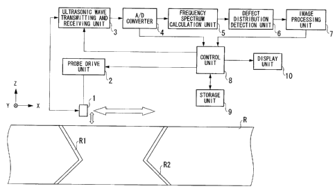
Description of the Reference Numerals
[0024]
1 ... Ultrasonic wave probe, 2 ... Probe drive unit, 3 ... Ultrasonic wave
transmitting
and receiving unit, 4 ... A/D converter, 5 ... Frequency spectrum calculation
unit, 6
... Defect distribution detection unit, 7 ... Image processing unit, 8 ...
Control unit,
9 ... Storage unit, 10 ... Display unit
Best Embodiments for Implementing the Invention
[0025]
An embodiment of the present invention will now be described with reference
CA 02647004 2008-09-23
made to the drawings.
FIG I is a structural block diagram of a defect inspection apparatus according
to
the embodiment of the present invention. Incidentally, the defect inspection
apparatus
quantitatively evaluates a distribution of defects which are caused by creep
damage
within a metal component (inspection material R) including weld portions R1
and R2.
[0026]
As is shown in FIG. 1, this defect inspection apparatus is formed by an
ultrasonic
wave probe 1, a probe drive unit 2, an ultrasonic wave transmitting and
receiving unit 3,
an A/D converter 4, a frequency spectrum calculation unit 5, a defect
distribution
detection unit 6, an image processing unit 7, a control unit 8, a storage unit
9, and a
display unit 10.
[0027]
The ultrasonic wave probe 1 irradiates ultrasonic waves having a frequency
bandwidth of 4 to 20 MHz which are input from the ultrasonic wave transmitting
and
receiving unit 3 onto a surface of an inspection material R via a
predetermined contact
medium. The ultrasonic wave probe 1 also receives ultrasonic waves (i.e.,
scattered
waves) that have been scattered by defects such as voids and cracks present
inside the
inspection material R, and ultrasonic waves (i.e., bottom surface reflected
waves) which
are reflected by a bottom surface (i.e., a rear surface) of the inspection
material R. This
ultrasonic wave probe 1 is also mechanically connected to the probe drive unit
2, and is
moved by the probe drive unit 2 in the X axial direction, namely, along the
surface of the
inspection material R, and is moved up and down in the Z axial direction,
namely, in a
perpendicular direction relative to the surface of the inspection material R.
[0028]
11
CA 02647004 2008-09-23
FIG. 2 shows in detail the structure of an area around the above described
ultrasonic wave probe 1. As is shown in this drawing, the ultrasonic wave
probe I is
gripped by means of a probe holder la, and this probe holder I a is rotatably
connected via
a connecting bolt lb to a scanning unit connection jig 1 c. The scanning unit
connection
jig ]cis connected to a portion (not shown) of the probe drive unit 2 that is
able to move
in the X and Z axial direction. A contact medium Cis coated in advance to a
predetermined thickness on the surface of the inspection material R. A
material having
low viscosity is preferably used for the contact medium C and, for example,
oil having a
density of 1 (g/cm3) or less and a kinematic viscosity of 100 (mm2/s) or less
is preferably
used.
[0029]
Returning to FIG. 1, under the control of the control unit 8, the probe drive
unit 2
causes the ultrasonic wave probe 1 (specifically, including the probe holder
la, the
connecting bolt lb, and the scanning unit connection jig lc) to move in the X
axial
direction, and to move up and down in the Z axial direction. Under the control
of the
control unit 8, the ultrasonic wave transmitting and receiving unit 3
generates ultrasonic
waves having a frequency bandwidth of 4 to 20 MHz, and outputs these to the
ultrasonic
wave probe I at a predetermined timing. The ultrasonic wave transmitting and
receiving
unit 3 also detects scattered waves and bottom surface reflected waves
received by the
ultrasonic wave probe 1, and outputs to the A/D converter 4 irradiation
signals WI that
show the irradiated ultrasonic waves, noise signals WN that show the scattered
waves,
and bottom surface reflected signals W2 that show the bottom surface reflected
waves.
[0030]
The A/D converter 4 converts the irradiation signals W 1, the noise signals
WN,
12
CA 02647004 2008-09-23
and the bottom surface reflected signals W2 which are analog signals into
digital signals,
and outputs these to the frequency spectrum calculation unit 5. The A/D
converter 4
also outputs the digitally converted bottom surface reflected signals W2 to
the control unit
8. The frequency spectrum calculation unit 5 performs FFT processing on the
noise
signals WN based on the irradiation signals W1, the noise signals WN, and the
bottom
surface reflected signals W2 that have been converted into digital signals by
the A/D
converter 4, and outputs to the defect distribution detection unit 6
information which
shows the frequency spectrum obtained from this FFT processing. Note that the
frequency spectrum calculation unit 5 calculates a frequency spectrum by
dividing a time
width Tg from when the irradiation signal W1 is irradiated until the bottom
surface
reflected signal W2 is received into a plurality of time widths Tgl to Tgn,
and then
performing FFT processing on each one of noise signals WN 1 to WNn that are
extracted
in time windows which correspond to the respective divided time widths Tgl to
Tgn (this
process is described in more detail below).
[0031]
The defect distribution detection unit 6 calculates surface area values (Sxl
to
Sxn) of the frequency spectrums of each one of the noise signals WN1 to WNn
based on
the information showing the frequency spectrum which has been input from the
frequency
spectrum calculation unit 5, and calculates a ratio (i.e., a spectrum surface
area ratio)
between the surface area values (Sx I to Sxn) and the surface area value So of
the
frequency spectrum of the noise signal in an inspection material having no
defects which
has been determined by experiment in advance as a value showing the level of
defect
progression, and outputs a spectrum surface area ratio for each one of the
noise signals
WN I to WNn to the image processing unit 7.
13
CA 02647004 2008-09-23
[0032]
The iinage processing unit 7 generates image data showing a relationship
between the positions in the depth direction of the inspection material R
which
correspond to the noise signals WNI to WNn (namely, which correspond to the
respective
divided time widths Tgl to Tgn) and the spectrum surface area ratios based on
the
spectrum surface area ratios of each of the noise signals WNI to WNn which
have been
input from the defect distribution calculation unit 6, and then outputs this
data to the
control unit 8. Note that because the ultrasonic wave probe I is moved in the
X axial
direction by the probe drive unit 2 (described below in more detail), the
image processing
unit 7 generates image data showing the distribution of a two-dimensional
spectrum
surface ratio for the depth direction and the X axial direction of the
inspection material R.
[0033]
The control unit 8 controls the overall operation of this defect inspection
apparatus based on a control program which is stored in the storage unit 9,
and controls
the movement in the X axial direction and the up-down movement in the Z axial
direction
of the ultrasonic wave probe 1 by the probe drive unit 2, and also controls
the irradiation
and the like of ultrasonic waves by the ultrasonic wave transmitting and
receiving unit 3.
The control unit 8 also causes image data which is input from the image
processing unit 7
to be stored in the storage unit 9, and generates display signals that are
used to display the
image data and outputs these to the display unit 10. The control unit 8 also
performs
coupling checks (described below in more detail) based on the bottom surface
reflected
signals W2 which are input from the A/D converter 4. The storage unit 9 stores
the
control program, image data, and other various types of data that are used by
the above
described control unit 8. The display unit 10 displays an image showing the
distribution
14
CA 02647004 2008-09-23
of the two-dimensional spectrum surface ratio for the depth direction and the
X axial
direction of the inspection material R based on display signals input from the
control unit
8.
[0034]
Next, a description will be given of a defect inspection operation of this
defect
inspection apparatus having the above described structure.
[0035]
[Coupling check operation]
Firstly, a coupling check operation will be described. A coupling check is a
process to determine whether or not ultrasonic waves are being irradiated
correctly when
the ultrasonic wave probe I is brought into contact with the surface of the
inspection
material R on which the contact medium C has been coated in advance in order
to
irradiate ultrasonic waves.
[0036]
Assuming that the ultrasonic wave probe 1 is in a position such as that shown
in
FIG. 2, namely, is in an initial state, the control unit 8 controls the probe
drive unit 2 such
that the ultrasonic wave probe I is lowered in the Z axial direction so as to
come into
contact with the surface of the inspection material R via the contact medium
C. At this
time, after the ultrasonic wave probe I has come into contact with the surface
of the
inspection material R, it is further lowered in the Z axial direction by a
particular fixed
distance. By performing this action, as is shown in FIG. 3, because force is
applied in a
direction in which the gap between the probe holder I a and the scanning unit
connection
jig l c becomes smaller, the connecting bolt l b rotates as a single body
together with the
probe holder I a. As a result, the contact medium C is made to properly stick
to the
CA 02647004 2008-09-23
contact surface of the ultrasonic wave probe 1, and air between the ultrasonic
wave probe
1 and the inspection material R can be removed so that ultrasonic waves can be
correctly
irradiated.
[0037]
Note that the distance by which the ultrasonic wave probe I is further lowered
after it has come into contact with the surface of the inspection material R
is desirably set
at a distance which is reached by rotating the ultrasonic wave probe 1
approximately 90 .
It is also desirable for there to be provided a sensor that detects the fact
that the ultrasonic
wave probe I has come into contact with the surface of the inspection material
R, as well
as a mechanism that restores the connecting bolt lb and the probe holder la to
their
original states when the ultrasonic wave probe 1 has been moved away from the
surface
of the inspection material R.
[0038]
Furthermore, in the present embodiment, oil having a density of l (g/cm3) or
less
and a kinematic viscosity of 100 (mm 2/S) or less is preferably used for the
contact
medium C in order to allow the ultrasonic waves to propagate. Generally, in a
nondestructive inspection in which ultrasonic waves are used, a material
having a
comparatively high viscosity such as glycerin paste has been used as the
contact medium.
This has been for the reason that because the propagation efficiency of the
ultrasonic
waves improves as the density and the viscosity of the contact medium
increase, it
becomes possible to maintain a high irradiation intensity of the ultrasonic
waves onto the
inspection material, which makes it possible to reduce the effects of noise
from external
disturbances.
[0039]
16
CA 02647004 2008-09-23
However, when this type of contact medium having a high density and a high
viscosity is used, it is easy for the distance between the ultrasonic wave
probe I and the
surface of the inspection material R to be irregular depending on the position
where the
ultrasonic waves are irradiated. Namely, depending on the position where the
ultrasonic
waves are irradiated, the irradiation intensity varies considerably, so that
it becomes
difficult to accurately detect any defect. Moreover, because the present
defect detection
apparatus quantitatively detects minute defects generated by creep damage, it
is necessary
to keep the distance between the ultrasonic probe 1 and the surface of the
inspection
material R to the minimum and to also keep this distance fixed. Accordingly,
by using
the aforementioned type of oil having a low density and a low viscosity, it is
possible to
form a uniform contact medium having a small film thickness, and to accurately
detect
defects.
[0040]
As has been described above, when the ultrasonic wave probe 1 is brought into
contact with the surface of an inspection material, the control unit 8
controls the
ultrasonic wave transmitting and receiving unit 3 such that ultrasonic waves
are irradiated
into the interior of the inspection material R via the ultrasonic wave probe
1. The
irradiated ultrasonic waves are scattered by defects present in the interior
of the inspection
material R, and scattered waves that are generated by this scattering are
received by the
ultrasonic wave probe 1. In addition, the ultrasonic waves that are reflected
by the
bottom surface (i.e., the rear surface) of the inspection material R (i.e.,
bottom surface
reflected waves) are also received by the ultrasonic wave probe 1.
[0041]
The ultrasonic wave transmitting and receiving unit 3 detects the scattered
waves
17
CA 02647004 2008-09-23
and the bottom surface reflected waves received by the ultrasonic wave probe
1, and
outputs to the A/D converter 4 irradiation signals W 1 that show the
irradiated ultrasonic
waves, noise signals WN that show the scattered waves, and bottom surface
reflected
signals W2 that show the bottom surface reflected waves. These irradiation
signals WI,
noise signals WN, and bottom surface reflected signals W2 are shown in FIG. 4.
Here, if
the ultrasonic waves are not irradiated correctly, the amplitude of the bottom
surface
reflected signals W2 is reduced. Accordingly, if the amplitude of the bottom
surface
reflected signals W2 is smaller than a predetermined threshold value, it can
be determined
that the ultrasonic waves are not being irradiated correctly.
[0042]
Specifically, the A/D converter 4 outputs to the control unit 8 the digitally
converted bottom surface reflected signals W2. The control unit 8 compares the
amplitude of the bottom surface reflected signal W2 with a predetermined
threshold value
and, if the amplitude is less than the threshold value, determines that the
ultrasonic waves
are not being correctly irradiated. This determination result is then
displayed on the
display unit 10, and a user is notified that a coupling error has occurred.
The control
unit 8 then controls the probe drive unit 2 so that the ultrasonic probe 1 is
moved in the X
axial direction, and then once again detects the bottom surface reflected
signals W2.
Note that when the ultrasonic wave probe 1 is being moved in the X axial
direction, it is
desirable for the ultrasonic wave probe 1 to first be temporarily lifted in
the Z axial
direction from the surface of the inspection material R and then moved.
[0043]
As has been described above, the control unit 8 compares the amplitude of the
bottom surface reflected signal W2 with a predetermined threshold value, and
if the
18
CA 02647004 2008-09-23
amplitude is equal to or more than the threshold value, determines that the
ultrasonic
waves are being correctly irradiated and commences the defect scan described
below.
[0044]
[Defect scan]
When the coupling check is ended (at this time, the ultrasonic wave probe I is
in
contact with the surface of the inspection material R via the contact medium
C), the
control unit 8 controls the ultrasonic wave transmitting and receiving unit 3
so that
ultrasonic waves are irradiated into the interior of the inspection material R
from the
ultrasonic wave probe 1. The ultrasonic wave transmitting and receiving unit 3
detects
scattered waves and bottom surface reflected waves received by the ultrasonic
wave
probe 1, and outputs to the A/D converter 4 the irradiation signals W 1 that
show the
irradiated ultrasonic waves, the noise signals WN that show the scattered
waves, and the
bottom surface reflected signals W2 that show the bottom surface reflected
waves (see
FIG. 4). The A/D converter 4 converts the irradiation signals WI, the noise
signals WN,
and the bottom surface reflected signals W2 which are analog signals into
digital signals,
and outputs these to the frequency spectrum calculation unit 5.
[00451
The frequency spectrum calculation unit 5 performs FFT processing on the noise
signals WN based on the irradiation signals WI, the noise signals WN, and the
bottom
surface reflected signals W2 that have been converted into digital signals by
the A/D
converter 4, and outputs to the defect distribution detection unit 6
information which
shows the frequency spectrum obtained from this FFT processing. More
specifically,
the frequency spectrum calculation unit 5 calculates a frequency spectrum by
dividing a
time width Tg from when the irradiation signal W1 is irradiated until the
bottom surface
19
CA 02647004 2008-09-23
reflected signal W2 is received (see FIG 4) into a plurality of time widths
Tgl to Tgn, and
then performing FFT processing on each one of noise signals WNI to WNn that
are
extracted in time windows which correspond to the respective divided time
widths Tgl to
Tgn.
[0046]
Each of these divided time widths Tgl to Tgn corresponds to a position in the
depth direction of the inspection material R. For example, when detecting
defects at a
pitch of 1 mm in the depth direction of the inspection material R, then
assuming a
propagation speed of 5.95 (mm/ s) for the ultrasonic waves inside the
inspection material
R (i.e., the longitudinal wave acoustic velocity in a typical steel material),
this 1 min
distance can be converted into a time width using the following formula.
1 (mm) / 5.95 (mm/lts) x 2 = 0.34 ( s) ... (1)
[0047]
Namely, the respective time widths Tgl to Tgn are obtained by dividing the
time
width Tg equally into 0.34 ( s) units. In this manner, by dividing the time
width Tg into
the respective time widths Tgl to Tgn, and then performing FFT processing on
each of
the noise signals WN1 to WNn that are extracted in time windows that
correspond to the
respective time widths Tgl to Tgn, it is possible to obtain a frequency
spectrum such as
that shown in FIG. 13 (b) at each 1 mm pitch in the thickness direction of the
inspection
material R.
[0048]
The defect distribution detection unit 6 calculates surface area values (Sxl
to
Sxn) of the frequency spectrums for each one of the divided noise signals WNI
to WNn
based on the information showing the frequency spectrum which has been input
from the
CA 02647004 2008-09-23
frequency spectrum calculation unit 5, and calculates a ratio (i.e., a
spectrum surface area
ratio) between the surface area values (Sx 1 to Sxn) and the surface area
value So of the
frequency spectrum of the noise signal in an inspection material having no
defects which
has been determined by experiment in advance, and outputs spectrum surface
area ratios
P1 to Pn for each one of the noise signals WN1 to WNn to the image processing
unit 7.
These spectrum surface area ratios are values that show the level of defect
progression.
[0049]
The image processing unit 7 generates image data showing a relationship
between the positions in the depth direction of the inspection material R
which
correspond to the respective noise signals WN1 to WNn (namely, which
correspond to the
respective divided time widths Tgl to Tgn) and the spectrum surface area
ratios P1 to Pn
based on these spectrum surface area ratios P1 to Pn. Note that, at this
point, because
the image data shows a relationship between the spectrum surface area ratios
P1 to Pn and
the position in the depth direction of the inspection material Rat an
inspection position at
a coordinate located on the X axis, the image data is one-dimensional data.
[0050]
Next, the control unit 8 controls the probe drive unit 2 so that the
ultrasonic
probe I is moved a fixed distance (for example, several millimeters) in the X
axial
direction (i.e., in the scanning direction), and a coupling check is
performed. After this
coupling check, the relationship between the spectrum surface area ratios P1
to Pn and the
position in the depth direction of the inspection material R at a coordinate
on the X axis is
once again detected, and image data is generated. By repeating this type of
operation, as
is shown in FIG. 5, it is possible to obtain image data showing the
distribution of a
spectrum surface area ratio whose vertical axis is the position in the depth
direction of the
21
CA 02647004 2008-09-23
inspection material R and whose horizontal axis is the X axial coordinate,
namely, to
obtain a defect distribution. The control unit 8 generates display signals
that are used to
display the above described image data and outputs these to the display unit
10. Based
on these display signals, the display unit 10 displays an image showing the
distribution of
a two-dimensional spectrum surface ratio for the X axial direction and the
depth direction
of the inspection material R (i.e., the distribution of defects).
[0051]
FIG. 5 shows the defect distribution from the point in time when the
inspection
material R began operating (i.e., from an initial state) until creep damage
(i.e., until the
lifespan consumption rate was 100%). A pattern is fonned that shows the larger
the
value of the spectrum surface area (namely, the greater the level of defect
progression),
the higher the numerical value. Here, numerical values from 1 (a low level of
defect
progression) to 8 (a high level of defect progression) are allocated to show
the level of
defect progression.
[0052]
As is shown in FIG. 5, it is possible to quantitatively evaluate what size of
defect
has occurred, and in what location inside the inspection material R a defect
has occurred
when a particular time has elapsed since the inspection material R started
operating. It
can be seen from FIG. 5 that, in conjunction with the passage of time (i.e.,
with the
progression of creep damage), a large number of defects are generated in the
area around
weld portions R1 and R2.
[0053]
In the present embodiment, ultrasonic waves having amplitude characteristics
such as those shown in FIG. 6 (a) and frequency characteristics such as those
shown in
22
CA 02647004 2008-09-23
FIG. 6 (b) are used. As is shown in FIG. 6 (b), these ultrasonic waves have a
central
frequency of 12 (MHz), and frequencies thereof that are reduced by 20 (dB)
from the
peak intensity are 4 and 20 (MHz), namely, they have a frequency bandwidth of
4 to 20
(MHz). The reason why such ultrasonic waves are used is described below.
[0054]
Firstly, as is described above, in order to obtain a spectrum surface area
ratio at 1
mm intervals in the thickness direction of the inspection material R, it is
necessary to
divide the time width Tg equally into 0.34 ( s). Because the minimum frequency
component that can be contained within this 0.34 ( s) time width is 1/ 0.34 (
s) = 2.95
(MHz), any analysis of frequency components below this 2.95 (MHz) is liable to
contain
considerable errors. Accordingly, it is essential to have a frequency band
larger than
2.95 (MHz). This is the first reason.
[0055]
The second reason will be described using the results of an experiment in
which
the two-dimensional defect distribution was evaluated in the X axial direction
and the
thickness direction of the inspection material R when the frequency band of
the ultrasonic
waves was actually changed. Note that, in this experiment, the distribution of
defects
that were generated as a result of creep damage was evaluated in areas around
weld
portions in an inspection material R such as that shown in FIG 1.
[0056]
FIG. 7 shows the defect distribution from the point in time when the
inspection
material R began operating until creep damage (i.e., until the lifespan
consumption rate
was 100%) when ultrasonic waves having a frequency band of 4 to 8 (MHz) were
used.
FIG. 8 shows the corresponding defect distribution when ultrasonic waves
having a
23
CA 02647004 2008-09-23
frequency band of 4 to 20 (MHz) were used. FIG. 9 shows the corresponding
defect
distribution when ultrasonic waves having a frequency band of 10 to 20 (MHz)
were used.
FIG 10 shows the corresponding defect distribution when ultrasonic waves
having a
frequency band of 15 to 20 (MHz) were used. FIG I1 is a characteristic view
showing a
relationship between the lifespan consumption rate and parameters showing the
scattered
wave intensity when ultrasonic waves having the above described respective
frequency
bands were used.
[0057]
As is shown in FIG. 7 through FIG. 10, irrespective of the frequency band, it
is
possible to obtain the same defect distribution as that shown in FIG. 5 in
accordance with
the rise in the lifespan consumption rate. However, as is shown in FIG 11, it
can be seen
that in the case of ultrasonic waves having a frequency band of 10 to 20 (MHz)
and those
having a frequency band of 15 to 20 (MHz), there is only a small amount of
change in the
parameters showing the scattered wave intensity for the lifespan consumption
rate, and
the detection sensitivity of the scattered waves is poor.
[0058]
In contrast, in the case of ultrasonic waves having a frequency band of 4 to 8
(MHz), it can be seen from FIG 11 that there is excellent detection
sensitivity, however,
as is shown in FIG 7, there is also considerable material noise from outside
the areas
around the weld portions, and it is difficult to acquire significant noise
signals (i.e., noise
signals that are generated by defects which are caused by creep damage).
Accordingly,
in the present embodiment, it is possible to acquire significant noise signals
based on
these experiment results, so that it was decided to use ultrasonic waves
having a
frequency band of 4 to 20 (MHz) which also have excellent detection
sensitivity towards
24
CA 02647004 2008-09-23
scattered waves.
[0059]
As has been described above, according to the present embodiment, it is
possible
to quantitatively evaluate the distribution of defects generated inside an
inspection
material R, and the present embodiment is extremely effective when a process
from the
occurrence of a defect to the failure of the inspection material is being
examined.
[0060]
Note that the present invention is not limited to the above described
embodiment
and, for example, the variant examples described below may also be considered.
[0061]
(1) In the above described embodiment, the distribution of defects generated
in the
interior of an inspection material R is evaluated quantitatively, however, the
present
invention is not limited to this and it is also possible to employ a structure
in which there
is provided a function (i.e., a damage lifespan determination device) that
predicts the
remaining lifespan of the inspection material R based on the results of a
defect
distribution evaluation of this type. Specifically, as is the case
conventionally, it is
possible to predict the remaining lifespan from the remaining lifespan curve
shown in FIG
14.
[0062]
(2) In the above described embodiment, the defect distribution is detected at
1 mm
intervals in the thickness direction of the inspection material R, however,
the present
invention is not limited to this and it is also possible to appropriately
modify the defect
detection pitch in the thickness direction. However, if the defect detection
pitch in the
thickness direction is modified, then it is necessary to adjust the frequency
of the
CA 02647004 2008-09-23
ultrasonic waves being used and also the time width divisions of the time
width Tg in
accordance with the modification.
[0063]
(3) In the above described embodiment, a description is given of a case in
which
defects that are caused by creep damage are detected, however, the present
invention is
not limited to this and the present defect inspection apparatus can also be
used to detect
defects such as voids and cracks and the like that are generated by hydrogen
corrosion
and other causes.
26