Note: Descriptions are shown in the official language in which they were submitted.
CA 02647233 2010-04-27
ANTI-FUSE MEMORY CELL
FIELD OF THE INVENTION
[0002] The present invention relates generally to non-volatile memory. More
specifically, the invention is directed to anti-fuse memory cell structures.
BACKGROUND OF THE INVENTION
[0003] Over the past 30 years, anti-fuse technology has attracted significant
attention
of many inventors, IC designers and manufacturers. An anti-fuse is a structure
alterable to a
conductive state, or in other words, an electronic device that changes state
from not
conducting to conducting. Equivalently, the binary states can be either one of
high resistance
and low resistance in response to electric stress, such as a programming
voltage or current.
There have been many attempts to develop and apply anti-fuses in
microelectronic industry,
but the most successful anti-fuse applications to date can be seen in FGPA
devices
TM TM
manufactured by Actei and Quicklogic, and redundancy or option programming
used in
TM
DRAM devices by Micron.
[0004] A summary of the progression of anti-fuse development follows as
evidenced
by issued United States patents.
[0005] Anti-fuse technology development started with U.S. Patent No.
3,423,646,
which disclosed a thin film formable diode PROM built as an array of
horizontal and vertical
conductors with a thin dielectric (aluminium oxide) between the conductors, at
their
crossings. Such NVM memory was programmed through perforation of the
dielectric in some
of the crossings. A formable diode would act as an open circuit until a
voltage of sufficient
- 1 -
CA 02647233 2008-12-23
WO 2008/151429 PCT/CA2008/001122
magnitude and duration is applied to the crossing to cause forming of the
aluminum oxide
intermediate layer at which time device would act as a tunnelling diode.
[0006] U.S. Patent No. 3,634,929 disclosed an inter-metal semiconductor anti-
fuse
array, the structure of the anti-fuse consisting of a thin dielectric
capacitor (AI02, Si02 or
Si3N4) utilizing two (Al) conductors located above and connected to the
semiconductor
diode.
[0007] A programmable dielectric ROM memory structure using a MOS capacitor
and
a MOS switching element was shown in U.S. Patent No. 4,322,822 (McPherson).
This cell
was formed as a standard gate-oxide-over-substrate capacitor having a gate
connected to a
MOS transistor using a buried contact. In order to lower the oxide breakdown
voltage, which
needed to be smaller for the anti-fuse capacitor then for the MOS switch, a V-
shaped grove
in the capacitor area was proposed. Since the capacitor was formed between the
poly gate
and the grounded p-type substrate, the rupture voltage had to be applied to
the capacitor
through an access transistor. The Gate/Drain and Gate/Source edges of the
access
transistors were located at the second field oxide, much thicker then the gate
oxide in the
channel area, which greatly improved Gate/S-D breakdown voltage.
[0008] U.S. Patent No. 4,507,757 (McElroy) proposed a method for lowering gate
oxide breakdown voltage through avalanche junction breakdown. Although the
original
McElroy ideas evolved around using gated diodes to locally induce avalanche
breakdown,
which in turn lowered dielectric rupture voltage by enhanced electron
tunnelling, he actually
introduced or embodied other and perhaps more important elements to anti-fuse
technology:
(a) Dual gate oxide anti-fuse: access transistor gate oxide thicker then anti-
fuse dielectric.
McElroy's dual gate oxide process steps are: initial gate oxidation, etching
areas for thinner
gate oxide and subsequent gate oxidation. This procedure is now used in
standard CMOS
technologies for "I/O" and "IT" devices. (b) A "common-gate" (planar DRAM
like) anti-fuse
connection where access transistor connects to anti-fuse diffusion (Drain)
node and all the
anti-fuse gates are connected together. This is opposite to McPherson
arrangement and
results in much denser cell since the buried contact is eliminated. (c)
Limiting resistor
between common anti-fuse gate and external ground. (d) Two-terminal anti-fuse
MOS device
(a half transistor): McElroy concluded that only two terminals are needed in
anti-fuse
capacitor: D and G. The Source is not really needed for anti-fuse programming
or operation
and can be fully isolated from the active area. The bulk connection does not
play any role
-2-
CA 02647233 2010-04-27
either except for the avalanche breakdown. So the source role is limited to
collecting carriers
from the avalanche breakdown should the local substrate potential increase to
forward bias
the emitter of a parasitic n-p-n device formed by D, B and S.
[0009] It wasn't until 1985 when U.S. Patent No. 4,543,594 (Mohsen) proposed
an
anti-fuse design suitable for redundancy repair. As such application requires
much lower
density than PROM, it was easier to supply external high voltage necessary to
rupture the
oxide without actually passing this voltage through the access transistors.
Mohsen's anti-fuse
structure consisted of a thin oxide (50-150A Si02) polysilicon capacitor over
a doped region.
He believed that silicon from the substrate or silicon from the electrode
where a polysilicon
electrode is used melts into pin holes in the insulative layer to provide the
conductor, and his
test data showed that where the oxide layer is approximately 100A thick and
has an area
between 10 to 500 um2, fusion occurred at a voltage of 12 to 16 volts. The
current required to
cause this fusion is less than 0.1 uA/um2 of capacitor area, and the resulting
fused link has a
resistance of approximately 0.5 to 2K ohms. A link, once fused, can handle
currents of up to
100 milliamps at room temperature for approximately one second before it heals
to an open
fuse. Taking into account electron migration wear-out, the predicted wear-out
lifetime of a
link, once fused, is substantially greater than 3E8 hours.
[0010] The possibility of anti-fuse self-healing under current stress appeared
to be
the main roadblock for application of this technology in such areas like
PROMs, PLDs and
FPGAs, where constant fuse stress was required. The anti-fuse healing problem
was
resolved later by Mohsen and others at Actel in U.S. Patent No. 4,823,181.
Actel teaches the
way to implement a reliable programmable low impedance anti-fuse element by
using an
ONO structure instead of silicon dioxide. Actel's method required an ohmic
contact after
dielectric rupture. This was achieved either by using heavily doped diffusion,
or by putting an
ONO dielectric between two metal electrodes (or silicide layers). The
necessity of an Arsenic
doped bottom diffusion electrode was revised later in U.S. Patent No.
4,899,205, where it
was allowed for either top-poly or bottom-diffusion to be highly doped.
[0011] U.S. Patent No. 5,019,878 taught that if the drain is silicided, the
application of
a programming voltage in the range of ten to fifteen volts from the drain to
the source reliably
forms a melt filament across the channel region. A gate voltage may be applied
to control the
TM
specific transistors to melt. IBM aiscovered similar effect by proposing a
channel anti-fuse in
U.S. Patent No. 5,672,994. They discovered that with 0.5um technology, the
BVDSS for the
-3-
CA 02647233 2010-04-27
nmos transistor is not only in the order of 6.5V, but once the S-D punch
through occurs it
creates permanent damage resulting in few kilo ohms leakage between the source
and the
drain.
[0012] U.S. Patent Nos. 5,241,496 and 5,110,754 to Micron, disclosed a DRAM
cell
based anti-fuse (trench and stack). In 1996, Micron introduced a well-to-gate
capacitor as an
anti-fuse in U.S. Patent No. 5,742,555. U.S. Patent No. 6,087,707 proposed an
N-Well
coupled anti-fuse as a way to eliminate undercut defects associated with
polysilicon etching.
U.S. Patent Publication No. 2002/0027,822 proposed a similar anti-fuse
structure, but with n+
regions removed to create an asymmetrical ("unbalanced") high voltage access
transistor
using the N-well as a drain electrode.
[0013] U.S. Patent No. 6,515,344 proposed a range of P+/N+ anti-fuse
configurations, implemented using a minimum size gate between two opposite
type diffusion
reqions.
[0014] Nmos anti-fuses built in an isolated P-well using a standard Deep N-
Well process is
known in the art. Another variant of Deep N-Well based anti-fuses is disclosed
in U.S. Patent
No. 6, 611, 040.
[0015] U.S. Patent Publication Nos. 2002,0074,616 and 2004,0023,440 disclose
other Deep N-Well anti-fuses. These anti-fuses consisted of a capacitor
featuring direct
tunnelling current rather then Fowler Nordheim current. These applications
confirm that anti-
fuse performance is generally improved for thinner gate oxide capacitors
(approx 20A, which
is typical for transistors in 0.13um process).
[0016] U.S. Patent No. 6,580,145 disclosed a new version of a traditional anti-
fuse
structure utilizing dual gate oxides, with the thicker gate oxide being used
for nmos (or pmos)
access transistors and the thinner gate oxide for the capacitor. The N-Well
(or P-Well) is
used as a bottom plate of the anti-fuse capacitor.
[0017] The idea of creating a source drain short through the gate by
separately
breaking the S-G and D-G dielectric regions of the transistor is disclosed in
U.S. Patent No.
6,597,234.
[0018] U.S. Patent Publication No. 2004,0004,269 disclosed an anti-fuse built
from a
MOS transistor having gate connected to the gate of a capacitor, degenerated
by a thinner
-4-
CA 02647233 2009-08-24
gate oxide and heavy doping under the channel through additional implantation
(a diode).
The rupture voltage is applied to a bottom plate of the capacitor,
[D019] In U.S. Patent No. 6,667,602 (Pang) Pang attempts to improve a classic
planar DRAM-like anti-fuse array by introducing "row program lines" which
connect to the
capacitors and run parallel to the word lines, If decoded, the row program
lines can minimize
exposure of access transistors to a high programming voltage, which would
otherwise occur
through already programmed cells. Pang and Fong further improve their array in
U.S. Patent
No. 6,671,040 by adding a variable voltage controlling programming current,
which allegedly
controls the degree of gate oxide breakdown, allowing for multilevel or analog
storage
applications.
[0020] Most recently, U.S. Patent Publication No. 2003/0202376 (Pang) shows a
memory array using a single transistor structure, In the proposed memory cell,
Pang
eliminates the LDD diffusion from a regular NMOS transistor. A crass-point
array structure is
formed of horizontal active area (S/D) stripes crossing vertical poly gate
stripes. Drain
contacts are shared between neighbouring cells and connected to horizontal
wordlines.
Source regions are also shared and left floating. Peng assumes that if the LDD
diffusion is
omitted, the gate oxide breakdown location will be far enough from the drain
area and a local
N+ region will be created rather than D-G (drain-gate) short. If such a region
was created, the
programmed cells could be detected by positively biasing the gate and sensing
the gate to
drain current. In order to reduce the G-D or S-D (source-drain) short
probability, Peng
proposes increasing gate oxide thickness at the G-D and S D edges through
modification of
a gate sidewall oxidation process. Peng's array requires that both source and
drain regions
be present in the memory cells, row wordlines coupled to transistor drain
regions, and the
column bitlines formed from transistor gates. Such an unusual connection must
be very
specific to Peng's programming and reading method, requiring a decoded high
voltage (sv in
1.8V process) applied to all drain lines except for the one to be programmed.
The decoded
high voltage (8V) is applied to the gates of the column to be programmed,
while the other
gates are kept at 3-3V.
(00211 Although Pang achieves a cross-point memory architecture, his array
requires
CMOS process modifications (LDD elimination, thicker gate oxide at the edge)
and has the
following disadvantages. (a) All row decoders, column decoders and sense
amplifiers must
switch a wide range of voltages: 8V/3.3V/OV or 8V/1.BV/OV. (b) During a
program operation,
-5-
CA 02647233 2009-08-24
the 3.3V column drivers are effectively shorted to 8V row drivers or OV
drivers through
programmed cells. This puts many limits on the array size, affects driver size
and impacts
reliability and effectiveness of programming. (c) Every program operation
requires that all the
array active areas (except for the programmed row) are biased at By. This
leads to large
N++ junction leakage current, and again limits array size. (d) The gate oxide
breaking spot is
assumed to be located far enough from the drain area so the punch through is
not happening
at 8V bias- At the same time, the transistor must operate correctly at 1.8V
biasing -
connecting to the channel area. This is not achievable without significant
process
modification. (e) Peng assumes that the gate oxide will not break on the
source or drain edge
if the LOD is not present. It is however known in the art that the SID edges
are the most likely
locations for the oxide breakdown because of defects and electric field
concentration around
sharp edges.
[0022] Pang attempts to solve some of the high voltage switching problems In
U.S.
Patent Publication No. 200310206467. The high blocking voltage on wordlines
and bitlines is
now replaced with "floating" wordlines and bitlines, and restrictions on the
distance from the
channel to the source and drain regions has been changed. Although floating
wordlines and
bitlines may ease problems with high voltage switching, they do not solve any
of the above
mentioned fundamental problems. Additionally they introduce severe coupling
problems
between the switched and the floating lines.
[0023] Today, anti-fuse developments concentrate around 3-dimentional thin
film
structures and special inter-metal materials. All these anti-fuse technologies
require
additional processing steps not available In standard CMOS process,
prohibiting anti-fuse
applications in typical VLSI and ASIC designs, where programmability could
help overcome
problems with ever shrinking device life cycles and constantly rising chip
development costs.
Therefore there is an apparent need in the industry for a reliable anti-ruse
structures utilizing
standard CMOS process.
(0024] All the prior art anti-fuse cells and arrays either require special
processing
steps or suffer from high voltage exposure of MOS switching elements, leading
to
manufacturability and reliability problems. They are also limited to low
density memory
applications, with the exception of Pang's single transistor cell, which in
turn has very
doubtful manufacturability.
-6-
CA 02647233 2008-12-23
WO 2008/151429 PCT/CA2008/001122
[0025] It is, therefore, desirable to provide a simple and reliable, high
density, anti-
fuse array architecture suitable for implementation in standard CMOS
technology, without
any additional processing steps.
SUMMARY OF THE INVENTION
[0026] It is an object of the present invention to obviate or mitigate at
least one
disadvantage of the previous anti-fuse arrays by providing an anti-fuse memory
cell having
high reliability by minimizing a thin gate oxide area of a variable thickness
gate oxide formed
between a polysilicon gate and the active area of the substrate.
[0027] In a first aspect, the present invention provides an anti-fuse
transistor formed
on a substrate. The anti-fuse transistor includes a polysilicon gate, a
diffusion region, a field
oxide region, and a variable thickness gate oxide. The polysilicon gate is
formed over a
channel region having a channel length. The diffusion region is proximate to a
first end of the
channel region. The field oxide region is proximate to a second end of the
channel region.
The variable thickness gate oxide is formed between the polysilicon gate and
the substrate.
The variable thickness gate oxide has a first thick gate oxide segment, a
second thick gate
oxide segment and thin gate oxide portion. The first thick gate oxide segment
extends from
the first end of the channel region to a first predetermined distance of the
channel length.
The second thick gate oxide segment is adjacent the first thick gate oxide
segment, and
extends from the first end of the channel region to a second predetermined
distance of the
channel length. The first thick gate oxide segment and the second gate oxide
segment are
sized for covering the channel region. The thin gate oxide portion extends
from the second
predetermined distance to the second end of the channel region.
[0028] According to an embodiment of the present aspect, the second thick gate
oxide segment includes a third gate oxide segment being triangular in shape
adjacent to the
first thick gate oxide segment, the second predetermined distance being
defined by a
diagonal edge of the third gate oxide segment. In another embodiment, the
first
predetermined distance is between the first end of the channel region and the
second end of
the channel region, and the second predetermined distance can be between the
first
predetermined distance and the first end of the channel region. Furthermore,
the first
predetermined distance can correspond to the second end of the channel region,
and the
-7-
CA 02647233 2008-12-23
WO 2008/151429 PCT/CA2008/001122
second predetermined distance is between the first predetermined distance and
the first end
of the channel region.
[0029] In yet another embodiment of the present aspect, the channel region has
a
varying width between the first end and the second end of the channel region.
In one
embodiment, the anti-fuse transistor further includes a second diffusion
region spaced from
the first diffusion region to define a second channel region, a second
polysilicon gate over
the second channel region, and a thick gate oxide between the polysilicon gate
and the
second channel region, the thick gate oxide having a thickness identical to
the first thick gate
oxide segment. In the present embodiment, the first thick gate oxide segment
includes a first
sub-segment extending from the first end of the channel region to a third
predetermined
distance, and a second sub-segment extending from the first end of the channel
to the first
predetermined distance. The third predetermined distance can be between the
first end of
the channel region and the first predetermined distance. According to further
aspects of the
present embodiment, the first predetermined distance and the second
predetermined
distance are identical. The second thick gate oxide segment includes a third
sub-segment
extending from the first end of the channel region to a fourth predetermined
distance, and a
fourth sub-segment extending from the first end of the channel to the second
predetermined
distance. The fourth predetermined distance is between the first end of the
channel region
and the second predetermined distance. The first predetermined distance can be
identical to
the second predetermined distance, or the third predetermined distance and the
second
predetermined distance can be identical, or the second predetermined distance
can be
between the first predetermined distance and the fourth predetermined
distance.
[0030] In a further embodiment of the present aspect, the second thick gate
oxide
segment includes a first sub-segment extending from the first end of the
channel region to a
third predetermined distance, and a second sub-segment extending from the
first end of the
channel to the second predetermined distance, the third predetermined distance
being
between the first end of the channel region and the second predetermined
distance. The
second sub-segment includes a third gate oxide segment being triangular in
shape adjacent
to the first thick gate oxide segment, the second predetermined distance being
defined by a
diagonal edge of the third gate oxide segment.
[0031] In yet another embodiment, the thin gate oxide portion has at least one
dimension less than a minimum feature size of a process technology. In another
-8-
CA 02647233 2008-12-23
WO 2008/151429 PCT/CA2008/001122
embodiment, the anti-fuse transistor further includes a second diffusion
region spaced from
the first diffusion region to define a second channel region, a second
polysilicon gate over
the second channel region, and a thick gate oxide between the polysilicon gate
and the
second channel region. The thick gate oxide has a thickness identical to the
first thick gate
oxide segment. In the present embodiment, the second diffusion region has a
variable width,
the channel region has a first width corresponding to a narrow section of the
second diffusion
region and a second width corresponding to a wide section of the second
diffusion region.
[0032] In a second aspect, the present invention provides a non-volatile
memory cell
formed on a substrate. The non-volatile memory cell includes an anti-fuse
transistor and an
access transistor. The anti-fuse transistor has a first polysilicon gate over
a variable
thickness gate oxide, the variable thickness gate oxide having a thick gate
oxide portion and
a thin gate oxide portion. The access transistor has a second polysilicon gate
over a fixed
thickness gate oxide, the fixed thickness gate oxide and the thick gate oxide
portion being
substantially identical in thickness. According to an embodiment of the
present aspect, the
thick gate oxide portion includes a first thick gate oxide segment, a second
thick gate oxide
segment, and a thin gate oxide portion. The first thick gate oxide segment
extends from a
first end of a channel region to a second end of the channel region, the first
thick gate oxide
segment having a first width less than the channel width. The second thick
gate oxide
segment is adjacent the first thick gate oxide segment, which extends from the
first end of
the channel region to a predetermined distance of the channel length. The
second thick gate
oxide segment has a second width substantially equal to the difference between
the channel
width and the first width. The thin gate oxide portion extends from the
predetermined
distance to the second end of the channel region. In the present embodiment,
the non-
volatile memory cell further includes a third gate oxide segment being
triangular in shape
adjacent to the first thick gate oxide segment and the second thick gate oxide
segment.
[0033] In a third aspect, the present invention provides anti-fuse transistor
formed on
a substrate. The anti-fuse transistor has a polysilicon gate over a channel
region, a diffusion
region, a field oxide region, and a variable thickness gate oxide. The
polysilicon gate is
formed over the channel region,which has a channel length and a channel width.
The
diffusion region is proximate to a first end of the channel region and the
field oxide region is
proximate to a second end of the channel region. The variable thickness gate
oxide is formed
between the polysilicon gate and the substrate, and has a thick gate oxide
portion and a thin
-9
CA 02647233 2008-12-23
WO 2008/151429 PCT/CA2008/001122
gate oxide portion. The thin gate oxide portion has dimensions less than a
minimum feature
size of a process technology.
[0034] According to embodiments of the present aspect, the thin gate oxide
portion is
rectangular in shape, such that a first side and a second side of the
rectangle are bound by
the thick gate oxide portion and a third side and a fourth side of the
rectangle are bound by
the channel region. Alternately, the thin gate oxide portion is triangular in
shape, such that a
first side and a second side of the triangle are bound by the channel region
and a diagonal
side of the triangle is bound by the thick gate oxide portion.
[0035] In a fourth aspect, the present invention provides a method of forming
an anti-
fuse transistor having a thick gate oxide area and a thin gate oxide area
underneath a
polysilicon gate. The method includes a) growing an intermediate oxide in an
active area of
the anti-fuse transistor; b) removing the intermediate oxide from an area of
the active area
defined by an oxide definition mask having a grade equal to or higher than a
source/drain
implant definition mask; and, c) growing a thin oxide in the area defined by
the oxide
definition mask. In embodiments of the present aspect, the oxide definition
mask has a grade
corresponding to a diffusion implant mask, and the oxide definition mask
includes an opening
overlapping an active area corner underneath the polysilicon gate to define
the area. The
opening can be rectangular in shape and dimensioned to have each corner
overlap active
area corners corresponding to at least two different anti-fuse transistors.
[0036] In further embodiments of the present aspect, the oxide definition mask
includes an opening having an edge angled relative to the polysilicon gate
overlapping an
active area corner underneath the polysilicon gate to define the area. The
opening can
include a diamond shape dimensioned to have each edge overlap active area
corners
corresponding to at least two different anti-fuse transistors. Alternately,
the oxide definition
mask can include a rectangular shape having an edge overlapping the active
area
underneath the polysilicon gate to define the area, the area having a width
corresponding to
a width of the active area.
[0037] According to embodiments of the present aspect, the step of removing
can
include aligning the oxide definition mask with an alignment machine using a
highest
accuracy tolerance, and the step of growing thin oxide can include growing the
thin oxide
over the intermediate oxide to form the thick gate oxide area, where the step
of growing thin
-10-
CA 02647233 2008-12-23
WO 2008/151429 PCT/CA2008/001122
oxide includes growing the thin oxide over the intermediate oxide to form a
gate oxide for an
access transistor adjacent to the anti-fuse transistor.
[0038] Other aspects and features of the present invention will become
apparent to
those ordinarily skilled in the art upon review of the following description
of specific
embodiments of the invention in conjunction with the accompanying figures.
BRIEF DESCRIPTION OF THE DRAWINGS
[0039] Embodiments of the present invention will now be described, by way of
example only, with reference to the attached Figures, wherein:
Fig. 1 is a circuit diagram of a DRAM-type anti-fuse cell;
Fig. 2 is a planar layout of the DRAM-type anti-fuse cell of Figure 1;
Fig. 3 is a cross-sectional view of the DRAM-type anti-fuse cell of Figure 2
along line x-x;
Fig. 4 is a cross-sectional view of an anti-fuse transistor according to an
embodiment of the present invention;
Fig. 5a is a planar layout of the anti-fuse transistor of Figure 4;
Fig. 5b is a planar layout of the anti-fuse transistor of Figure 4 showing an
alternate OD2 mask configuration;
Fig. 6 is a flow chart of a method for forming a variable thickness gate oxide
for the anti-fuse transistor of the present invention;
Fig. 7a-7c illustrate the formation of the variable thickness gate oxide in
accordance with steps of the flow chart of Figure 6;
Fig. 8a is a planar layout of an anti-fuse transistor according to an
embodiment of the present invention;
Fig. 8b is a cross-sectional view of the anti-fuse transistor of Fig. 8a taken
along line A-A;
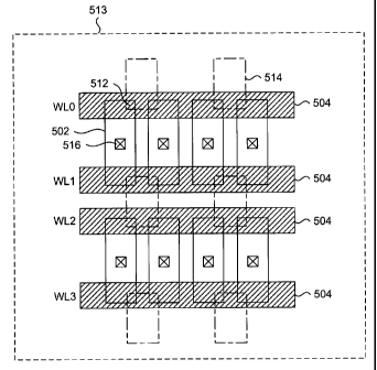
Fig. 9 is an enlarged planar layout of the anti-fuse transistor of Fig. 8a;
Fig. 10 is a planar layout of a memory array using the anti-fuse transistor of
Fig. 8a according to an embodiment of the present invention;
Fig. 11 is an enlarged planar layout of an anti-fuse transistor, according to
another embodiment of the present invention;
-11-
CA 02647233 2008-12-23
WO 2008/151429 PCT/CA2008/001122
Fig. 12 is a planar layout of a memory array using the anti-fuse transistor of
Figure 11 according to an embodiment of the present invention;
Fig. 13a is a planar layout of a two-transistor anti-fuse memory cell
according
to an embodiment of the present invention;
Fig. 13b is a cross-sectional view of the two-transistor anti-fuse memory cell
of
Fig. 13a taken along line B-B;
Fig. 14 is a planar layout of a memory array using the two-transistor anti-
fuse
memory cell of Figure 13a and 13b, according to an embodiment of the present
invention;
Fig. 15 is a planar layout of a memory array using the two-transistor anti-
fuse
memory cell according to an alternate embodiment of the present invention;
Fig. 16-20 are planar layouts of alternate anti-fuse memory cells, according
to
embodiments of the present invention; and
Fig. 21-24 are planar layouts of alternate two-transistor anti-fuse memory
cells, according to embodiments of the present invention.
DETAILED DESCRIPTION
[0040] Generally, the present invention provides a variable thickness gate
oxide anti-
fuse transistor device that can be employed in a non-volatile, one-time-
programmable (OTP)
memory array application. The anti-fuse transistor can be fabricated with
standard CMOS
technology, and is configured as a standard transistor element having a source
diffusion,
gate oxide and a polysilicon gate. The variable gate oxide underneath the
polysilicon gate
consists of a thick gate oxide region and a thin gate oxide region, where the
thin gate oxide
region acts as a localized breakdown voltage zone. A conductive channel
between the
polysilicon gate and the channel region can be formed in the localized
breakdown voltage
zone during a programming operation. In a memory array application, a wordline
read current
applied to the polysilicon gate can be sensed through a bitline connected to
the source
diffusion, via the channel of the anti-fuse transistor. More specifically, the
present invention
provides an effective method for utilizing split channel MOS structures as an
anti-fuse cell
suitable for OTP memories.
-12-
CA 02647233 2008-12-23
WO 2008/151429 PCT/CA2008/001122
[0041] In the following description the term MOS is used to denote any FET or
MIS
transistor, half-transistor or capacitor structure. In order to simplify the
description of the
embodiments, references to gate oxides from this point forward should be
understood to
include dielectric materials, oxide, or a combination of oxide and dielectric
materials.
[0042] As previously discussed, a DRAM-type memory array using a planar
capacitors as an anti-fuse instead of as a storage capacitor is already known,
as
demonstrated in U.S. Patent No. 6,667,902. Figure 1 is a circuit diagram of
such a memory
cell, while Figures 2 and 3 show the planar and cross-sectional views
respectively, of the
known anti-fuse memory cell of Figure 1. The memory cell of Figure 1 includes
a pass, or
access transistor 10 for coupling a bitline BL to a bottom plate of anti-fuse
device 12. A
wordline WL is coupled to the gate of access transistor 10 to turn it on, and
a cell plate
voltage Vcp is coupled to the top plate of anti-fuse device 12 for programming
anti-fuse
device 12.
[0043] It can be seen from Figures 2 and 3 that the layout of access
transistor 10 and
anti-fuse device 12 is very straight-forward and simple. The gate 14 of access
transistor 10
and the top plate 16 of anti-fuse device 12 are constructed with the same
layer of polysilicon,
which extend across active area 18. In the active area 18 underneath each
polysilicon layer,
is formed a thin gate oxide 20, also known as a gate dielectric, for
electrically isolating the
polysilicon from the active area underneath. On either side of gate 14 are
diffusion regions
22 and 24, where diffusion region 24 is coupled to a bitline. Although not
shown, those of skill
in the art will understand that standard CMOS processing, such as sidewall
spacer formation,
lightly doped diffusions (LDD) and diffusion and gate silicidation, can be
applied. While the
classical single transistor and capacitor cell configuration is widely used, a
transistor-only
anti-fuse cell is further desirable due to the semiconductor array area
savings that can be
obtained for high-density applications. Such transistor-only anti-fuses must
be reliable while
simple to manufacture with a low cost CMOS process.
[0044] According to an embodiment of the present invention, Figure 4 shows a
cross-
sectional view of an anti-fuse transistor that can be manufactured with any
standard CMOS
process. In the presently shown example, the anti-fuse transistor is almost
identical to a
simple thick gate oxide, or input/output MOS transistor with one floating
diffusion terminal.
The disclosed anti-fuse transistor, also termed a split-channel capacitor or a
half-transistor,
can be reliably programmed such that the fuse link between the polysilicon
gate and the
-13-
CA 02647233 2008-12-23
WO 2008/151429 PCT/CA2008/001122
substrate can be predictably localized to a particular region of the device.
The cross-section
view of Figure 4 is taken along the channel length of the device, which in the
presently
described embodiment is a p-channel device. Those of skill in the art will
understand that the
present invention can be implemented as an n-channel device.
[0045] Anti-fuse transistor 100 includes a variable thickness gate oxide 102
formed
on the substrate channel region 104, a polysilicon gate 106, sidewall spacers
108, a field
oxide region 109 a diffusion region 110, and an LDD region 114 in the
diffusion region 110. A
bitline contact 116 is shown to be in electrical contact with diffusion region
110. The variable
thickness gate oxide 102 consists of a thick oxide and a thin gate oxide such
that a portion of
the channel length is covered by the thick gate oxide and the remaining
portion of the
channel length is covered by the thin gate oxide. Generally, the thin gate
oxide is a region
where oxide breakdown can occur. The thick gate oxide edge meeting diffusion
region 110
on the other hand, defines an access edge where gate oxide breakdown is
prevented and
current between the gate 106 and diffusion region 110 is to flow for a
programmed anti-fuse
transistor. While the distance that the thick oxide portion extends into the
channel region
depends on the mask grade, the thick oxide portion is preferably formed to be
at least as
long as the minimum length of a high voltage transistor formed on the same
chip.
[0046] In a preferred embodiment, the diffusion region 110 is connected to a
bitline
through a bitline contact 116, or other line for sensing a current from the
polysilicon gate 106,
and can be doped to accommodate programming voltages or currents. This
diffusion region
110 is formed proximate to the thick oxide portion of the variable thickness
gate oxide 102.
To further protect the edge of anti-fuse transistor 100 from high voltage
damage, or current
leakage, a resistor protection oxide (RPO), also known as a salicide protect
oxide, can be
introduced during the fabrication process to further space metal particles
from the edge of
sidewall spacer 108. This RPO is preferably used during the salicidiation
process for
preventing only a portion of diffusion region 110 and a portion of polysilicon
gate 106 from
being salicided.
[0047] It is well known that salicided transistors are known to have higher
leakage
and therefore lower breakdown voltage. Thus having a non-salicided diffusion
region 110 will
reduce leakage. Diffusion region 110 can be doped for low voltage transistors
or high voltage
transistors or a combination of the two resulting in same or different
diffusion profiles.
-14-
CA 02647233 2008-12-23
WO 2008/151429 PCT/CA2008/001122
[0048] A simplified plan view of the anti-fuse transistor 100 is shown in
Figure 5a.
Bitline contact 116 can be used as a visual reference point to orient the plan
view with the
corresponding cross-sectional view of Figure 4. The active area 118 is the
region of the
device where the channel region 104 and diffusion region 110 is formed, which
is defined by
an OD mask during the fabrication process. The dashed outline 120 defines the
areas in
which the thick gate oxide is to be formed via an OD2 mask during the
fabrication process.
More specifically, the area enclosed by the dashed outline 120 designates the
regions where
thick oxide is to be formed. OD simply refers to an oxide definition mask that
is used during
the CMOS process for defining the regions on the substrate where the oxide is
to be formed,
and OD2 refers to a second oxide definition mask different than the first.
Details of the
CMOS process steps for fabricating anti-fuse transistor 100 will be discussed
later.
According to an embodiment of the present invention, the thin gate oxide area
bounded by
edges of the active area 118 and the rightmost edge of the OD2 mask, is
minimized. In the
presently shown embodiment, this area can be minimized by shifting the
rightmost OD2
mask edge towards the parallel edge of active area 118.
[0049] Figure 5b is an alternate illustration of anti-fuse 100 of Figure 5a.
In Figure 5a,
the OD2 mask 120 is shown as a large area that may extend to cover the entire
memory
array. As previously discussed, OD2 mask 120 defines the areas in which the
thick gate
oxide is to be formed. Formed within OD2 mask 120 are openings 121 defining
areas where
no thick gate oxide is to be formed. Instead, thin gate oxide will be grown in
the area defined
by openings 121. Those skilled in the art will understand that in a memory
array configuration
where a plurality of anti-fuse memory cells 100 are arranged in a row, one
rectangular
opening can overlap all the memory cells to define the thin gate oxide area
for each active
area 118.
[0050] Programming of anti-fuse transistor 100 is based on gate oxide
breakdown to
form a permanent link between the gate and the channel underneath. Gate oxide
breakdown
conditions (voltage or current and time) depend primarily on i) gate
dielectric thickness and
composition, ii) defect density, and iii) gate area, gate/diffusion perimeter.
The combined
thick and thin gate oxide of anti-fuse transistor 100 results in a locally
lowered gate
breakdown voltage, in particular an oxide breakdown zone, in the thin gate
oxide portion of
the device. In otherwords, the disclosed structure assures that the oxide
breakdown is limited
to the thinner gate oxide portion.
-15-
CA 02647233 2008-12-23
WO 2008/151429 PCT/CA2008/001122
[0051] Additionally, the anti-fuse transistor embodiments of the present
invention take
advantage of a typically prohibited CMOS fabrication design rule for gate
oxide design layout
and formation to enhance gate oxide breakdown performance. All gate oxide
processing
steps in today's CMOS processes assume and are optimized for uniform gate
oxide
thickness within the active gate area. By introducing the variable thickness
gate oxide
devices into the standard CMOS flow, additional defects and electrical field
disturbances are
created at the boundary between the thick and thin gate oxides. Those defects
may include,
but are not limited to: oxide thinning, plasma etching of silicon at the
boundary, residues from
cleaning process and silicon recess due to different thermal oxidation rates
between
unmasked and partially masked regions. All these effects increase trap and
defect density at
the thin oxide boundary, leading to increased leakage and locally lowered
breakdown
voltage. Therefore, a low voltage, compact anti-fuse structure can be created
without any
process modification.
[0052] In a typical CMOS process, the diffusion regions, LDD and channel
implantation are different for thin gate oxide transistors and thick gate
oxide transistors.
According to an embodiment of the present invention, the diffusion regions,
LDD and the thin
gate oxide channel implantation of the anti-fuse transistors can be either
type; the low
voltage type corresponding to the thin gate oxide, or the high voltage type
corresponding to
the thick gate oxide (I/O oxide), or both, provided that the resulting thin
gate oxide threshold
voltage is not greater in magnitude than the thick gate oxide threshold
voltage.
[0053] A method of creating a variable thick gate oxide from a standard CMOS
process according to an embodiment of the present invention, is to utilize a
well known two-
step oxidation process. A flow chart outlining this process is shown in Figure
6, while Figures
7a-7c show the various stages of the variable thickness gate oxide formation
corresponding
to specific steps in the process.
[0054] First, an intermediate gate oxide is grown in all active areas
determined by the
OD mask in step 200. In Figure 7a, this is shown as the formation of
intermediate gate oxide
300 on the substrate, over the channel region 302. In following step 202, the
intermediate
gate oxide 300 is removed from all the designated thin gate oxide areas using
an OD2 mask.
Figure 7b shows the remaining portion of intermediate gate oxide 300 and the
future thin
oxide area 304. In the last gate oxide formation step 204, a thin oxide is
grown again in all
active areas as originally defined by the OD mask. In Figure 7c, the thin gate
oxide 306 is
-16-
CA 02647233 2010-04-27
grown over the intermediate gate oxide 300 and the thin oxide area 304. In the
present
embodiment, the thick gate oxide is formed by a combination of removing
intermediate gate
oxide and growing thin gate oxide over the remaining intermediate gate oxide.
[0055] As a result, the formed thick gate oxide area covered by the OD2 mask
during
step 202 will have a gate oxide thickness being a combination of the
intermediate gate oxide
300 and the final thin gate oxide 306. The same procedure can be extended for
more than
two oxidation steps, or other equivalent procedures can be used to produce two
or more gate
oxide thicknesses on the same die, which is determined by at least one thick
gate oxide
mask OD2.
[0056] Typically, the OD2 mask is considered a non-critical masking step, a
low
resolution mask is used and the design rules require a large margin of the OD2
mask over
active gate areas and particularly, do not have provisions for the OD2 mask
ending within the
active gate area. According to the present invention, the OD2 mask ends within
the active
gate area creating a split-channel anti-fuse structure that features thicker
gate oxide on the
drain (i.e. diffusion contact) side and thinner gate oxide on the opposite
side (either channel
or non-connected source side). In principle, this technology requires that the
gate length
(polysilicon line width) should be largerthan the process minimum and depends
on actual
OD2 mask tolerances, but otherwise does not require any process or mask grade
change.
The minimum gate length for the split channel anti-fuse structure can be
approximated as a
sum of minimum gate length for the thick and thin gate oxide. Those skilled in
the art will
appreciate that accurate calculations can be made based on mask tolerances,
and the gate
length can be minimized by tightening OD2 mask tolerances.
[0057] Once the variable thickness gate oxide has been formed, additional
standard
CMOS processing steps can be employed at step 206 to complete the anti-fuse
transistor
structure as shown in Figure 4. This can include formation of the polysilicon
gate, LDD
regions, sidewall spacers, RPO, and diffusion regions, and salicidation, for
example.
According to a preferred embodiment of the presently discussed process, a
salicidiation step
is included to salicide the polysilicon gate and the floating diffusion region
of the anti-fuse
transistor. An RPO is formed over the diffusion region before hand to protect
it from the
salicidation process. As previously mentioned, the salicided floating
diffusion region will
enhance oxide breakdown in the region.
-17-
CA 02647233 2008-12-23
WO 2008/151429 PCT/CA2008/001122
[0058] One issue to consider for the above-mentioned anti-fuse transistors is
the
retention, or reliability or the unprogrammed cells. The described anti-fuse
memory cell is
programmed by forming a conductive channel between the polysilicon gate and
the channel
through the thin gate oxide. The resultant programmed state can be detected in
a read
operation by applying a read voltage to the gate and sensing the voltage of
the bitline the
anti-fuse is connected to. The typical read voltage is 1.5V to 2.OV depending
on process
technology. This voltage may exceed the maximum voltage allowed for a DC bias
on the
gate of the low voltage transistor part of the cell (for example 1.1 V for a 1
V devices). In
otherwords, the read voltage may be sufficiently high to program cells which
are to remain in
the unprogrammed state. One factor for maximizing reliability of unprogrammed
anti-fuse
cells is to minimize the area of the thin gate oxide of the variable thickness
gate oxide.
[0059] Figure 8a shows a planar view of an anti-fuse transistor having a
minimized
thin gate oxide area that can be manufactured with any standard CMOS process,
according
to an embodiment of the present invention. For example, the fabrication steps
outlined in
Figure 6 can be used. Figure 8b shows a cross-sectional view of the anti-fuse
transistor of
Figure 8a, taken along line A-A. Anti-fuse 400 of Figure 8a is very similar to
anti-fuse 100
shown in Figure 5a, except that the area of the thin gate oxide of the
variable thickness gate
oxide beneath the polysilicon gate is minimized.
[0060] Anti-fuse transistor 400 includes a variable thickness gate oxide 402,
formed
on the substrate channel region 404, a polysilicon gate 406, sidewall spacers
408, a diffusion
region 410, and an LDD region 412 in the diffusion region 410. The variable
thickness gate
oxide 402 consists of a thick oxide and a thin gate oxide such that a majority
area of the
channel length is covered by the thick gate oxide and a small minority area of
the channel
length is covered by the thin gate oxide. As shown in Figure 8a, the thick
gate oxide area 414
covers most of the active area 416 under polysilicon gate 406, except for a
small square thin
gate oxide area 418. Anti-fuse transistor 400 can be a non-volatile memory
cell, and hence
will have a bitline contact 420 in electrical contact with diffusion region
410. The formation of
the shape and size of thick gate oxide area 414 and thin gate oxide area 418
is discussed in
further detail below.
[0061] Figure 9 is an enlarged planar view of the anti-fuse transistor of
Figure 8a to
highlight the planar geometry of the variable thickness gate oxide. Anti-fuse
transistor 500
consists of an active area 502 with overlying polysilicon gate 504. In Figure
9, shading from
-18-
CA 02647233 2008-12-23
WO 2008/151429 PCT/CA2008/001122
the polysilicon gate has been removed to clarify the features underneath it.
The variable
thickness gate oxide is formed between the active area 502 and polysilicon
gate 504, and
consists of a thick gate oxide area 506. According to the present embodiment,
thick gate
oxide area 506 can be considered as at least two rectangular segments. Those
skilled in the
art will understand that the delineation of the segments is a visual breakdown
of the thick
gate oxide shape into constituent rectangular shapes. The first thick gate
oxide segment 508
extends from a first end of the channel region, coinciding with the left-most
edge of the
polysilicon gate 504, to a second end of the channel region. Segment 508 can
be seen as a
rectangular shaped area having a width less than the width of the channel
region. The
second thick gate oxide segment 510 is adjacent to the first segment 508, and
extends from
the same first end of the channel region to a predetermined distance of the
channel length.
The second thick gate oxide segment 510 has a width substantially equal to the
difference
between the channel width and the width of the first segment 508.
[0062] Because the second thick gate oxide segment 510 ends in the channel
region,
the remaining area is also rectangular in shape as it is bound on two sides by
segments 508
and 510, and on the other two sides by the edges of the active area 502. This
remaining area
is the thin gate oxide area 512. While the OD2 mask 513 defines the areas
within which thick
oxide is to be formed, the OD2 mask 513 has a rectangular opening 514 in which
no thick
oxide is to be formed. Thin gate oxide will be grown within the area defined
by opening 514.
Expressed in the alternate, the areas outside of the rectangular outline 514
is where thick
gate oxide is formed. Dashed outline 513 can represent an OD2 mask used during
the
fabrication process, which is positioned such that a corner of the opening 514
overlaps a
corner of the active area 502 underneath the polysilicon gate 504. The
dimensions of
opening 514 can be selected to be any size, but has a preferred set of
dimensions, as will be
discussed with reference to Figure 10. In the single transistor anti-fuse
memory cell, a bitline
contact 516 is formed for electrical connection to a bitline (not shown).
[0063] Figure 10 is a planar layout of a memory array consisting of the anti-
fuse
memory cell of Figure 9 according to an embodiment of the present invention.
The memory
array has anti-fuse memory cells arranged in rows and columns, where
polysilicon gates
504, formed as continuous polysilicon lines, extend over the active areas 502
of each anti-
fuse memory cell in a row. Each polysilicon line is associated with a logical
wordline WLO,
WL1, WL2 and WL3. In the presently shown embodiment, each active area 502 has
two
-19-
CA 02647233 2008-12-23
WO 2008/151429 PCT/CA2008/001122
polysilicon gates 504, thereby forming two anti-fuse transistors that share
the same bitline
contact 516 and active area 502.
[0064] The openings 514 in the OD2 mask 513 for defining the areas where the
thin
gate oxide is to be grown is rectangular in shape and sized and positioned
such that each of
its four corners overlaps with the corner areas of four anti-fuse transistor
active areas 502,
thereby defining the thin gate oxide areas 512. Ideally, the thin gate oxide
area has at least
one dimension below the minimum feature size of the fabrication process which
can be
obtained through the overlap between two mask regions. One mask region is the
diffusion
mask, also called the active area mask, and the second mask region is the
rectangular
opening 514 in the OD2 mask 513. Both masks are of a non-critical width,
meaning that they
are greater than the minimum allowable width. Hence, by positioning the
overlap of the two
masks, the area of the thin gate oxide areas 512 can have dimensions
approximately equal
to or below the minimum feature size of the given fabrication process, or
technology.
Therefore, the dimensions of rectangular shaped opening 514 is selected based
on the
spacing between horizontally adjacent active areas 502 and the spacing between
vertically
adjacent active areas 502, such that the overlap area between the corners of
the opening
514 and the diffusion mask for defining the active areas 502 is smaller than
or equal to the
minimum feature size of the fabrication technology.
[0065] The dimensions of opening 514 are selected to minimize the square or
rectangular shaped thin gate oxide areas 512. Those skilled in the art will
understand that the
selected dimensions will take into account alignment error and fabrication
anomalies such as
cornering of the 90 degree edges. A high degree of accuracy for the
fabrication of the thin
gate oxide area 512 can be obtained by using a high grade mask. A high grade
mask is
provided by using higher quality glass, materials and/or mask printing
equipment.
[0066] Therefore, the reliability of unprogrammed anti-fuse cells having this
minimized feature size thin gate oxide area 512 is greatly improved. The shape
of the thin
gate oxide area 512 is rectangular, or square, resulting in a minimized area.
According to
alternate embodiments, instead of having a single rectangular shaped opening
514 overlap
with four anti-fuse active areas 502 as shown in Figure 10, multiple smaller
openings can be
used. For example, an opening can be shaped to overlap only two horizontally
adjacent
active areas 502. Or, an opening can be shaped to overlap only two vertically
adjacent active
areas 502. Furthermore, individual rectangles larger in size than the desired
thin gate oxide
-20-
CA 02647233 2008-12-23
WO 2008/151429 PCT/CA2008/001122
area 512 can be used to overlap each active area 502. While any number of
rectangles of
any size are contemplated by the previously shown embodiment, the thin gate
oxide can be
triangular in shape.
[0067] The anti-fuse transistors are programmed by rupturing the thin gate
oxide,
preferably at the thin/thick gate oxide boundary. This is accomplished by
applying a high
enough voltage differential between the gate and the channel of the cells to
be programmed
and a substantially lower voltage differential, if any, on all other cells.
Therefore, once a
permanent conductive link is formed, a current applied to the polysilicon gate
will flow
through the link and the channel to the diffusion region, which can be sensed
by conventional
sense amplifier circuits. For example, a VPP high voltage level can be applied
to a
polysilicon gate 504 while a lower voltage such as ground is applied to its
corresponding
bitline. Memory cells not to be programmed will have their bitlines biased to
a voltage higher
than ground, such as VDD for example. Although programming circuitry is not
shown, those
of skill in the art will understand that such circuits can be coupled to the
bitlines, and
incorporated into the wordline driver circuits. Reading an anti-fuse memory
cell can be done
by precharging the bitlines to ground and applying a read voltage, such as
VDD, to the
polysilicon gates. A programmed anti-fuse having a conductive link will pull
its corresponding
bitline towards VDD. An unprogrammed anti-fuse with an absence of a conductive
link will
behave like a switched capacitor, featuring very low leakage current.
Therefore, the bitline
voltage will not change substantially, if at all. The voltage change can be
sensed by a bitline
sense amplifier.
[0068] Figure 11 is an enlarged planar layout of an anti-fuse transistor
according to
another embodiment of the present invention. Anti-fuse transistor 600 is
virtually identical to
anti-fuse transistor 500, and therefore has the same active area 502,
polysilicon gate 504,
and bitline contact 516. Anti-fuse transistor 600 has a differently shaped
variable thickness
gate oxide. The thick gate oxide area 602 can be seen as being composed of at
least two
rectangular segments and a triangular segment. A first thick gate oxide
segment 604 extends
from a first end of the channel region, coinciding with the left-most edge of
the polysilicon
gate 504, to a second end of the channel region. Segment 604 can be seen as a
rectangular
shaped area having a width less than the width of the channel region. The
second thick gate
oxide segment 606 is adjacent to the first segment 604, and extends from the
same first end
of the channel region to a predetermined distance of the channel length. The
second thick
-21-
CA 02647233 2008-12-23
WO 2008/151429 PCT/CA2008/001122
gate oxide segment 606 has a width substantially equal to the difference
between the
channel width and the width of the first segment 604. The third gate oxide
segment 608 is
triangular in shape and has its 90 degree sides adjacent to the first thick
gate oxide segment
604 and the second thick gate oxide segment 606. Segment 606 can include
segment 608,
such that the predetermined distances is set by the diagonal edge of segment
608. The
remaining triangular area having 90 degree sides formed by the edges of the
active area 502
is the thin gate oxide area 610.
[0069] The dashed diamond-shaped area 612 defines openings in the OD2 mask
513 in which the thin gate oxide is to be grown. Expressed in the alternate,
the areas outside
of the diamond-shaped outline 612 and within OD2 mask 513 is where thick gate
oxide is
formed. Dashed outline 612 is the opening in the OD2 mask 513 that is used
during the
fabrication process, and positioned such that an edge of the opening 612
overlaps a corner
of the active area 502 underneath the polysilicon gate 504. In the presently
shown
embodiment, opening 612 is a 45 degree rotated version of opening 514 of
Figure 9. The
dimensions of opening 612 can be selected to be any size, but has a preferred
set of
dimensions, as will be discussed with reference to Figure 12.
[0070] Figure 12 is a planar layout of a memory array consisting of the anti-
fuse
memory cell of Figure 11 according to an embodiment of the present invention.
The memory
array has anti-fuse memory cells arranged in rows and columns, where
polysilicon gates
504, formed as continuous polysilicon lines, extend over the active areas 502
of each anti-
fuse memory cell in a row. The layout configuration of the polysilicon gates
504 with respect
to the active areas 502 is identical to that shown in Figure 10.
[0071] The openings 612 in OD2 mask 513 for defining the areas where the thin
gate
oxide is to be grown is diamond-shaped and sized and positioned such that each
of its four
edges overlaps with the corner areas of four anti-fuse transistor active areas
502, thereby
defining the thin gate oxide areas 610. Ideally, each thin gate oxide area 610
is below the
minimum feature size of the fabrication process. The overlap is between two
mask regions,
one being the diffusion mask also called the active area mask, and the second
being the
OD2 mask 513 having the diamond-shaped openings 612. It is noted that while
the openings
612 are considered diamond-shaped relative to the other features, ie. the
polysilicon gates
504 and active areas 502 which are defined with lines at 90 degrees to each
other.
Therefore, relative to these features, the openings 612 are diamond-shaped and
preferably
-22-
CA 02647233 2008-12-23
WO 2008/151429 PCT/CA2008/001122
has defining lines 45 degrees relative to the defining lines of the
polysilicon gates or the
active areas 502.
[0072] Once again, both masks are of a non-critical width, meaning that they
are
greater than the minimum allowable width. Hence, by positioning the overlap of
the two
masks, the area of the thin gate oxide areas 610 can have a size that is
approximately equal
to or below the minimum feature size of the given fabrication process, or
technology.
Therefore, the dimensions of the diamond-shaped opening 612 is selected based
on the
spacing between horizontally adjacent active areas 502 and the spacing between
vertically
adjacent active areas 502, such that the overlap area between the corners of
the openings
612 and the diffusion mask for defining the active areas 502 is smaller than
or equal to the
minimum feature size of the fabrication technology.
[0073] The dimensions of diamond-shaped opening 612 are selected to minimize
the
triangular shaped thin gate oxide areas 610. The selected dimensions will take
into account
alignment error and fabrication anomalies, and a high grade mask can be used
to tighten
fabrication tolerances.
[0074] The previously described embodiments of the non-volatile memory cell
are
directed to a single anti-fuse transistor memory cell. The variable thickness
gate oxide can
have a thick gate oxide substantially identical to the gate oxides used for
high voltage
transistors on the same chip. Similarly, the variable thickness gate oxide can
have a thin gate
oxide substantially identical to the gate oxides used for low voltage
transistors on the same
chip. Of course, both the thick and thin gate oxide areas can have thicknesses
tailored just
for the memory array.
[0075] According to further embodiments of the present invention, an access
transistor can be formed in series with the anti-fuse transistor to provide a
two-transistor anti-
fuse cell. Figures 13a and 13b are illustrations of a two-transistor anti-fuse
memory cell
according to an embodiment of the present invention.
[0076] Figure 13a shows a planar view of a two-transistor anti-fuse memory
cell 700
having a minimized thin gate oxide area that can be manufactured with any
standard CMOS
process, according to an embodiment of the present invention. Figure 13b shows
a cross-
sectional view of the memory cell 700 of Figure 13a, taken along line B-B. Two-
transistor
anti-fuse memory cell 700 consists of an access transistor in series with an
anti-fuse
-23-
CA 02647233 2008-12-23
WO 2008/151429 PCT/CA2008/001122
transistor. The structure of the anti-fuse transistor can be identical to
those shown in Figures
8a to 12. For the present example, it is assumed that the anti-fuse transistor
is identical to
the one shown in Figure 8b, and hence the same reference numerals indicate the
same
previously described features. More specifically, the structure of the
variable thickness gate
oxide is the same as shown in Figure 8b, except that the diffusion region 410
does not have
a bitline contact formed on it.
[0077] The access transistor has a polysilicon gate 702 overlying a gate oxide
704.
Formed to one side of the gate oxide 704 is the shared diffusion region 410.
Another
diffusion region 706 is formed on the other side of the gate oxide 704, which
will have a
bitline contact 708 formed on it. Both diffusion regions can have LDD regions
adjacent to the
vertical edges of gate oxide 704. Those skilled in the art will understand
that the diffusion
region 706 can be doped identically to diffusion region 410, but can be doped
differently
depending on the desired operating voltages to be used.
[0078] As previously described, the variable thickness gate oxide 402 has a
thick
gate oxide area and a thin gate oxide area. The thickness of gate oxide 704
will be the same
as the thickness of the thick gate oxide area of the variable thickness gate
oxide 402. In one
embodiment, the access transistor can be fabricated using a high voltage
transistor process,
or the same process used to form the thick gate oxide area of variable
thickness gate oxide
402. The polysilicon gate 702 can be formed concurrently with polysilicon gate
406.
[0079] The operation of the two-transistor anti-fuse memory cell is similar to
that of
the previously described single transistor anti-fuse cell. Programming the
anti-fuse transistor
requires the application of a high voltage to the VCP polysilicon lines while
maintaining the
bitlines at ground. The access transistor is turned on to couple the shared
diffusion region to
ground (via a bitline).
[0080] Figure 14 is a planar layout of a memory array consisting of the two-
transistor
anti-fuse memory cell of Figure 13a and 13b according to an embodiment of the
present
invention. The memory array has memory cells arranged in rows and columns,
where the
polysilicon gates 406, formed as continuous polysilicon lines, extend over the
active areas
416 of each anti-fuse memory cell in a row. Each polysilicon line is
associated with a logical
cell plate VCPO, VCP1, VCP2 and VCP3. The polysilicon gates 702 are formed as
continuous polysilicon lines which extend over the active areas 416 of each
anti-fuse
-24-
CA 02647233 2008-12-23
WO 2008/151429 PCT/CA2008/001122
memory cell in a row. These polysilicon lines are associated with logical
wordlines WLO,
WL1, WL2 and WL3. In the presently shown embodiment, each active area 416 has
two
pairs of polysilicon gates 406/702, thereby forming two anti-fuse transistors
that share the
same bitline contact 708 and active area 416.
[0081] The openings 710 in OD2 mask 513 for defining the areas where the thin
gate
oxide is to be grown is rectangular in shape and sized and positioned such
that each of its
four corners overlaps with the corner areas of four anti-fuse transistor
active areas 416,
thereby defining the thin gate oxide areas 418. The same relative mask overlap
criteria
described for the embodiment Figure 10 applies to the present embodiment. The
dimensions
of rectangular shaped openings 710 is selected based on the spacing between
horizontally
adjacent active areas 416 and the spacing between vertically adjacent active
areas 416,
such that the overlap area between the corners of the openings 710 and the
diffusion mask
for defining the active areas 416 is smaller than or equal to the minimum
feature size of the
fabrication technology.
[0082] The embodiment of Figure 14 is configured to having separately
controlled
cell plates VCPO, VCP1, VCP2 and VCP3, which allows for improved control to
prevent
unintentional programming of unselected cells. In an alternate embodiment,
VCPO, VCP1,
VCP2 and VCP3 can be connected to a common node. In such an embodiment, a
specific
programming sequence is used to prevent unintentional programming of
unselected cells.
The programming sequence for the alternate embodiment starts with a precharge
of all
wordlines and bitlines to a high voltage level, followed by driving the common
cell plate to a
programming voltage VPP. Using the embodiment of Figure 13b for example, this
would
result in precharging the diffusion region 410 to a high voltage level. The
wordline to be
programmed is selected by deselecting all of the other wordlines, ie, by
driving them to a low
voltage level for example. Then, the bitline voltage connected to the selected
memory cell is
driven to a low voltage level, such as ground for example.
[0083] Figure 15 is a planar layout of a memory array consisting of the two-
transistor
anti-fuse memory cell according to an alternate embodiment of the present
invention. The
memory array of Figure 15 is identical to that of Figure 14, except that a
diamond-shaped
opening 712 withing OD2 mask 513 is used for defining the thin gate oxide
areas of the
variable thickness gate oxides. The same relative mask overlap criteria
described for the
embodiment Figure 12 applies to the present embodiment.
-25-
CA 02647233 2008-12-23
WO 2008/151429 PCT/CA2008/001122
[0084] In the previously disclosed embodiments of the invention, one of the
thick gate
oxide segments has a length extending from one end of the channel region to
the other end
of the channel region. According to an alternate embodiment, the length of
this thick gate
oxide segment is slightly reduced such that it does not fully extend across
the full length of
the channel region. Figure 16 is a planar layout of an anti-fuse transistor
according to an
alternate embodiment of the present invention. In Figure 16, the anti-fuse
transistor 800
includes an active area 802, a polysilicon gate 804 and a bitline contact 806.
The active area
802 underneath the polysilicon gate 804 is the channel region of anti-fuse
transistor 800. In
the present embodiment, OD2 mask 808 defines the area within which thick oxide
is to be
formed, and includes an "L"-shaped opening 809 overlapping an active area 802,
within
which thin gate oxide will be grown. This embodiment is similar to that shown
in Figure 9,
except that one thick gate oxide segment (ie. 508) extends to a first
predetermined distance
between the channel region top edge and a second predetermined distance for
the adjacent
thick gate oxide segment (ie. 510). Therefore, the thin gate oxide will be
grown between the
first predetermined distance and the channel region top edge, and the second
predetermined
distance and the channel region top edge.
[0085] The previously described embodiments of the anti-fuse transistor have
channel regions of a constant width. According to further embodiments, the
channel region
can have a variable width across the length of the channel region. Figure 17a
is a planar
layout of an anti-fuse transistor according to an alternate embodiment of the
present
invention. In Figure 17a, the anti-fuse transistor 850 includes an active area
852, a
polysilicon gate 854 and a bitline contact 856. The active area 852 underneath
the polysilicon
gate 854 is the channel region of anti-fuse transistor 850. In the present
embodiment, OD2
mask 858 defines the area within which thick oxide is to be formed, and
includes a
rectangular-shaped opening 859 overlapping the active area 852, within which
thin gate
oxide will be grown. The active area underneath the polysilicon gate 854 is
"L"-shaped, and
the rectangular opening 859 has a bottom edge that ends at a predetermined
distance the
channel region top edge.
[0086] Figure 17b shows the same anti-fuse transistor 850 without shading of
the
polysilicon gate 854 to illustrate the thick gate oxide segments of the
channel region. In the
present embodiment, a first thick gate oxide segment 860 extends from the
diffusion edge of
the channel region to a first predetermined distance defined by the bottom
edge of
-26-
CA 02647233 2008-12-23
WO 2008/151429 PCT/CA2008/001122
rectangular opening 859. A second thick gate oxide segment is L-shaped, and
includes two
sub-segments 862 and 864. Those skilled in the art will understand that the
delineation of the
sub-segments is a visual breakdown of the thick gate oxide segment shape into
constituent
rectangular shapes. Sub-segment 862 extends from the diffusion edge of the
channel region
to the first predetermined distance, while sub-segment 864 extends from the
diffusion edge
of the channel region to a second predetermined distance. The second
predetermined
distance is between the first predetermined distance and the diffusion edge of
the channel
region. The thin gate oxide region extends from the first predetermined
distance of the first
thick gate oxide segment 860 and the sub-segment 862 to the channel region top
edge.
[0087] Figure 18a is a planar layout of an anti-fuse transistor according to
an
alternate embodiment of the present invention. In Figure 18a, the anti-fuse
transistor 880
includes the same features as those in Figure 17. In the present embodiment,
the active area
underneath the polysilicon gate 854 is "T"-shaped, and the rectangular opening
859 has a
bottom edge that ends at a predetermined distance from the channel region top
edge. Figure
18b shows the same anti-fuse transistor 880 without shading of the polysilicon
gate 854 to
illustrate the thick gate oxide segments of the channel region.
[0088] In the present embodiment, there is a first thick gate oxide segment
and a
second gate oxide segment. The first thick gate oxide segment is L-shaped, and
includes two
sub-segments 884 and 886. The second thick gate oxide segment is L-shaped, and
includes
two sub-segments 888 and 890. Sub-segment 886 extends from the diffusion edge
of the
channel region to a first predetermined distance, the first predetermined
distance
corresponding to a bottom edge of the rectangular opening 859. Sub-segment 884
extends
from the diffusion edge of the channel region to a second predetermined
distance, where the
second predetermined distance is between the first predetermined distance and
the diffusion
edge of the channel region. Sub-segments 888 and 890 of the second thick gate
oxide
segment are identically configured to sub-segments 884 and 886 respectively.
The thin gate
oxide region extends from the first predetermined distance of sub-segments 886
and 890 to
the channel region top edge.
[0089] In the previously described embodiments of Figures 17a and 18a, the
thin
gate oxide area extends from a bottom edge of the rectangular opening 859 to
the channel
region top edge. Because the channel region has a variable width, in which a
portion
proximate to the diffusion edge is larger than the portion proximate to the
channel region top
-27-
CA 02647233 2008-12-23
WO 2008/151429 PCT/CA2008/001122
edge, the overall the thin gate oxide area can be smaller than the anti-fuse
embodiment
shown in Figure 5a. According to further embodiments, the thin gate oxide of
the anti-fuse
transistor embodiments of Figures 17a and 18a are further minimized by
applying an OD2
mask having the rectangular or diamond-shaped openings shown in Figures 9 and
11.
[0090] Figure 19 is a planar layout of an anti-fuse transistor according to an
alternate
embodiment of the present invention. Anti-fuse transistor 900 is similar to
anti-fuse transistor
850 of Figure 17b, except that OD2 mask 902 includes rectangular opening 904
shaped and
positioned for delineating the thin gate oxide area 906. In the presently
shown embodiment,
the thick gate oxide comprises a first thick gate oxide segment 908 and a
second thick gate
oxide segment having sub-segments 862 and 864. Sub-segments 862 and 864 are
the same
as in the embodiment of Figure 17b. However, due to the overlapping corners of
rectangular
opening 904 and the channel region, the first thick gate oxide segment 908
only extends
from the diffusion edge to a predetermined distance of the channel length.
Hence, the thick
gate oxide segment 908 is shorter in length than sub-segment 862 .
Accordingly, anti-fuse
transistor 900 has a smaller thin gate oxide area than the embodiment of
Figure 17a. The
application of the OD2 mask 902 with rectangular openings 904 can be applied
to anti-fuse
transistor 880 of Figure 18b with the same result.
[0091] A further reduction in the thin gate oxide area of the anti-fuse
transistors 850
and 880 is obtained by applying diamond-shaped openings in the OD2 mask, as
illustrated
earlier in Figure 11. Figure 20 is a planar layout of an anti-fuse transistor
according to an
alternate embodiment of the present invention. Anti-fuse transistor 950 is
similar to anti-fuse
transistor 880 of Figure 18b, except that OD2 mask 952 includes rectangular
opening 954
shaped and positioned for delineating the thin gate oxide area 956. In the
presently shown
embodiment, the thick gate oxide comprises first and second thick gate oxide
segments. The
first thick gate oxide segment includes sub-segments 888 and 890, which are
the same as in
the embodiment of Figure 18b. The second thick gate oxide segment includes sub-
segments
958 and 960.
[0092] Due to the overlap of diamond-shaped opening 954 and the channel
region,
the second thick gate oxide sub-segment 960 only extends from the diffusion
edge to a
predetermined distance of the channel length, the predetermined distance being
defined by
the diagonal edge of the diamond-shaped opening 954. Accordingly, anti-fuse
transistor 950
can have a smaller thin gate oxide area than the embodiment of Figure 19. The
application of
-28-
CA 02647233 2008-12-23
WO 2008/151429 PCT/CA2008/001122
the OD2 mask 952 with diamond-shaped opening 954 can be applied to anti-fuse
transistor
850 of Figure 17b with the same result. It is noted that the dimensions of sub-
segments 958
and 960 are selected such that the diagonal edge of opening 954 does not
overlap with the
channel region covered by sub-segment 958.
[0093] While rectangular and diamond-shaped openings in the OD2 mask are
disclosed, other opening shapes can be used with equal effectiveness. For
example, the
openings in the OD2 mask can be hexagon-shaped, octagon-shaped, or even
substantially
circular after OPC is added. Furthermore a rectangular shaped opening can be
rotated by
any angle relative to the polysilicon gate.
[0094] The previously described embodiments of Figures 16-20 are directed to
single
transistor anti-fuse memory cells. The embodiments of Figures 16-20 are
applicable to two-
transistor anti-fuse cells, in which an access transistor is formed in series
with the anti-fuse
transistor. Figures 21-24 illustrate various embodiments of a two-transistor
anti-fuse memory
cell having minimized thin gate oxide areas.
[0095] Figure 21 is a planar layout of a two-transistor anti-fuse transistor
according to
an embodiment of the present invention.
[0096] According to further embodiments of the present invention, an access
transistor can be formed in series with the anti-fuse transistor to provide a
two-transistor anti-
fuse cell. Figures 13a and 13b are illustrations of a two-transistor anti-fuse
memory cell
according to an embodiment of the present invention where the channel region
has a
variable width. Two-transistor anti-fuse memory cell 1000 is similar to the
two-transistor cell
700 of Figure 13a. The access transistor includes active area 1002, a
polysilicon gate 1004
and a bitline contact 1006. The anti-fuse transistor includes active area
1002, a polysilicon
gate 1008. A common source/drain diffusion region 1010 is shared between the
access
transistor and the anti-fuse transistor. Underneath the polysilicon gate 1008
and covering the
channel region is the variable thickness gate oxide having a thick gate oxide
area and a thin
gate oxide area. OD2 mask 1012 illustrates the areas in which a thick gate
oxide is to be
formed, and includes a rectangular-shaped opening 1013 overlapping the active
area 852,
within which thin gate oxide will be grown. Thin gate oxide area 1014 covers
the channel
region between the bottom edge of the rectangular opening 1013 and the channel
region top
edge.
-29-
CA 02647233 2008-12-23
WO 2008/151429 PCT/CA2008/001122
[0097] In Figure 21 the channel region of the anti-fuse transistor has a
variable width.
In the embodiment of Figure 22, the channel region of the anti-fuse transistor
has a constant
width, but is smaller in width than the remainder of the active area and the
channel of the
access transistor. More specifically, two-transistor anti-fuse memory cell
1050 is similar to
memory cell 1000, except that active area 1052 is shaped such that the common
source/drain diffusion region 1054 now has a variable width, leaving the
channel region of
the anti-fuse transistor constant, but smaller in width than the channel
region of the access
transistor.
[0098] Figure 23 is yet another alternate embodiment of the two-transistor
anti-fuse
memory cell. Two-transistor anti-fuse memory cell 1100 is similar to two-
transistor anti-fuse
memory cell 1000 of Figure 21, except that the active area 1102 is shaped such
that the anti-
fuse transistor has a "T"-shaped channel region instead of the "L"-shaped
channel region.
Figure 24 is similar to the embodiment of Figure 23, except that two-
transistor anti-fuse
memory cell 1150 has an active area 1152 shaped such that the anti-fuse
transistor has a
channel region of a constant width. The common source/drain diffusion region
1154 is "T"-
shaped such that it has a portion of narrower width.
[0099] The two-transistor anti-fuse memory cell embodiments of Figures 21-24
can
use OD2 masks having rectangular or diamond-shaped openings positioned to
minimize the
thin gate oxide areas of the anti-fuse transistors.
[00100] As shown in the presently described embodiments, a single transistor
anti-
fuse memory cell and a two-transistor anti-fuse memory cell having high
reliability can be
manufactured using standard CMOS processes. The masks for defining the active
areas and
the OD2 masks can be non-critical in size but the positioned overlap between
specific areas
can result in a thin oxide area with a size less than the minimum feature size
for the process
technology.
[00101] More specifically, the standard CMOS process will require a set of
masks for
defining the various features of the presently described anti-fuse memory cell
embodiments.
Each mask will have different quality grades, depending on the features that
are to be
defined. Generally, higher grade masks are used for defining smaller sized
features.
Following is an example grading of masks used in the standard CMOS process,
where
higher numbers designate higher grade masks.
-30-
CA 02647233 2008-12-23
WO 2008/151429 PCT/CA2008/001122
1. N-well, P-well, Vtp, Vtn, thick gate oxide (OD2) masks
2. source/drain implant mask
3. contact via mask
4. metal 2 layer mask
5. diffusion, thin oxide, contact and metal 1 layer masks
6. polysilicon mask
[00102] The difference between a high grade mask, such as grade level 6, over
a low
grade mask, such as grade level 1, will be the better glass, materials or use
of better printing
equipment involved to make it. Different mask grades are used because certain
features do
not require high accuracy, while others do. As can be appreciated, the effort
and cost for
producing a high grade mask is substantially more than required for a low
grade mask. For
example, the lowest grade mask can range between $3k-$5k, while the highest
grade mask
can range between $100k-$300k.
[00103] It should be noted that design rules for certain features are set up
to ensure
that a specific area for that feature defined by a mask covers not only the
specific area, but
has some overlap onto adjacent features. In effect, the adjacent features
truly control where
the implantation occurs. For example, the OD2 shape will fully cover the 10
transistor area,
which is defined by diffusion. Hence, it does not matter where the actual mask
shape ends.
This is one primary reason why the OD2 mask is a low grade, and consequently,
a low cost
mask, as there is an allowed margin of error. Furthermore, some aligner
machines are
capable of achieving 0.06 micron tolerance, but are only used at 0.1 micron as
it is deemed
sufficient for ion implant masks. For fabricating the anti-fuse transistors
and memory arrays
shown in Figures 4 to 15, the mask shape ends are important for defining the
thin gate oxide
area. The current grade OD2 mask used for typical CMOS processes can be used
for
defining the thin gate oxide areas of the described anti-fuse memory cells.
However, the
margin of error must be taken into account, thereby resulting in a memory cell
having a
particular minimum size.
[00104] According to an embodiment of the present invention, the anti-fuse
memory
cells of Figures 4-15 are fabricated using an OD2 mask having a grade
corresponding to the
mask grade used for source/drain implants (grade level 2) of the same process.
The OD2
-31 -
CA 02647233 2008-12-23
WO 2008/151429 PCT/CA2008/001122
mask grade is preferably equivalent to the mask grade used for diffusion
implants (grade
level 5) of the same process to achieve smaller sized memory cells having high
reliability.
Therefore, higher density memory arrays, improved yield, improved performance
and high
reliability are obtained by using a high grade OD2 mask. The accuracy is
further improved by
ensuring that alignment of the mask is done at the highest possible accuracy
level. High
alignment accuracy is obtained by using superior lithography equipment,
lithography
methods and/or different light wavelengths and different mask types, any
combination thereof
being possible.
[00105] The use of a higher grade OD2 mask with optional high accuracy
alignment
presents advantages for the presently disclosed anti-fuse cell embodiments.
More
specifically, the more accurately formed mask shape ends using a high grade
OD2 mask are
advantageously used to minimize specific features such as the thin oxide
areas. Since the
anti-fuse transistors 500 and 600 should have a minimally sized thin gate
oxide area (512
and 610), the use of a high grade OD2 mask allows the thin gate oxide areas to
be
minimized to improve reliability over the same anti-fuse cell manufactured
with a standard
low grade OD2 mask.
[00106] For the embodiment of Figure 5a, more accurate overlap of the OD2
shape
end/edge underneath the polysilicon gate 106 allows for a minimized thin oxide
area under
the polysilicon gate. In particular, the thin oxide area will be rectangular
in shape, having two
opposite sides defined by the width of the active area underneath the
polysilicon gate, and
another two opposite sides defined by the OD2 mask shape end underneath the
polysilicon
gate and an edge of the polysilicon gate. The addition of high precision
alignment will further
minimize the thin oxide area.
[00107] For example, an improvement in alignment from +/- 0.1 microns to +/-
0.06
microns for a 0.20 micron thin oxide area dimension, will allow for a 0.04
micron smaller thin
oxide dimension, thereby reducing the dimension to 0.16 microns. This alone
will improve the
yield and reliability of the anti-fuse memory cell since both yield and
reliability depend directly
upon the total thin gate oxide area. Yield and reliability improvements are
seen even when
alignment is improved to +/- 0.08 microns for 90nm and 65nm processes. The
high grade
OD2 mask can be used in the process described in Figure 6 for fabricating the
thin and thick
gate oxide areas of the anti-fuse transistor.
-32-
CA 02647233 2008-12-23
WO 2008/151429 PCT/CA2008/001122
[00108] The presently described embodiments of the invention describe anti-
fuse
transistors having thin and thick gate oxides. Those skilled in the art will
understand that
advanced semiconductor manufacturing technologies can use different dielectric
materials
for forming the thin gate oxide areas, in addition to or instead of oxide.
Those skilled in the
art will understand that the mask for depositing or growing the dielectric can
have shaped
openings positioned to overlap the active area, in the same manner as
previously described
for the OD2 mask used to define the thin gate oxide area of the anti-fuse
transistor.
[00109] Those skilled in the art will understand that the OD2 mask with
openings to
define thin gate oxide areas can be an assembly of smaller unit sub-mask
shapes tiled
together in a repeating pattern, each having a full opening defined therein,
or a portion of an
opening defined therein such that the mating of adjacent tiles will result in
an enclosed
opening.
[00110] The above-described embodiments of the present invention are intended
to be
examples only. Alterations, modifications and variations may be effected to
the particular
embodiments by those of skill in the art without departing from the scope of
the invention,
which is defined solely by the claims appended hereto.
-33-