Note: Descriptions are shown in the official language in which they were submitted.
CA 02647969 2008-09-30
ELECTROPLATING DEVICE AND METHOD
Description
The invention relates to a device for the electrolytic coating of at least one
electrically conductive substrate or a structured or full-surface electrically
conductive surface on a nonconductive substrate, which comprises at least one
bath, one anode and one cathode, the bath containing at least one electrolyte
solution containing a metal salt, from which metal ions are deposited on
electrically conductive surfaces of the substrate to form a metal layer.
The invention furthermore relates to a method for the electrolytic coating of
at
least one substrate, which is carried out in a device designed according to
the
invention.
Electrolytic coating methods are used, for example, in order to coat
electrically
conductive substrates or structured or full-surface electrically conductive
surfaces
on a nonconductive substrate. For example, these methods can produce
conductor tracks on printed circuit boards, RFID antennas, flat cables, thin
metal
foils, conductor tracks on solar cells, and can electrolytically coat other
products
such as two- or three-dimensional objects, for example shaped plastic parts.
DE-B 103 42 512 discloses a device and a method for the electrolytic treatment
of
electrically conductive structures elE!ctrically insulated from one another on
surfaces of a strip-shaped object to be treated. Here, the object to be
treated is
transported on a conveyor belt and coritinuously in a transport direction, the
object
to be treated being contacted with a contacting electrode arranged outside an
electrolysis region so that a negative voltage is applied to the electrically
conductive structures. In the electrolysis region, metal ions from the
treatment
liquid then deposit on the electrically conductive structures to form a metal
layer.
Since metal is deposited on the electrically conductive structures only so
long as
they are contacted by the contact electrode, it is only possible to coat
structures
which are so largely dimensioned that the electrically conductive structure to
be
coated lies in the electrolysis region vviiile being simultaneously contacted
outside
the electrolysis region.
A galvanizing apparatus in which the contacting unit is arranged in the
electrolyte
CA 02647969 2008-09-30 PF 0000057941/HMS
-2-
bath is disclosed, for example, in DE-A 102 34 705. The galvanizing apparatus
described here is suitable for coating structures arranged on a strip-shaped
support, which are already conductively formed. The contacting is in this case
carried out via rolls which are in contact with the conductively formed
structures.
Since the rolls lie in the electrolyte bath, metal from the electrolyte bath
likewise
deposits on them. In order to be able to remove the metal again, the rolls are
constructed from individual segments which are cathodically connected so long
as
they are in contact with the structures to be coated, and anodically connected
when there is no contact between the rolls and the electrically conductive
structure. A disadvantage of this arrangement, however, is that a voltage is
applied only for a short time on structures which are short as seen in the
transport
direction, while a voltage is applied over a substantially longer period of
time on
structures which are long, likewise as seen in the transport direction. The
layer
which is deposited on long structures is therefore substantially larger than
the
layer which is deposited on short structures.
A disadvantage of the methods known from the prior art is that they cannot be
used to coat structures which are very short - especially as seen in the
transport
direction of the substrate. Another disadvantage is that many rolls connected
in
series are required in order to produce sufficiently long contact times, so
that a
very long device is needed.
It is an object of the invention to provide a device which ensures a
sufficiently long
contact time even for short structures, so that even short structures can be
provided with a sufficiently thick and homogeneous metal layer. The device is
furthermore intended to require less space.
The object is achieved by a devicE: for the electrolytic coating of at least
one
electrically conductive substrate or a structured or full-surface electrically
conductive surface on a nonconductive substrate, which comprises at least one
bath, one anode and one cathode, the bath containing an electrolyte solution
containing at least one metal salt, from which metal ions are deposited on
electrically conductive surfaces of the substrate to form a metal layer while
the
cathode is brought in contact with the substrate's surface to be coated and
the
substrate is transported through the bath, wherein the cathode comprises at
least
two disks mounted on a respective shaft so that they can rotate, the disks
engaging in one another.
CA 02647969 2008-09-30
PF 0000057941/HMS
-3-
Compared to the electrolytic coating devices which are known from the prior
art,
the device according to the invention with inter-engaging disks as the cathode
makes it possible even for substrates with short electrically conductive
structures,
especially as seen in the transport direction of the substrate, to be provided
with a
sufficiently thick and homogeneous coating. This is made possible by the fact
that
a smaller spacing of the contact points of the disks with the eiectricaily
conductive
structures can be produced by the inter-engaging disks than is the case with
rolls
arranged in series.
The disks are configured with a cross section matched to the respective
substrate.
The disks preferably have a circular cross section. The shafts may have any
cross
section. The shafts are preferably designed cylindrically.
In order to be able to coat structures which are wider than two adjacent
disks, a
plurality of disks are arranged next to one another on each shaft as a
function of
the width of the substrate. A sufficient distance is respectively provided
between
the individual disks, into which the disks of the subsequent shaft can engage.
In a
preferred embodiment, the distance between two disks on a shaft corresponds at
least to the width of a disk. This makes it possible for a disk of a further
shaft to
engage into the distance between two disks on a shaft.
So that it is also possible to coat regions of the electrically conductive
structure on
which the cathode configured as disks or disk sections bears for contacting,
at
least four shafts with disks may be arranged offset pairwise in series. The
arrangement is preferably such that the second shaft pair, arranged offset
with
respect to the first shaft pair, contacts the electrically conductive
structure in the
region on which the metal was deposited when contacting with the first shaft
pair.
In order to achieve a larger thickness of the coating, preferably more than
two
shaft pairs are connected in series. The engagement distances may furthermore
be varied as desired. It is also possible to vary the spacings of the
individual shaft
pairs as desired.
The number of disks arranged next to one another on the at least one shaft
depends on the width of the substrate. When the substrate to be coated is
wider,
commensurately more disks must be arranged next to one another. Here, care
should be taken that a free gap respectively remains between the disks, in
which
the metal can be deposited on the electrically conductive substrate, or the
structured or full-surface electrically conductive surface of the substrate,
and a
CA 02647969 2008-09-30
PF 0000057941/HMS
-4-
disk of the shaft lying behind can engage.
The size of the disks which are used as the cathode depends on the size of the
structures which are to be electrolyt:ically coated. For example, structures
whose
length as seen in the transport direction is greater than or equal to the
spacing,
with which the disks offset in series touch the substrate, will be coated
sufficiently
when their width and position on the substrate are such that they are also
touched
by the successively offset rolls. In order to coat electrically conductive
structures
which are as small as possible, narrow disks with a small diameter are
therefore
used. An advantage of narrow disks with small mutual spacings is that the
contacting probability of extremely small structures is thereby greater than
with a
smaller number of wide disks. Since the contact area of the disk hinders the
deposition by covering the structures directly under the disk, it is
advantageous to
minimize this covering effect by narrow disks. At the same time, the
electrolyte
throughput over the surface to be coated is more uniform owing to a
multiplicity of
smaller surface accesses than with few surface accesses, as there are with a
small number of wide disks.
The least possible disk width, and the smallest possible diameter with which
the
disks can be made, depend on the one hand on the available fabrication method
and, on the other hand, on the disk being mechanically stable during operation
i.e.
the disk does not warp or bend during operation.
The distance between two inter-engaging disks depends on whether the disks
have the same or different polarities. With the same polarity it is possible
for the
inter-engaging disks to touch, for E:xample, while with different polarities
it is
necessary to provide a distance between the disks in order to avoid a short
circuit.
Furthermore, it is also necessary to ensure a sufficient flow of the
electrolyte
solution through the intermediate spaces between the disks and the space
bounded by the substrate's surface to be coated.
In a preferred embodiment, the disks are supplied with voltage via the shaft.
To
this end, for example, it is possible to connect the shaft to a voltage source
outside the bath. This connection is generally carried out via a slipring.
Nevertheless, any other connection with which a voltage transmission is
transmitted from a stationary voltage source to a rotating element is
possible.
Besides the voltage supply via the shaft, it is also possible to supply the
contact
disks with current via their outer circumference. For example, sliding
contacts
CA 02647969 2008-09-30 PF 0000057941/HMS
-5-
such as brushes may lie in contact with the contact disks on the other side
from
the substrate.
In order to supply the disks with current via the shafts, for example, the
shafts and
the disks in a preferred exemplary embodiment are made at least partly of an
electrically conductive material. Besides this, however, it is also possible
to make
the shafts from an electrically insulating material and for the current supply
to the
individual disks to be produced for example through electrical conductors, for
example wires. In this case, the individual wires are then respectively
connected
to the contact disks so that the contact disks are supplied with voltage.
When the disks are made of an electrically conductive material only on their
outer
circumference, then it is necessary to provide an electrical conductor which
connects the shaft to the outer circumference of the disk. To this end, for
example,
an electrical conductor may be accommodated inside the disk. The current
supply
may also be produced via a fastenirig means, for example a screw, by which the
disk is fastened on the shaft.
In order to produce a uniform electrolyte supply, in a preferred embodiment
apertures are formed iri the disks. The electrolyte solution can be
transported to
the substrate through the apertures. At the same time, the mixing of the
electrolyte
is improved owing to the rotation of the disks compared to an embodiment with
closed disks. Electrolyte solution can also be delivered to the substrate more
rapidly through the perforated disks than would be possible if the electrolyte
solution could flow only through the qaps between the individual disks.
Instead of apertures in solid disks, it is also possible to provide disks in
which a
ring is fastened on the shaft by spokes. In order to permit electrolytic
coating, it is
necessary for the ring to be made of an electrically conductive material on
its
outer circumference. In a preferred embodiment, the entire ring is made of an
electrically conductive material. The spokes, by which the ring is fastened on
the
shaft, may for example be made of an electrically conductive material or an
electrically insulating material. When the spokes are made of an electrically
conductive material, it is preferable for the voltage supply of the ring to
take place
via the shaft and the spokes. When the spokes are made of an electrically
insulating material, for example, it is possible to provide a spoke which is
electrically conductive so that the voltage can be transmitted from the shaft
to the
ring. Besides this, with spokes made of an electrically insulating material,
it is also
CA 02647969 2008-09-30
PF 0000057941/HMS
-6-
possible to connect the ring to the current-carrying shaft via a current
conductor,
for example a cable. With electrically insulating spokes, it is also possible
to apply
the voltage directly to the ring surface. To this end, for example, the ring
surface is
contacted with a sliding contact such as a brush.
In order to be able to carry out electrolytic coating of the substrate with
metal ions
from the electrolyte solution to form a metal layer, the disks are
respectively
connected cathodically in the aforernentioned exemplary embodiments. Owing to
the cathodic connection of the disks, metal also deposits on them. It is
therefore
necessary to connect the disks anoclically in order to remove the deposited
metal,
i.e. demetallize them. This may, for example, be done in production pauses. In
order to be able to carry out demetallization during operation, in a preferred
embodiment the disks can be raiseci from the substrate and lowered onto it.
The
disks which are lowered onto the substrate may in this case be connected
cathodically, while the disks which are raised from the substrate are
connected
anodically. Through the cathodically connected disks which are lowered onto
the
substrate, the electrically conductive structures on the substrate are
cathodically
contacted and therefore coated. At ttie same time, by the anodic connection of
the
disks which do not touch the substrate, the metal previously deposited on them
is
removed again.
It is possible, for example, respectively to keep a shaft with its disks
lowered onto
the substrate and alternately have a shaft with its disks raised from the
substrate.
Preferably, however, at least two successive shafts with their inter-engaging
disks
are respectively lowered onto the substrate, in order to avoid failing to coat
electrically conductive substrates which are passed through a gap between two
disks without cathodic contacting. As soon as two successive shafts with their
inter-engaging disks touch the substrate, these substrates which are passed
through a gap between two disks are contacted by the subsequent disk which
engages in this gap. Coating of these electrically conductive structures is
therefore also ensured.
In a preferred embodiment the disks have individual sections, electrically
insulated
from one another, distributed over the circumference. The sections
electrically
insulated from one another can preferably be connected both cathodically and
anodically. It is thereby possible for a section which is in contact with the
substrate
to be connected cathodically and, as soon as it is no longer in contact with
the
substrate, connected anodically. In this way, metal deposited on the section
CA 02647969 2008-09-30 pF 0000057941/HMS
-7-
during the cathodic connection is removed again during the anodic connection.
The voltage supply of the individual segments generally takes place via the
shaft.
When a plurality of disks are arranged next to one another on a shaft, they
are
preferably aligned so that the individual sections electrically insulated from
one
another are arranged flush in the axial direction. It is in this way possible
for
individual sections electrically insulated from one another, which lie flush
in the
axial direction, to be respectively contacted with a common line. Furthermore,
it is
likewise possible to construct the shaft in individual segments, which are
electrically insulated from one another, correspondingly as the segments of
the
individual disks. In this case, the individual segments can then be used for
the
current supply to the disks. The shaft is preferably contacted outside the
bath.
Contacting is possible, for example, through poling reversal disks or contact
disks,
which are brought in contact with the shaft. When individual lines which
contact
the disks' individual sections electrically insulated from one another are
respectively provided, these lines may be positioned either inside or on the
outer
circumference of the shaft.
Other cleaning variants are also possible besides removing the metal deposited
on the shaft and the disks by reversing the polarity of the shafts, for
example
chemical or mechanical cleaning.
The material from which the electrically conductive parts of the disks are
made is
preferably an electrically conductive material which does not pass into the
electrolyte solution during operation of the device. Suitable materials are
for
example metals, graphite, conductive polymers such as polythiophenes or
metal/plastic composite materials. Stainless steel and/or titanium are
preferred
materials.
So that the disks do not dissolve when they are connected anodically in order
to
remove the metal deposited on them, the material which is conventional for
insoluble anodes and is known to the person skilled in the art is preferably
used
for the disks and the shafts. For example, titanium coated with a conductive
mixture of metal oxides is such a suitable material.
In a further embodiment, the electrolytic coating device furthermore comprises
a
device with which the substrate can be rotated. By rotation, electrically
conductive
structures which are initially wide and short as seen in the transport
direction of
the substrate can be aligned so that they are narrow and long - as seen in the
CA 02647969 2008-09-30 pF 0000057941/HMS
-8-
transport direction - after rotation. The rotation compensates for different
coating
times which are due to the fact that coating of the electrically conductive
structure
already takes place upon the first contact with the cathodically connected
disk.
After rotation, the substrate passes either through the device for a second
time or
through a second corresponding device. The angle through which the substrate
is
rotated preferably lies in the range of from 100 to 170 , more preferably in
the
range of from 50 to 140 , in particular in the range of from 80 to 100 , and
more
particularly preferably the angle -through which the substrate is rotated is
essentially 90 . Essentially 90 means that the angle through which the
substrate
is rotated does not differ by more than 50 from 900. The device for rotating
the
substrate may be arranged inside or outside the bath. In order to coat the
same
side of the substrate again, for example so as to achieve a greater layer
thickness
of the metal layer, the rotation axis is aligned perpendicularly to the
surface to be
coated.
When another surface of the substrate is intended to be coated, the rotation
axis
is arranged so that after rotation the substrate is positioned in such a way
that the
surfaced intended to be coated next points in the direction of the cathode.
The layer thickness of the metal layer deposited on the electrically
conductive
structure by the method according to the invention depends on the contact
time,
which is given by the speed of the substrate through the device and the number
of
shafts positioned in series with inter-engaging disks arranged on them, as
well as
the current strength with which the device is operated. A longer contact time
may
be achieved, for example, by connecting a plurality of devices according to
the
invention in series in at least one bath.
In one embodiment, a plurality of devices according to the invention are
connected in series respectively in individual baths. It is therefore possible
to hold
a different electrolyte solution in each bath, so as to deposit different
metals
successively on the electrically conductive structures. This is advantageous,
for
example, in decorative applications or for the production of gold contacts.
Here
again, the respective layer thicknesses can be adjusted by selecting the
throughput speed and the number of devices with the same electrolyte solution.
In order to allow simultaneous coating of the upper and lower sides of the
substrate, in one embodiment of the invention two shafts with disks mounted on
CA 02647969 2008-09-30 PF 0000057941/HMS
-9-
them are respectively arranged so that the substrate to be coated can be moved
through between them. According to the invention, two shafts with inter-
engaging
disks held on them are respectively provided both on the upper side and the
lower
side of the substrate. In general, the structure is then such that a plane in
which
the substrate is guided serves as a mirror plane. When the intention is to
coat foils
whose length exceeds the length of the bath - so-called endless foils which
are
first unwound from a roll, guided through the electrolytic coating device and
then
wound up again - they may for example also be guided through the bath in a
zigzag shape or in the form of a meander around a plurality of electrolytic
coating
devices according to the invention, which for example may then also be
arranged
above one another or next to one another.
With the device according to the invention and the method according to the
invention, it is furthermore possible to coat through-holes contained in the
substrate, for instance bores or slots, or even indentations such as blind
holes. In
the case of through-holes of shallowi depth, the coating is carried out in
that the
metal layers deposited on the upper side and the lower side grow together in
the
hole. In holes which are too deep for the metal layers to grow together, a
conductive hole wall is at least partially provided which is coated by the
method
according to the invention. In this way, it is then also possible to coat the
entire
wall of a hole. If not all of the hole wall is electrically conductive, here
again the
entire hole wall is coated by the metal layers growing together.
When only one side of the substrate is intended to be coated, the substrate
may
either rest on the inter-engaging disks, in which case the lower side of the
substrate is coated, or be guided along the lower side of the disks, in which
case
the upper side of the substrate is coated. When the substrate rests on the
disks,
the disks may be simultaneously used for transporting the substrate.
Sufficient
contact of the inter-engaging disks with the substrate is achieved by pressing
the
substrate onto the inter-engaging disks, preferably by a pressure device.
Pressure
rolls or belts, which are guided around shafts and pressed against the
substrate,
are for example suitable as a pressure device.
When the substrate is guided along the lower side of the disks, it is
necessary to
provide a transport device by which the substrate is brought in contact with
the
disks. Such a transport device is for example a belt or rolls, on which the
substrate
runs. The substrate may then be pressed with a predetermined application force
either against the transport device by means of the electrolytic coating
device, or
CA 02647969 2008-09-30
PF 0000057941/HMS
-10-
against the electrolytic coating device by means of the transport device.
When the substrate is coated simultaneously on its upper side and its lower
side,
the inter-engaging disks connected as the cathode, which contact the
substrate,
may be used simultaneously for transporting the substrate through the bath.
Either individual shafts or all the stiafts may be driven in order to
transport the
substrate. They are preferably driven outside the bath. When a transport
device
independent of the cathodically connected disks is provided, the shafts and
the
disks fitted on them may be set in rotation by the substrate so that the
circumferential speed of the disks corresponds to the speed at which the
substrate
is transported.
So that a uniform circumferential speed of all the shafts or disks is
achieved, it is
preferable for all the shafts to be driven via a common drive unit. The drive
unit is
preferably an electric motor. The shafts are preferably connected to the drive
unit
via a chain or belt transmission. It is nevertheless also possible to provide
the
shafts respectively with gearwheels which engage in one another and via which
the shafts are driven. Besides the possibilities described here, it is also
possible to
use any other suitable drive known to the person skilled in the art for
driving the
shafts.
On the one hand, with different poling of shafts, disks or the disks' sections
insulated from one another, the anodically connected shafts, disks or the
disks'
sections insulated from one another may be used as anodes, and on the other
hand it is possible to provide additional anodes in the bath. When only
cathodically connected shafts and disks are provided, it is necessary to
arrange
additional anodes in the bath. The anodes are then preferably arranged as
close
as possible to the structure to be coated. For example, the anodes may
respectively be arranged before the first shaft and behind the last shaft with
inter-
engaging disks. When the substrate is coated only on one side, it is for
example
also possible to arrange the cathode on the side of the substrate where the
electrolytic coating is intended to take place and the anode - without it
touching
the substrate - on the other side of the substrate. On the one hand any
material
known to the person skilled in the art for insoluble anodes is suitable as a
material
for the anodes. Stainless steel, graphite, platinum, titanium or metal/plastic
composite materials, for example, are preferred here. On the other hand,
soluble
anodes may also be provided. These then preferably contain the metal which is
CA 02647969 2008-09-30
PF 0000057941/HMS
-11-
electrolytically deposited on the electrically conductive structures. The
anodes
may then assume any desired shape known to the person skilled in the art. For
example, it is possible to use flat rods which are at a minimal distance from
the
substrate surface during operation of the device as the anodes. It is also
possible
to use flat metal or elastic wires, for example spiral wires, as the anodes.
In order to coat a flexible circuit support, which is preferably in the form
of a strip,
this is unwound from a roll lying before the bath and wound onto a new roll
after
passing through the bath.
With the device according to the invention, it is possible to coat all
electrically
conductive surfaces irrespective of whether the intention is to coat mutually
insulated electrically conductive structures on a nonconductive substrate or a
full
surface. The device is preferably used for coating electrically conductive
structures on an electrically nonconductive support, for example reinforced or
unreinforced polymers such as those conventionally used for circuit boards,
ceramic materials, glass, silicon, textiles etc. The electrolytically coated
electrically
conductive structures produced in this way are, for example, conductor tracks.
The electrically conductive structures to be coated may, for example, be made
of
an electrically conductive material printed on the circuit board. The
electrically
conductive structure preferably either contains particles of any geometry made
of
an electrically conductive material iri a suitable matrix, or consists
essentially of
the electrically conductive material. Suitable electrically conductive
materials are,
for example, carbon or graphite, metals, preferably aluminum, iron, gold,
copper,
nickel, silver and/or alloys or metal mixtures which contain at least one of
these
metals, electrically conductive metal complexes, conductive organic compounds
or conductive polymers.
A pretreatment may possibly be necessary first, in order to make the
structures
electrically conductive. This may, for example, involve a chemical or
mechanical
pretreatment such as suitable cleaning. In this way, for example, the oxide
layer
which is disruptive for electrolytic coating is previously removed from
metals. The
electrically conductive structures to be coated may, however, also be applied
on
the circuit boards by any other method known to the person skilled in the art.
Such circuit boards are, for example, installed in products such as computers,
telephones, televisions, electrical parts for automobiles, keyboards, radios,
video,
CD, CD-ROM and DVD players, game consoles, measuring and control
CA 02647969 2008-09-30 PF 0000057941/HMS
-12-
equipment, sensors, electrical kitchen equipment, electronic toys etc.
Electrically conductive structures ori flexible circuit supports may also be
coated
with the device according to the invention. Such flexible circuit supports
are, for
example, polymer films such as polyimide films, PET films or polyolefin films,
on
which electrically conductive structures are printed. The device according to
the
invention and the method accordinq to the invention are furthermore suitable
for
the production of RFID antennas, transponder antennas or other forms of
antenna, chip card modules, flat cables, seat heaters, foil conductors,
conductor
tracks in solar cells or in LCD/plasma display screens or for the production
of
electrolytically coated products in ariy form, for example thin metal foils,
polymer
supports metal-clad on one or two sides with a defined layer thickness, 3D-
molded interconnect devices or else for the production of decorative or
functional
surfaces on products, which are used for example for shielding electromagnetic
radiation, for thermal conduction or as packaging. It is furthermore possible
to
produce contact sites or contact pads or interconnections on an integrated
electronic component.
After leaving the electrolytic coating device, the substrate may be further
processed according to all steps known to the person skilled in the art. For
example, remaining electrolyte resiciues may be removed from the substrate by
washing and/or the substrate may be dried.
The device according to the invention for the electrolytic coating of
electrically
conductive substrates or electrically conductive structures on electrically
nonconductive substrates may, according to requirements, be equipped with any
auxiliary device known to the person skilled in the art. Such auxiliary
devices are,
for example, pumps, filters, supply instruments for chemicals, winding and
unwinding instruments etc.
All methods of treating the electrolyte solution known to the person skilled
in the
art may be used in order to shorteri the maintenance intervals. Such treatment
methods, for example, are also systems in which the electrolyte solution self-
regenerates.
The device according to the invention may also be operated, for example, in
the
pulse method known from Werner Jillek, Gustl Keller, Handbuch der
Leiterplattentechnik [handbook of printed circuit technology], Eugen G. Leuze
CA 02647969 2008-09-30 PF 0000057941/HMS
-13-
Verlag, 2003, volume 4, pages 192, 260, 349, 351, 352, 359.
The electrolytic coating device can be used for any conventional metal
coating.
The composition of the electrolyte solution, which is used for the coating, in
this
case depends on the metal with which the electrically conductive structures on
the
substrate are intended to be coated. Conventional metals which are deposited
on
electrically conductive surfaces by electrolytic coating are, for example,
gold,
nickel, palladium, platinum, silver, tiri, copper or chromium.
Suitable electrolyte solutions, which can be used for the electrolytic coating
of
electrically conductive structures, are known to the person skilled in the art
for
example from Werner Jillek, Gus1:l Keller, Handbuch der Leiterplattentechnik
[handbook of printed circuit technology], Eugen G. Leuze Verlag, 2003, volume
4,
pages 332 to 352.
The advantage of the device according to the invention and the method
according
to the invention is that the inter-engaging disks provide a greater contact
area and
therefore a longer contact time per unit area than is the case with rolls such
as
those known from the prior art. It is; therefore possible to produce shorter
paths
with greater metal buildup and niore homogeneous layer thicknesses. The
installations can also be made shorter, which allows a greater throughput with
lower operating costs. Another essential advantage is that now even very short
structures, for example those desired in the production of circuit boards, can
be
produced more rapidly, with greater control and above all more reproducibly
and
with homogeneous layer thicknesses than is possible with the roll systems
known
from the prior art.
The invention will be explained in more detail below with the aid of the
drawings.
The figures respectively show only one possible embodiment by way of example.
Other than in the embodiments mentioned, the invention may naturally also be
implemented in further embodiments or in a combination of these embodiments.
Figure 1 shows a plan view of a device designed according to the invention,
Figure 2 shows a side view of a device designed according to the invention,
Figure 3 shows a side view of a device designed according to the invention in
a
second embodiment,
CA 02647969 2008-09-30 PF 0000057941/HMS
-14-
Figure 4 shows a shaft with a single disk mounted on it,
Figure 5 shows a disk designed according to the invention with individual
sections
electrically insulated from one another distributed over the circumference,
Figure 6 shows a contact disk for the current supply.
Figure 1 represents a plan view of a device designed according to the
invention. A
number of first disks 2 are arranged on a first shaft 1. The disks 2 are
respectively
mounted on the shaft 1 with a spacirig 3. The spacing 3 is selected so that
disks 4
which are fastened on a second shaft 5 can engage in it. The spacing 6 of the
second disks 4 is selected so that a first disk 2 can respectively engage
between
two second disks 4.
In the embodiment represented in Figure 1, the first disks 2 which are mounted
on
the first shaft 1 and the second disks 4 which are mounted on the second shaft
5
respectively have the same width. It is nevertheless also possible to provide
disks
with different widths. In this case, disks of equal width may respectively be
provided on one shaft, while disks with a width which differs from the width
of the
disks on the first shaft are provided on the second shaft, or disks with
different
widths are mounted on one shaft. V1/hen disks with different widths are
mounted
on one shaft, it is necessary for the distances between two disks on the
second
shaft, which engage between two disks on the first shaft, to be selected
accordingly so that the differently wide disks can engage in the spacings.
Preferably, at least two shaft pairs with inter-engaging disks may also be
connected in series. The shaft pairs may then be aligned mutually offset. It
is also
possible for the disks of the front shaft of the rear pair to engage in the
spacings
between the disks of the rear shaft of the front pair.
The distance 3 between two first disks 2 is at least as great as the width of
a
second disk 4. The spacing 6 of the second disks 4 is likewise at least as
great as
the width of a first disk 2. The distance 3, 6 between two disks 2, 4 is
preferably
greater than the width of the disks 2, 4 respectively engaging in this
spacing, so
that electrolyte solution can flow ttirough this spacing in the direction of
the
substrate to be coated. The engagement depth 7, with which the second disks 4
engage in the first disks 2, depends on the spacing with which the first disks
2 and
CA 02647969 2008-09-30 PF 0000057941/HMS
-15
the second disks 4 are intended to contact the substrate. For instance, it is
possible for the disks 2, 4 to engage with one another precisely in the edge
region, or for the first disks 2 to engage between the second disks 4 so
widely that
the first disks 2 just touch the second shaft 5. With an equal diameter of the
first
disks 2 and the second disks 4, in this case the second disks 4 also touch the
first
shaft 1. It is, however, not necessary for the first disks 2 and the second
disks 4 to
be configured with the same diameter. It is equally well possible for the
diameters
of the first disks 2 and the second disks 4 to be different.
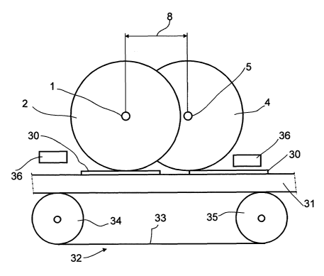
Figure 2 shows a side view of a device designed according to the invention.
Figure 2 shows the way in which the first disks 2 engage in the second disks
4.
The contact of the disks 2, 4 with the electrically conductive structures 30
to be
coated on the substrate 31 takes place with the spacing of the axial mid-
points of
the first shaft 1 and the second shaft 5. The closer together the axial mid-
points of
the first shaft 1 and the second shaft 5 lie, the closer together the contact
points of
the first disks 2 and the second disks 4 with the substrate lie. The spacing
with
which the first disks 2 and the second disks 4 touch the substrate is denoted
by
reference numeral 8.
In the embodiment represented here, the substrate 31 is transported through
the
bath of electrolyte solution by means of a transport device 32. The transport
device 32 in the embodiment represented here comprises an endless belt 33
which runs around two shafts 34, 35. The distance between the belt 33 and the
disks 2, 4 is selected so that the substrate 31 with the electrically
conductive
structures 30 is pressed onto the disks 2, 4 with a defined application force.
The
electrically conductive structures 30 may optionally be pressed onto the disks
2, 4
by mounting the transport device 32 fixed and, for example, pressing the disks
2,
4 with a predetermined application force onto the substrate 31 with the
electrically
conductive structures 30, to which end the shafts 1, 5 of the disks 2, 4 may
be
resiliently mounted. Alternatively, the axles 1, 5 of the disks 2, 4 may be
mounted
fixed and a predetermined application pressure may be exerted on the substrate
31 by the transport device 32. To this end, the shafts 34, 35 of the transport
device 32 are preferably mounted resiliently. Instead of a transport device 32
as
represented in Figure 2, a plurality of individual shafts arranged next to one
another may also be used as a transport device. Instead of the transport
device
32, it is also possible to provide a second device according to the invention
which
comprises at least two axles with inter-engaging disks arranged on them.
CA 02647969 2008-09-30 pF 0000057941/HMS
-16-
In order to ensure the transport, it is possible to drive either the axles 1,
5 on
which the disks 2, 4 are fastened or the shafts 34, 35 with the endless belt
33. It is
also possible to drive both the axles 1, 5 with the disks 2, 4 arranged on
them and
the shafts 34, 35. The drive of the shafts 1, 5 and 34, 35 is preferably
arranged
outside the bath. On the one harid each shaft 1, 5, 34, 35 may be driven
individually, although preferably the shafts 1 and 5 are driven by a first
drive and
the shafts 34 and 35 are driven by a second drive, or all the shafts 1, 5, 34,
35 are
driven by a common drive. The individual shafts 1, 5 and/or 34, 35, for
example,
connected together via gearwheels or chain or belt transmissions.
So that a current can flow in the electrolyte solution and electrolytic
coating of the
electrically conductive structures 30 is therefore made possible, anodes 36
are
furthermore provided in the bath. The anodes 36 may for example, as
represented
here, be configured in the form of flat rods. The anodes 36 are preferably
arranged in the vicinity of the electrically conductive structure 30 to be
coated. In
this case, care should be taken that the anodes 36 do not touch the
electrically
conductive structure 30 since otherwise the metal already deposited on it
would
be removed again. Besides the embodiment of the anodes 36 in the form of flat
rods, the anodes 36 may also be configured as flat metal or as elastic wires,
for
example spiral wires. It is also possible to use other anode forms known to
the
person skilled in the art. The anodes may be both insoluble and soluble.
The material for insoluble anodes 36 is known to the person skilled in the
art. For
soluble anodes 36, it is preferable to use the metal which is deposited on the
electrically conductive structures 30.
Figure 3 shows a side view of a device designed according to the invention in
a
further embodiment.
In contrast to the embodiment represented in Figure 2, with the device shown
in
Figure 3 it is possible to coat electrically conductive structures 30
simultaneously
on the upper side and the lower sicie of the substrate 31. It is also possible
to
electrolytically coat holes 37 in the substrate and thus obtain an
electrically
conductive connection between the electrically conductive structure 30 on the
upper side and the electrically conductive structure 30 on the lower side of
the
substrate 31. To this end, respectively, a device which comprises at least two
shafts 1, 5 with inter-engaging disks 2, 4 arranged on them is arranged on the
CA 02647969 2008-09-30 PF 0000057941/HMS
-17-
upper side of the substrate 31, and a device which comprises at least two
shafts
1, 5 with inter-engaging disks 2, 4 arranged on them is arranged on the lower
side
of the substrate 31. The substrate is guided through between the devices. The
substrate is preferably transported by the disks 2, 4, which contact the
electrically
conductive structures 30. To this end either all the shafts 1, 5 on which the
disks
2, 4 are arranged are driven, or only individual shafts 1, 5 are driven while
the
other shafts are mounted so that they are set in rotation by the substrate 31
when
the substrate is contacted by the disks 2, 4 on these shafts.
Figure 4 shows a shaft designed according to the invention with a disk mounted
on it.
A disk 10 as represented in Figure 4 comprises individual sections 11. The
sections 11 are respectively insulated electrically from one another by an
insulation 12. This, for example, makes it possible for sections 11 lying next
to one
another to be connected differently. For example, one section 11 may be
connected cathodically while the adjacent section 11 is connected anodically.
The
advantage of this embodiment is that metal which deposits on the section 11
while
it is connected cathodically is removed again from this section 11 when it is
connected anodically. This removal of the metal deposited on the individual
sections 11 is possible during operation of the coating device. So that
sections 11
lying next to one another can be connected differently, either its own current
supply 13 is provided separately for each section 11 on each individual disk
10 or,
since the neighboring sections 11 of disks 10 lying next to one another can
respectively be connected in the same way, a continuous current supply 13 is
provided with which the respectively adjacent sections 11 of the adjacent
disks 10
are contacted. An insulated cable which is fastened on the outer circumference
of
the rolls, for example, is suitable as the current supply 13. Instead of on
the outer
circumference of the shaft 14, the insulated cable may also extend inside the
shaft
14. To this end, for example, it is necessary for the shaft 14 to be designed
as a
hollow shaft.
Besides the current supply via an insulated cable, the current supply may also
take place directly via the shaft. To this end, for disks 10 which are
constructed in
individual sections 11 electrically insulated from one another, the shaft 14
is
likewise constructed in individual sections electrically insulated from one
another.
The current supply may then respectively take place via the individual
electrically
conductive sections of the shaft 14. To this end, the sections 11 of the disk
10 are
CA 02647969 2008-09-30 PF 0000057941/HMS
-18-
respectively connected to an electrically conductive section of the shaft 14.
When the current supply to the individual sections 11 of the disk 10
respectively
takes place via a current supply 13 in the form of an insulated cable, the
individual
sections 11 are for example respectively connected to the current supply 13 by
cable connections 15. The cable connection 15 may - as represented in Figure 4
-
be arranged on the outside of the disk 10, although it is also possible to
provide
the cable connections 15 on the end of the individual segments 11 facing the
shaft
14, in order avoid any lateral broadening of the disks 10. This may, for
example,
be done using a pin which is inserted into an insulated cable serving as the
current supply 13.
Figure 5 shows a side view of a disk according to Figure 4.
In the embodiment represented here, the current supply of the individual
segments 11 of the disk 10 takes place via individual insulated cables which
are
arranged on the outer circumference of the shaft 14. When a plurality of disks
10
are arranged next to one another ori the same shaft 14, openings through which
the cables 17 can be guided are preferably formed in the individual segments
11
on the side facing the shaft 14. The individual segments 11 are connected to
the
cable 14 via contact connections 15.
In order to improve the electrolyte supply to the substrate to be coated,
recesses
16 may be formed in the segments 11. In this case, the electrolyte solution
can
flow through the recesses 16. The recesses 16 may respectively be formed only
in
individual segments 11 of the disk 10 or in all segments 11 of the disk 10.
Furthermore, instead of the recesses 16 in the disk 10, it is also possible to
configure the disk 10 in the form of a wheel in which an electrically
conductive ring
with individual spokes is fitted on the shaft 14. In order to permit
electrolytic
coating of a substrate, it is necessary for the disk 10 to be electrically
conductive
on its outer circumference. To this end, for example, it is possible to
provide the
disk 10 with an annular contacting region 18 which is provided on the outer
circumference of the disk 10. The conventional material known to the person
skilled in the art, which is currently used for insoluble anodes, is for
example
suitable as a material for the annular contacting region 18. This may, for
example,
be titanium coated with a conductive rnixture of metal oxides.
When only the annular contacting region 18 is configured to be electrically
CA 02647969 2008-09-30 PF 0000057941/HMS
-19-
conductive, the individual segments 11 may be made of an electrically
insulating
material in the region between the annular contacting region 18 and the shaft
14.
In this case, it is merely necessary to provide a current conductor either
through
the electrically conductive material or on the surface of the individual
segments,
by which the voltage from the current supply 13, which in the embodiment
represented here is configured as cables 17 that rest on the outer
circumference
of the shaft, can be carried to the annular contacting region 18. When only
the
annular contacting region 18 is configured to be electrically conductive, in
order to
permit anodic and cathodic connection alternately it is sufficient for the
insulation
12 to be provided respectively between individual segments 19 of the annular
contacting region 18. Directly by means of this, the segments 19 of the
annular
contacting region 18 are electrically insulated from one another sufficiently
in
order to avoid a short circuit between an anodically connected segment 19 and
a
cathodically connected segment 19.
Figure 6 shows an embodiment of a current supply of a device designed
according to the invention.
The current supply to a shaft 14 with disks 10 arranged on it may, for
example,
take place via a further disk 20 arranged outside the bath of electrolyte
solution.
The further disk 20 is, for example, constructed like a disk 10 with which the
substrate to be coated is contacted. To this end, the further disk 20 likewise
comprises an annular contacting region 18 which is divided into individual
segments 19. Instead of an annular contacting region 18, it is also possible
for the
individual segments 11 of the further disk 20 to be respectively made entirely
of an
electrically conductive material. To reduce weight, it is possible to provide
recesses 16 in the individual segments 11 for the further disk 20 as well. The
recesses 16 may be formed in each segment 11 or only in individual segments
11.
The individual segments 19 of the annular contacting region 18 are
electrically
connected to the current supply 13 which, in the embodiment represented in
Figure 6, is likewise designed in the form of cables 17 that are arranged on
the
outer circumference of the shaft 14.
When the entire sections 11 are made of an electrically conductive material,
it is
preferable for the further disk 20 to be provided with an electrical
insulation on its
end faces so that there is an electrically conductive surface only on the
outer
circumference. This can prevent injury from occurring as a result of
inadvertently
touching the disk 20.
CA 02647969 2008-09-30
PF 0000057941/HMS
-20-
In order to supply the annular contacting region 18 with voltage, in the
embodiment represented here a cathodic sliding contact 21 which is connected
to
a cathodic current supply 22, and an anodic sliding contact 23 which is
connected
to an anodic current supply 24 arE: provided. Any sliding contact known to the
person skilled in the art may be used as an cathodic sliding contact 21 and as
an
anodic sliding contact 23.
When the shaft is constructed frorn individual electrically conductive
segments
which are separated from one another by an insulation, the current supply may
also take place directly to the shaft via sliding contacts. A further disk 20
is not
necessary in this case.
In order to avoid a short circuit, sufficiently large distances 25 should
respectively
be provided between the anodic sliding contact 23 and the cathodic sliding
contact
21. The distance 25 between the anodic sliding contact 23 and the cathodic
sliding contact 21 must be greater than the width of a segment 19. If the
width of a
section 25 is less than or equal to the width of a segment 19, a short circuit
will
take place each time the segment 19 simultaneously touches the cathodic
sliding
contact 21 and the anodic sliding coritact 23.
So that all the metal which deposits on the disks 10 while they are connected
cathodically can be removed from them again, the anodically contact region is
preferably larger than the cathodic contact region. This means that preferably
more segments are connected anodically than are connected cathodically. The
maximum number of cathodically connected segments 19 corresponds to the
number of anodically connected segrnents 19.
In the case of cables 17 extending radially on the shaft 14, with the
embodiment
represented in Figure 5 the substrate to be coated should be guided along the
lower side of the disks 10. If the substrate is to be guided along the upper
side of
the disks 10 so that the lower side of the substrate is coated, the cathodic
sliding
contact must be arranged on the upper side of the further disk 20 and the
anodic
sliding contact on the lower side of the further disk 20.
In order to be able to coat a substrate simultaneously on its upper side and
its
lower side, it is possible to arrange two electrolytic coating devices above
one
another or next to one another, the substrate being guided through between the
CA 02647969 2008-09-30
PF 0000057941/HMS
-21-
devices so that it is contacted simuli:aneously on its upper side and its
lower side
by the disks 10.
So long as the segments with which cathodic contacting of the substrate takes
place lie inside the electrolyte solution, the substrate can be guided along
the
individual devices at any desired angle. It is not necessary for the substrate
to be
transported through the bath horizontally, i.e. parallel to the liquid
surface. If the
substrate to be coated is held firmly enough, for example, it is even possible
for it
to be guided perpendicularly to the liquid surface along the disks 10 for
contacting.
CA 02647969 2008-09-30 pF 0000057941/HMS
-22-
List of References
1 first shaft
2 first disk
3 spacing of the first disks
4 second disk
5 second shaft
6 spacing of the second disks
7 engagement depth
8 spacing of the contact points
10 disk
11 section
12 insulation
13 current supply
14 shaft
15 cable connection
16 recess
17 cable
18 annular contacting region
19 segment
20 further disk
21 cathodic sliding contact
22 cathodic current supply
23 anodic sliding contact
24 anodic current supply
25 spacing
electrically conductive structure
31 substrate
30 32 transport device
33 endless belt
34 shafts
shafts
36 anode
35 37 hole in the substrate 31