Note: Descriptions are shown in the official language in which they were submitted.
CA 02648814 2008-10-09
WO 2007/115357 PCT/AU2007/000435
IMAGING APPARATUS WITH A PLURALITY OF SHUTTER ELEMENTS
CROSS REFERENCE TO RELATED APPLICATIONS
This application claims priority to US provisional patent application number
US
60/790,542, filed on 10 April 2006, the entire contents of which are
incorporated herein
by reference. This application also claims priority from Australian
provisional patent
application AU 2006901854, filed on 10 April 2006, the entire contents of
which are
incorporated herein by reference. This application also claims priority from
International (PCT) application PCT/IB2006/003311, filed on 22 November 2006,
the
entire contents of which are incorporated herein by reference. This
application also
claims priority from International (PCT) application PCT/AU2007/000012, filed
on 11
January 2007, the entire contents of which are incorporated herein by
reference. This
application also claims priority from International (PCT) application
PCT/AU2007/000061, filed on 24 January 2007, the entire contents of which are
incorporated herein by reference. This application also claims priority from
International (PCT) application PCT/AU2007/000062, filed on 24 January 2007,
the
entire contents of which are incorporated herein by reference.
FIELD OF THE INVENTION
This invention relates generally to systems and methods for modulating light
paths in association with shutter systems.
BACKGROUND OF THE INVENTION
Shutters are typically used in imaging, spectrometer and communication
designs to control light ingress to a sensor or sensor system. A common
example is in
the field of camera systems in which shutters are often used to manage the
amount of
exposure a sensor receives. Such shutters are often mechanicai in nature and
operate as a single shutter to attenuate all of the light from the entire
entrance/exit
aperture.
In camera systems complex optical lens and electronic signal processing
arrangements are often required, for example to correct aberrations, control
zoom, for
numerical aperture, to optimise exposure levels, and for speed of acquisition.
SUBSTITUTE SHEET (RULE 26) RO/AU
CA 02648814 2008-10-09
WO 2007/115357 PCT/AU2007/000435
Furthermore for a given camera system there is often a trade-off between
these, and
other parameters, that affect the quality of the acquired image.
Detection system resolution is typically affected by the density and size of
the
detector array. However, in many cases, this is, limited by manufactudng
capability
and fabrication costs. Another limitation in many colour detection systems is
that full
colour imaging is provided by the colour filtering associated with each pixel.
In most
cases this effectively reduces the number of imaging pixels, as 3 or 4
individually
coloureti pixels (red, blue, and one or two green) are required for each fully
coloured
image pixel.
Illumination and projection systems are often limited in their beam delivery
and
often don't have methods for dynamically attenuating parts of the beam.
Alteration of
beam delivery is useful in many applications for selective illuniination,
image control,
image compensation, and communications.
In fibre optic systems, electronic shutter arrays have been used in the past
to
switch signals between different waveguides. For example, as described in US
patent
5,185,824 in which an NxN array of stacked moulded splitter waveguides is
interfaced
to a matching array of combiner waveguides separated by an array of electronic
shutters.
In spectrometer systems, shutters have been used to control sample and
reference measurement, as well as enhance the waveiength-selective optics. US
patent 6,836,325 dcscribos an optical probo with an eleotrically activated
shutter
system to enable either an internal reference measurement or sample
illumination
while measurement is performed separately.
US Patent 4,193,691 describes the use of an LCD placed after the refractive or
diffractive element in a correlation spectrometer to form slits for specific
wavelength
detectian. Previously slits had been manually inserted into the spectrometer
according
to the spectral lines of interest. With the technique described in US
4,193,691, the slits
may be electronically configured and the signals may be modulated to allow
detection
from a sinrd. le pcint rlptPr,ter.
A similar system is described in US Patent 5,457,530 in which a Lead-
Lanthanum-Zirconate-Titanate (PIZT) optical shutter system is placed after a
diffractive element to diffract incident light according to wavelengths and
thereby
provide selective wavelength gating to a sensor. Each optical shutter element
is
applied with a voltage corresponding to the band of the ray incident upon the
optical
shutter element according to a specified timing so that the ray passes through
the
2
CA 02648814 2008-10-09
WO 2007/115357 PCT/AU2007/000435
optical shutter element.
US Patent 4,256,405 uses an LC.D shutter to pass light from different spatial
(ooations on a single sample through a lenr, and interfcrcncc filtcr that is
placed at an
angle to the optical axis to allow scanning of the spectraf pass band across a
detector.
This produces a spectral response of the sample from a single detector with no
moving
parts. This method images points of the sample at different parts of the
spectrum,
providing a single total spectrum that is representative of the sample as a
whole.
Consequently, this method assumes the spectrum is consistent across the imaged
sample and does not provide for spectral imaging at multiple spatial locations
on a
sample.
US Patent 6,191,860 provides a method for wavelength dependent detection by
switching a number of shutters that have predeterrnined wavelength attenuation
(or
filtering) optically associated with each shutter. According to the disclosure
in the
specification, this enables wavelength dependent detection.
The above mentioned spectrometer systems only enable spectral acquisition
from a single point sourcc. Typioaally in ~,ysterns in which more than one
sampla or
reference point is required, then dual or multiple spectrometers are often
used. Where
an area needs to be imaged by a spectrophotometer, as with Hyper-spectral
imaging,
then the optiCal input to a spectrometer is usually scanned across the sample
of
interest to build up a 3D data set (2 spatial and one spectral axis). An
alternative
approach is tu tdke urre full irriage recorded sequentially at each individual
wavelength.
These scanning systems are typically relatively large, fragile and expensive.
Improved methods for high resolution and multiplexed imaging of both spectral
and 2D data are reqi.rirwd fnr low cost and portable devices.
The reference to any prior art in this specification is not, and should not be
taken as, an acknowledgement or any form of suggestlon that the prlor art
forms part
of the common general knowledge.
SUMMARY OF THE INVENTfQN
In certain embodiments, the present invention provides apparatus and methods
for the control of electromagnetic waves through the use of one or more
shutter
elements. The electromagnetic wave, which may for example, be light, may be
controlled for a variety of purposes in areas including, but not limited to;
photography,
spectrosr.opy, microscopy, telescopy, imaging, illumination, image projection,
~
CA 02648814 2008-10-09
WO 2007/115357 PCT/AU2007/000435
calibration, and communications.
According to one aspect of the invention, there is provided an apparatus for
controlling the passage of an electromagnetic wave, comprising a shutter
operable to
control passage of an electromagnetic wave. In some embodiments, there are
provided a plurality of shutters each operable to control passage of an
electromagnetic
wave. The shutters may be arranged in any suitable fashion, for example, they
may
be arranged linearly, 2-dimensionally or 3-dimensionally.
An apparatus according to this aspect of the invention may be used for any
suitable purpose, for example, it may be used for one or more of analytical,
photography, spectroscopy, microscopy, telescopy, imaging, illumination,
communication, image projection, and / or calibration use.
In some embodiments, the apparatus is such that multiple samples and / or
references may be analysed simultaneously. Gertain embodiments may be more
suitable to particular areas of technology. In some preferred embodinients,
there is
provided an apparatus for use in microfluidics.
Control of the electromagnetic wave may be by any suitable means. For
example, it may be by controlling one or more of the timing, frequency, and /
or duty
cycle of the shutter elements. An apparatus according to the present invention
may
also be used in a variety of systems, for example, it may be used in one or
more of an
illumination system, detection system, and / or image projection system.
Control of tho olcctromagnotic wave by a shutter element may bring about any
suitable or required effect. For example, in some embodiments, the
electromagnetic
wave is controlled by the shutter elements to cause one or more of, altering
the beam,
blocking the beam. absorbing the beam, attenuate the beam, pattem the beam,
shape
the beam, refracting the beam, reflecting the beam, slowing the beam,
redirecting
some or all uf tfie buarn, fui example, through different pathways, and
homogenise the
beam or modulation of frequency, modulation of amplitude, modulation of,
timing, of the
electromagnetic wave.
SomP embodiments are particularly suited to calibrate an electromagnetic wave
and optionally oalibrate a light beam.
Some embodiments of the Inventlon may be suitable for use with a proximal
device. In some of these embodiments, information from the proximal device is
used
to alter operation of one or more shutters.
The invention also extends to proximal devices suitable for use with an
apparatus for controlling the passage of an electromagnetic wave according to
the
4
CA 02648814 2008-10-09
WO 2007/115357 PCT/AU2007/000435
pi-esent invention.
In some embodiments, the shutter element or elements are operable between
ot loast two states associated with electromagnetic wave control. Shutters and
/ or
shutter elements may comprise any suitable materials, for example, liquid
crystal,
optionally head-Lanthanum-Zirconate-Titanate (PLZT). Shutters and shutter
elements
may comprise any suitable other components, for example, a MEMS micromirror
device.
A shutter or 5hullei elemenl may be configured in any suitab(e way. For
example, it may be capable of corresponding to one or more pixels in an
associated
image.
fn a second aspect of the invention. there is provided a controller to control
at
least one shutter or shutter element. According to some embodiments, the
shutter
elements may operate independently, dependently, In a coordinated fashion,
individually or in a group to control the passage of electronic radiation.
] 5 The controller and shutter or shutter elements may interact in any
suitable way_
Thus, in some embodiments, the controNer controls the shutter which controls
the
electromagnetic wave by fully or partially causing one or more of blocking,
absorption,
alteration, filtering, splitting, attenuation, redirection, reflection,
refraction, slowing,
shaping, patterning, homogenising, modulation of frequency, modulation of
amplitude,
modulation of timing, of the electromagnetic wave. The controller may control
any
suitable aspect, for exampfe the controller may be operable to control one or
more of
timing, frequency, duty cycle, or sequence of operation of the shutters. The
controller
may also be operable to provide spatial information to a detection system.
This may
be irrespective of the number of detection elements in the detection system.
In some embodiments, the controller comprises a feedback mechanism to allow
a change in control of one or more shutters in response to feedt,dak. Ttie
cvntroNer
may also comprise a sensor, for example, to sense information on which the
feedback
is based.
In some ombc+diments, the controllPr may b? npprahlp to modulate multiple
electromagnetic wave sources to distinguish their origin, and / or to
distinguish
emissions caused by the excitation of one or more modulated sources, rn some
embodiments, the controller may be adapted for use with a proximal device and
information from the proximal device may be used to alter operation of one or
more
shuttGrs.
In some embodiments of the apparatus according to the present invention, there
5
CA 02648814 2008-10-09
WO 2007/115357 PCT/AU2007/000435
is further provided an an electromagnetic wave source. The source may in some
embodiments comprise a plurality of sources which are optionally coordinated
amongst
t hcrosclvos and / or with thc controller and / or one or more shutters.
In another aspect of the invention, there is provided an electromagnetic wave
source for use with an apparatus according to the invention.
In another aspect of the invention, there is provided an apparatus for
controlling
the passage of an electromagnetic wave and further comprising an
electromagnetic
wave detector.
In another aspect of the invention, there is provided a detector for an
apparatus
for controlling the passage of an electromagnetic wave. The detector may take
any
suitable form and comprise any suitable furthpr r..ompnnwnts, fnr pxample, it
may
comprise an array of detector elements, it may comprise a micro-lens array. In
some
embodiments, each detector element is operable to a plura-ity of
electromagnetlc
beams or waves either together, or separately (for example, in separate
frames), and
in some embodiments, the entire imaged area may be detected.
In some embodiments of this aspect of the invention, the detector is operable
to
distinguish an electromagnetic wave that has interacted with at least one
shutter. The
elect roniag netic wave may be distinguished based on any suitable
characteristics, for
example, time and I or frequency domain techniques, information received from
a
shutter system and optionally a controller, on shutter timing, attenuation of
a signal
using a signal processing technique.
A detector according to the present invention may comprise any suitable
detection device, component or equipment, for example, it may comprise one or
more
of a spectrometer, charged coupled device (CCD), photodiode (PD), avalanche
photodiode (APD), phototransistor, photo-multiplier tube (PMT), complimentary
metal-
oxide semiconductor (CMOS) sensors, charge-injection device (CID).
In another aspect of the invention, there is provided for an apparatus for
controlling the passage of an electromagnetic wave and further comprising an
image
reconstructor to reconstruct a signal associated with an electrom2gnotir..
wave
previously the subject of control according to the present invention.
In another aspect of the invention, there is provided an image reconstructor
for
an for an apparatus for controlling the passage of an electromagnetic wave.
The
image reconstructor may be operable to reconstruct an image based on
information
from any suitable source, for oxomplo ono or more of: electromagnetic wave
gourca(s),
shutter(s), detector(s), and / or controller(s). The image reconstructot may
reconstruct
6
CA 02648814 2008-10-09
WO 2007/115357 PCT/AU2007/000435
an image based on coordination of information, for example, coordination of
one or
more of: electromagnetic wave source(s), shutter(s), detector(s), and / or
pontroller(s)_
In some embodiments, the image reconstructor may be operable to reconstruct
an image based on one or more of time domain and / or frequency dornafn, a
signal
analysis method which may optionally be Fourier Transform Analysis. Images may
be
reconstructed by reconstructing electromagnetic waves optionally individually,
or in
one or more groups_
In some enibotliments of the invention, greater image.control is achieved by
one
or more of signal levelling and 1 or calibration factors. The calibration
factors may be
applied to specified spatial locations, and optionally by attenuating one or
more
sign2ls: In Gnmp Pmhnrlimt?nt:s, the atrparatus of the invention is operable
to increase
the signal to noise response and optionally by using one or more of timing and
or
frequency analysis teChniques. In some embodiments, tne apparatus of the
Invention
is operable to achieve greater wavelength separation and resolution and
optionally
with one or more of timing and or frequency analysis techniques.
In some embodiments, mu-tiplexod inputs from a plurality of shutters inc:rease
the throughput and / or imaging capabilities of the system and optionally
without the
use of moving parts, or optionally without the use of complex moving parts.
In some embodiments, multiplexed inputs from a plurality of shutters increase
the throughput and / or imaging capabilities of the system and optionally
without the
use of complex moving parts. Furthermore, the apparatus may be operable to
acquirc
data from a plurality of spatial locations and optionally all spatial
locations and
optionally by shutter modulation. The apparatus may also be operable to
simultaneously or sequentially allow one or more components of an imaqe past
one or
niore shutters. (n some embodiments, a plurality of shutters each sequentially
allow a
component of an image to travel past drrd thereby fdll ir7cider7t un a
detector.
A wide variety of image improvement techniques may be employed using the
apparatus of the present invention. Thus. for example, there may be one or
more of
dynamic image .r.nntrr)l, fePrihar.k mer.hanisms, reshaping, redirecting,
image overlap
techniques. In some embodiments, the apparatus is operable to provide
simultaneous
signal measurement from separate spatial locations optionally with shutter
timing and /
or frequency modulation. Image resolution may also be improved by imaging more
than one pixel, or group of pixels of from a shuttering system onto one or
more of the
uamo pixal~ of a dctector. In some embodiments, ths apparatus is operable to
multiplex light paths onto the same detector or optionally, a group of
detector
7
CA 02648814 2008-10-09
WO 2007/115357 PCT/AU2007/000435
elements.
In some embodiments, the apparatus is operable to decrease aberrations.
Thus, for example, the same image is overlain through different paths and
aberrations
reduced by a digital signal processing technique. Furthermore, an apparatus
according to the present invention may be operable to achieve one or more of
increased depth of field, improved zoominq, focal depth enhancement, 3-
dimensional
imaging, panorama imaging and / or multi-image processing. The apparatus may
also
he opeiable to image a plurality perspectives of an object through a plurality
of lens
systems via at least one shutter or shutter element and onto a single
detector. In
addition, the apparatus may be operable to multiplex light paths onto separate
detectors or detector elements and optionally to improve dynamic range and /
or
sensitivity.
The same image or portion of an image may be (ocused on more than one
detector element optionally to alter the sensitivity and / or dynamic range of
a detector
element. Furthermore, higher and lower sensitivity pixels may be created which
may
ertablo optionally high and / or low contrast images that may optionally be
digitally
processed to provide a further improved exposure image. In some embodiments,
an
incident electromagnetic wave is attenuated by one or more shuttering elements
onto
the same detector or optionally group of detector elements to improve one or
more of
the sensitivity and / or dynamic range. In some embodiments, signal processing
to
measure the incident electromagnctic wavo prior to attcnuation ond thcreby
minimise
saturation of individual pixels.
A control system may be used to dynamically modify exposure of each detector
or group of detector elements and optionally in response to information about
the
incident electromagnetic wave. The information may be any suitable type and of
any
sultable form. For example, it may relate to any suitable characterislic of
ltte wave, (or
example intensity. The apparatus of the current invention may also be used to
control
aperture. In some embodiments, attenuation by one or more shutter elements or
shutters reduces the 2perture to an innidpnt alPctrnmagnetic wave.
The apparatus may comprise a filter and or separator which optionally filters
or
separates based on frequency or wavelength. The apparatus may also comprlse a
separator to separate an electromagnetic wave. The filter or separator may be
of any
suitable types, for example, it or they may comprise a colour filter or colour
separator.
In some embodiments, the apparatus is operable to filter or separate red,
green and
blue light. Futhermore, the apparatus may comprise a light separator to
separate red,
8
CA 02648814 2008-10-09
WO 2007/115357 PCT/AU2007/000435
green and blue light and wherein the separated light from one or more
individual
lenses per colour is detected by a single detector_
The eolours incident on a detector according to the present invention may be
from a single previously separated beam. The apparatus may be operable to
perfor-m
hyperspectral imaging. The apparatus may further comprise one or more of an
electromagnetic wave source, a detector. and / or an electromagnetic wave
director.
In some embodiments comprising a director, it is operable to direct, madify or
control
an electromagnetic wave. The director may clirect any required aspect of a
wave, ror
example, it may be operable to focus and / or shape an electromagnetic wave.
In
some embodiments, the apparatus is operable to focus an incident wave on a
particular area of a detector and / or selectively detect a wave arising frorn
a particul2r
area. In some embodiments, the director is operable to perform one or more of
focusing, redirecting, slowing, attenuating, pulsing, separating, filtering,
or otherwise
altering an electromagnetic wave. A director according to the present
invention may
further comprise a shutter or shutter element as herein described.
The apparatus may further comprise one or more of a wavoguido, lens,
microlens array, collimator, mirror, micro mirror, filter element, polarizer,
prism, grating,
fiber optic element, each of which may take any suitable form. For example, in
some
embodiments, the apparatus comprises an optical fibre element operable to
interface
with one or more of a source, detector and / or controller_ The optical fibre
element
may eornprise a burictle uf optical fibres and at least one shutter controls
the passage
of an electromagnetic wave entering or exiting from the optical fibre efement.
The apparatus of the present invention may be operable to interface with a
proximal device which is optionally a microfluidics device_ The apparatus of
the
present invention may further comprise a filter in the electromagnetic wave
path and
wherein the filter optionally compnses one or more of absorptive, reflective
and / or
liquid crystal tuneable elements. The filter may take any suitable form and be
placed
at any suitable Iocation. For example, the filter may be physically one or
more of
intogrotod into an optical bench, integrated with a micro{luidics device,
associated with
at least one shutter or removable_
In another aspect of the present invention, there is provided an optical bench
for
use with a shutter or shutter element and / or apparatus according to the
present
invention. The optical bench may itself be for use with a proximal device,
which may
optionally be a microfluidics device. The optical bench may optionally
compriss one or
more of a broad band light source and a laser source and / or at least one
light altering
9
CA 02648814 2008-10-09
WO 2007/115357 PCT/AU2007/000435
component which is optionally a filter, a director, and / or a separator. In
some
embodiments, the proximal device may comprise a light altering component. In
some
embodiments, one or more shutter elements are associated with the beam path
from
the light altering components.
The optical bench may further comprise a light source which is optionally a
plurality of Laser sources, and optionally further cornprising one or more
beam
expanders, and shutter elements. Furthermore, beams from more than one source,
or
light having passed through more lharr urre fiyht alleriny componertt, riiay
illuminate an
overlapping area. In some embodiments, the optical bench may comprise a
detection
shutter. In some embodirnents the proximal device may be for use with a
proximal
device wherein informatinn from the proximal dFvir¾ is risPCi to alter
r,pPration of one
or more shutters. A proximal device for use with such an optical bench is also
contemplated by the present invention.
DESCRIPTION OF DRAWINGS
Figures 1A-D are diagrammatic illustrations of shutter elements according to
one aspect of the invention which are passing, stopping and reflecting light.
Figures 2A-E are diagrarnmatic illustrations of shutter elements which are
passing, stopping, reflecting and extending light paths.
Figures 3A-G depict images associated with shutter systems in whioh shutter
elements may be operated with different timing and frequency characteristics.
Figure 4 is a flow diagram illustrating separate image acquisition through
shuttered element processing and combining into an optimised image.
Figures 5 is a flow diagram illustrating simultaneous image acquisition
through
shuttered elements with a separate image processing priur tu cumtJining far an
optimised image.
Figures 6A-C are diagrammatic illustrations of the use of control systems to
operate the shutter systems with feedback from sensor devices.
Figures 7A-13 depict images demonstrating the use of shutter elements to
homogenise and pattern a oross section of a light path.
Figures 8A-C depict optical and shutter elements interfaced to three different
sensor surfaces.
Figure 9 dcpicts on optieol imaging system with a Ehutter array component and
single detector or source element.
CA 02648814 2008-10-09
WO 2007/115357 PCT/AU2007/000435
Figure 10 depicts an optical imaging system with a shutter array component and
detector with multiple detection elements.
Figure 11 depicts an example of an optical imaging system using a shutter
array
with a micro-lens array to image each shuttered element onto a detector array.
Figure 12 depicts an example of an optical imaging system in which the light
passing through every shutter element, or group of shutter elements, images an
object
onto the entire sensor surface.
Figure 13 depicts an example of an optical imaging systeni in which the light
passing through every shutter element, or groups of shutter elements, images
an area
at different focal depths, or perspectives, onto the entire sensor surface.
Figure 14 depicts an example of an optical system in which colour filtering
elements are associated with shutter and lens elements for imaging onto a
sensor
surface.
Figure 15 illustrates an example of an optical system in which three separate
lens elements image an object onto the same sensor surface through a
shuttering
system.
Figure 16 illustrates an example of an optical system in which an image is
acquired and split into three beams to pass through three separate shuttering
elements
and filters before recombining for imaging onto the same sensor.
Figure 17 illustrates examples of waveguides interfaced to shuttering systems
and source, or detector, devices,
Figure 18 illustrates an example of a shutter array interfaced to a fibre
optic
bundle.
Figures 19A-B illustrate examples of shuttering systems interfaced to
waveguides for detection or illumination on proximal devices.
Figures 20A-B illustrate liyfit pattis pdssing tfirough shuttering systems for
luminescent particle illumination or detection.
Figure 21 shows a wavelength versus intensity graph illustrating the combined
intpnsity from twn sPparatP snurr.PS_
Figure 22 depicts a side diagrammatic view of an example optical bench using a
shuttering system.
Figure 23 illustrates a top view of some components from an optical bench
according to one aspect of the present invention,
DETAILED DESCRIPTION OF THE DRAWINGS
11
CA 02648814 2008-10-09
WO 2007/115357 PCT/AU2007/000435
The following descriptions are specific embodiments of the present invention.
It
should be appreciated that these embodiments are described for purposes of
iliuetration only, and that numorous altorations and modifications may be
practiced by
those skilled in the art without departing from the spirit and scope of the
invention. For
example, the following description uses light as an example of electromagnetic
radiation, It is intended that all such modifications and alterations be
included insofar
as they come within the scope of the invention as claimed or the equivalents
thereof.
As used herein, the term "fluid" refers to either gases or liquids. As used
herein,
the term "microfluidic" refers to fluid handling, manipulation, or processing
carried out
in structures with at least one dimension less than one millimetre. As used
herein, the
term "light ray" refers to more than one photon travplling in a siihstantially
similar
direction.
Examples of advantages ot the current invention inclUde:
a. Selective illumination or detection of specific spatial locations, which
can
be simply provided by selectively opening and/ or closing shutter
clemcnts.
b. Control of multiple shutter elements may provide spatial information to a
detection system irrespective of how many detection elements the sensor
system has. This enables the spatial location of a sample or image to be
determined.
c. The ability to isolate different shutter locations for imaging and or
illumination_ This enables flexible spatial control for measurement or
illumination at multiple spatial locations. This invention provides greater
flPxihility and tolerances as the optical pathway can be adjusted to
accommodate the areas or structures to be imaged, analysed,
illuminated etc on the same or different proxlmal devices.
d. When shutter elements are combined with individual lens components
that image the shutter elements area over one or more element of the
same sensor, then there is effectively an increase in the resolution of the
sensor by a multiple of the number of imaged shutter elements operated
over the same sensor area.
e. Detection and source systems can be simplified by providing multiplexed
inputs from the shuttered elements, increasing the throughput and
imaging capabilities of the system without thc usc of moving parts. This
may be important in various situations, for example in hyper-spectral
1=2
CA 02648814 2008-10-09
WO 2007/115357 PCT/AU2007/000435
imaging, which may be performed with a single channel spectrometer
interfaced to a waveguide with a shutter array.
f. Fastor roading and processing of information. For example, whan
interfaced to spectrometer or camera systems the simultaneous
acquisition of spectral or image data from multiple spatial locations can
be provided by shutter timing and or frequency.
g. Simultaneous signal measurement from separate spatial locations with
shutter timing and or frequertcy niudulatiun. This ritay foi' example be
important for imaging and analysing non stationary or continuous
processes, such as moving samples or monitoring, processes, such as by
monitnrinrd rpaction kinPtirs,
h. Signal levelling and the application of calibration factors to specified
spatial locations can be performed by attenuation of the light rays
passing through the switching shutter elements. This may for example be
important for compensating for losses in the source or sensor optics that
may vary spatially and or over time, and for compensating for the
different rnaterials and path lengths used in proximal devices.
i. By imaging the same area onto the same sensor through different lens
and shutter elements, improvements can be gained through lens
aberration correction, focal depth enhancement, zooming, 3-dimensional
imaging, panorama, and oversized imaging. This provides particular
advantages, for example in camera system design and usage by allowing
a cheaper optical and electronic system design using the same sensor
system. This avoids camera repositioning or refocusing during use and
enables the same time and or positional reference to be used for multiple
images. Consequently, simultaneous image acquisition for reai tirrie
perspective measurement is provided.
j. Increased dynamic range and sensitivity of detection systems by
providing gain control by light attenuation throtrgh thp shutfPring
elements on different parts of the light beam or image,
k. The modulation of a shutter array on the detector and or source optics
can increase the signal to noise response with the use of timing and or
frequency analysis techniques. This can be applied to spectroscopic
GyGtems for wavolongth soparation or imaging Eystems for improved
sensitivity and dynamic range.
13
CA 02648814 2008-10-09
WO 2007/115357 PCT/AU2007/000435
I. The shuttering elements can be used to dynamically alter the light
attenuation and modify the image.
According to one embodiment, the present invention comprises a device
comprising a shutter system with a plurality of elements. The shutter elements
may be
arranged in any suitable manner, for example, a 3-dimensional, 2-dimensional,
linear
array, nr he arrangPri as discrete shutter elements, or groups of shuttering
elements,
forming a shuttering system. The shutter elements may block, absorb, or
redirect light
and may be operable between at least two states. For example the shutter
elements
may be partially or wholly light absorbing or retlective. Figures 1A and 1B
show a three
element (101,102,103) light absorbing shutter, in Figure IA the elements block
the
passage of light (104) from a source (105) to a detector (106), and in Figure
113 the
middle element (102) is switched into a position to allow partial or complete
light
passage. Figures 1C and 1D illustrate an example of a three element
(107,108,109)
reflective shutter, in Figure 1C the shutter elements (107,108,109) are
aligned to
reflect the light (t 10) from the source (111) away from the detector (112),
and in Figure
1 D the middle reflective shutter (108) is aligned to reflect the light (113)
from the
source (111) to the detector (112).
Shutter elements may for example be placed in-line with an optical pathway and
act to attenuate the passage of light, or the shutter elements may be used to
redirect
the optical path and used to attenuate the light. Optical pathway redirection
is
important for example In systems In whlch the source and detector optics are
un lhe
same side and or where the optical pathway requires redirection through a
proximal
device. Optical pathway redirection is also important for example in systems
for
Absorption/Transmission sample measurements where tha light ray path r.an be
extended through the sample to improve the potential absorption within the
sample,
and where multiple areas need to be illuminated/detected in the same optica-
path.
Figure 2 ilfustrates examples of optical path changes to stop, pass and
reflect
the optical pathway. Figure ZA shows a configuration of a shutter in open
(201) and
olosed (202) position3 stopping (203) or pawing (204) light rays (200). Figure
28 and
C illustrate passing (205) or reflecting (206) light rays that are incident
either
perpendicular to or at an angle to the shutter array. Figure 2D represents an
example
of increasing the optical path length by reflecting a light ray between
multiple shutter
elements. Such an embodiment is useful for example for increasing the optical
path
length through a prQxinial device (207) placed in between the shutter arrays,
as shown
in Figure 2E.
14
CA 02648814 2008-10-09
WO 2007/115357 PCT/AU2007/000435
The shutter array controls the passage of light to the detector, or from a
source,
and each element within the shuttering system and may be operated
independently
from, or dependently with, other elements or groups of elements within the
array or
shuttering system. By modulating or tiniing the opening and or closing of some
or all of
the shutfering elements the light passing through the individual shutter
elements is
attPnuaterl in ar.r.ordance with that individual shutter's timing. For
example' a shutter
may be opened and closed once for a period of time, or the shutter element may
be
opened and closed more than once, and may be done at a particular frequency
and
duty cycle. The detection system may then reconstruct which light rays have
passed
through each particular shuttering element based upon the shutter's timing,
frequency
and or amplitude characteristics. Signal reconstruction methods can be based
on
shutter timing, for example, by time domain or frequency domain methods, such
as
Fourier transforms analysis, and or other signal analysis techniques.
For example in certain preferred embodiments the shuttering system includes a
2-dimensional shutter array. Figure 3A illustrates a 2-dimensional shutter
array (301)
in which only one element (302), or pixel, of the shutter array is opened at
any one
time. Alternatively, for example, the pixels within the shuttering array (301)
may be
modulated open and closed at different frequencies and or with different
timing either
individually or in groups. Figure 3B illustrates an example in which a group
of pixels
(303) are modulated at the same or different timings or frequencles. Figure 3C
Illustrates an example In which two separate groups of pixels (304,305) are
itioQulated
independently. Figure 3D illustrates an example in which two separate groups
of'pixels
(306,307) are modulated independently but each pixel within each pixet group
are
modulated together. Figure 3E illustrates an example of groups of pixpls
(308,309,310,311) modulated together that are not immediately adjacent to one
another. Figure 3F illustrates an example of a pixel array (301) where all tne
pixels are
operated independently from one another at different timing and or frequency
intervals.
In another preferred embodiment, as illustrated in Figure 3G, the shutter
array includes
individual shutter elements (313,314) or groups of shutter elements (312) that
form
separate shuttering elements within a shuttering system.
According to one embodiment of the invention a detection system can
distinguish light that has passed through, or been redirected by, separate
shutters or
groups of shutters by the attenuation of the light by the shutter system. Time
and or
frequenr:y dotliaili teGhniques can be used to separate the signals from one
another.
According to another embodiment of the invention a detection system can
CA 02648814 2008-10-09
WO 2007/115357 PCT/AU2007/000435
distinguish light that has passed through, or been redirected by, separate
shutters or
groups of shutters by either control over the shuttering system, using the
shutter timing
if known, or interpreting the results from the attenuation of the signal by
signal
processing techniques.
The reconstruction of the light rays passing through, or redireoted by, the
shutter elements may be achieved either individually, or in groups where the
timing is
the same; or it may be performed simultaneously with one or more of the other
shutter
elements or groups of 5huller elernenls. For exaitiple Figure 4 illustrates
the separate
acquisition of 3 images (401,402,403) from the same shutter array but with
different
shutter elements activated (404,405,406). The acquired images are processed
sPparately before recombining to form an optimised combined image.
Alternatively the
light passing through more than one shutter element may be acquired
simultaneously,
as per Figure 5, wnere a 2 dimenslonal array (501) has all of its shutter
elerrierils
modulated in one of three ways so that the light passing through these three
types of
shuttering element may be reconstructed as three separate signals or images.
In both
the examples of Figures 4 and 5 the signals are recombined after separate
processing
to form a single optimised image. This is particularly useful when the light
passing
through more than one shutter element is multiplexed to one or more sensor
elements.
In another embodiment feedback and control systems are used to operate the
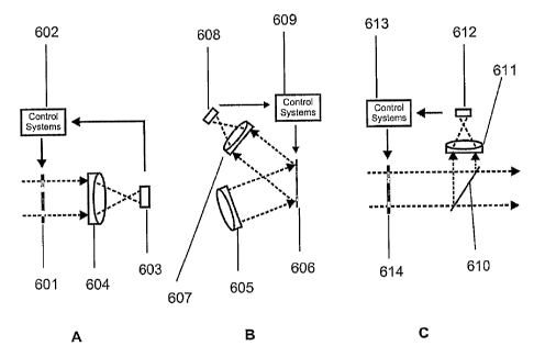
shutter system. In Figure 6A the shuttering system (601) is controlled by a
control
system (602) via feedbaok from an inline sensor (603) on which tho shuttered
light
from the lens system (604) is focused. In the example of Figure 6B the light
path from
the lens (605) is reflected from the shuttering system (606) that controls the
light path
redirection (attenuation) through the lens element (607) and onto the sensor
(608),
from which feedback control of the shuttering systems is provided through the
control system (609). The example of Figure 6C shows a partially reflective
mirror (610)
imaging the beam through the lens (611) onto an off-axis sensor element (612)
providing feedback to the controller (613) for controlling the shuttering
system (614).
This type of off-axis control arrangpmpnt is partir-,ularly suitable for
projection imaging
and illumination systems. In an altemative embodiment the shuttering system
may
contain internal sensor elements associated with one or more shuttering
elements,
thereby providing localised sensing for sensing and or control of the
shuttered
elements.
According to another embodimont the shuttering elements can be used to alter
light attenuation and provide image modification. This can be in the form of
displaying
16
CA 02648814 2008-10-09
WO 2007/115357 PCT/AU2007/000435
a secondary image overlaying the original image, or reshaping the existing
image, and
when combined with sensory feedback a controller system can provide feature
detection and objcct rccognition to provide dynamic image control.
tn another embodiment the attenuation of light by the shutter elements may
also
be used for communication. This includes the attenuation of optical
communication
signals by the shuttering system for qating, wavelenqth, or polarisation
alteration,
where such elements (optical filters and or polarisers) are associated with
the
shuttering elements, and rnullit,lexing lhe signals onto the same optical
path, or
aEternatively de-multiplexing signals from a plurality of optical paths. In
another
embodiment, the attenuation of the light by the shuttering elements may be
used to
provide the comrnUmiC8tinn signal by moctulating the light passing through the
shutter
elements which can provide timing, frequency, and or amplitude modulation of
the
light.
According to another embodiment the shutter system may be used as part of an
illumination system to attenuate the illumination beam. For gain control of
the entire
light be3m or parts of the light beam for providing either a patterned or
shaped beam,
redirecting parts of the beam onto different optical paths, or homogenising
the beam.
For example, Figure 7A illustrates the homogenising of a cross section of a
light beam
(701) by the shutter array (702), which is arranged so as to attenuate the
beam in
proportion with the beam intensity at each pixel, such that the beam (701)
after
passing through the shutter array (702) is uniform (703). In another exampic
tho boom
is patterned, as shown in Figure 7B. Attenuation of the beam (704) by the
shutter
array (705) is provided to only allow illumination through designated pixels
(706), which
results in the illumination pattern of (707). If light passing through the
separate
shuttering elements, or groups of shuttering elements, is combined with other
optical
elements suGh as lenses or fibre optics then lhe sfhutterirry elemerits can
provide
controlled light path redirection through these optical elements,
Light-directing elements may be used in conjunction with the shuttering
system,
such as fuil or partial reflective surfar_es, mirrors, micrnmirrnrs, gratings,
lenses.
microlenses, prisms, fibre optics, waveguides or other light-directing
devices, which
may be made from any suitable materials, tor example, silicon, glass, quartz,
polymers, metals, or composite materials_ The light-directing devices may
contain one
or more shuttering devices. Multiple light directing elements may be used.
According to
certFain profcrrod ombodiments, the shuttering device is an array and may be
an
electronic device such as a liquid crystal or PLZT device, MEMs micromirror
device, or
17
CA 02648814 2008-10-09
WO 2007/115357 PCT/AU2007/000435
other shuttering devices.
In general, light-directing devices can be used in the light ray path prior to
the
shuttering system tu foous IiyIiL onlo or through the shuttering eien-rents,
and or the
light-directing elements can be used to focus or guide light emitted from the
shuttering
elements. Light directing elements can be associated with guiding light to or
from;
individual shuttering elements to individual sensor or illurninatinn eIPments;
individual
shuttering elements to multiple sensor or illumination elements; multiple
shutter
elements to individual sensor or illumination elements. I hese three
respective cases
are illustrated in Figures BA, 8B, and 80 with the simple example of a
microlense array
(801) imaging through a shutter array (802) onto the sensor surfaces
(803,804,805).
According to one ombodimont of this invention, the shuttering element is
interfaced to a light-directing device to allow selective illumination of, or
detection from,
an object for imaging. An example of this is illustrated in Figure 9 in which
an optical
system is shown for imaqing an object (905) with a single detector (901)
through lens
systems (902, 904) having a shutter array (903). By modulating the shutters
open and
closed in lhe lirrre or frequency domains a 2-dimensional (2D) image can be
reconstructed from a single sensor by separating out the signals passing
through each
of the shutter elements or groups of shuttering elements, and then recombining
them
as a whnla image.
In another embodiment of the invention the resolution of a sensor array is
rmproved by imaging each pixel, or group o1' plxels, of the shutter onto more
thari une
pixel of the sensor array. An example of this is illustrated in Figure 10 in
which an
optical system is shown for imaging an object (1005) with a detector array
(1001)
through a Ions systom (1002,1004) having a shutter array (1003).
In a similar example Figure 11 illustrates an object (1105) imaged by a lens
system (1104) onto a micro lens (1102) and shutter (1003) array which images
each
micro-lens onto the entire sensor array (1101). In both these examples each
element,
or group of elements, of the sensor array may be used to effectively detect
the entire
imaged area from one or more shuttered clomonts. This can effectively incrAase
the
sensor resolution by the number of shuttered elements that are imaged over the
same
sensor area, i.e. 1 mega pixel CCD interfaced to a shuttered micro-lens array
of 100
where each micro lens is imaged over the entire sensor surface would have a
possible
resolution of lMxlOO = 100 mega pixels.
In anpttier ernbuifirnertt Lhe shuttering system can be used to multiplex
light
paths onto the same sensor (or group of sensor elements) for aberration
correction. By
18
CA 02648814 2008-10-09
WO 2007/115357 PCT/AU2007/000435
overlaying the same image through different optical paths, the deficiencies
and
aberrations induced from each of the separate optical paths can be reduced by
digital
signal processing techniques. The example of Figure 12 illustrates the
simplified case
of using lens arrays (1202, 1204) that image the same object (1205) onto the
same
sensor surface (1201) through the shuttering elements (1203), which can
attenuate the
separatp light paths for signal separation.
In another embodiment the shuttenng system can be used to multiplex light
paths onto separate sensors or attenuate the light passing througn to a sensor
element
(or group of sensor elements) for improved dynamic range & sensitivity. Where
the
same image or portion of an image is focused on more than one sensor element
then
the light may be attenuated through more than one shutter to effectively alter
the
sensitivity and dynamic range of the different sensor elements. This
consequently
provides higher and lower sensitivity pixels that can be used to create low
and high
contrast images that may be digitally processed to provide an optimum exposure
115 image. Similarly the sensitivity and dynamic range of a sensor element may
be
improved by attenuating the incident light through one or more shuttcring
olomonts
onto the same sensor, or group of sensor, elements. When the degree of
attenuation is
known, then signal processing can provide an accurate measure of the incident
light
prior to attenuation, and saturation of individual pixels can be avoided.
Where a control
system operates the shutter elements based on the intensity of the incident
light then
the shuttering elements may be cUrilrulleri dynamical(y allowing optimum
exposure of
each sensor element or group of sensor elements.
In another embodiment the shuttering system can be used to multiplex light
paths onto the same sensor for increased depth of field, 7nnming, and 3-
dimensional
imaging applications. In the example of Figure 13 a shuttering element is
disposed
between two l'ens systems (1;302, 13U4) that irnage the imaging zone (1305) at
different depths onto the sensor device (1301). By imaging an object multiple
times at
different focal lengths through a shuttering system (1303) onto the same
sensor then
either individuol imagos with different focal points can be produced, thereby
providing
a zoom effect, or the images can be digitalfy combined to provide a single
image with a
greater depth of field.
In another embodiment the shuttering system can be used to multiplex light
paths onto the same sensor for multi image processing and capture. By imaging
different objectives or perspectives of the same object through different
lensing
systems onto the same sensor through shuttering elements, the capture of
multiple
19
CA 02648814 2008-10-09
WO 2007/115357 PCT/AU2007/000435
images can be performed with the same sensor system.
In another embodiment the shuttering system can be used for aperture control.
Where the light passing through multiple shuttering elements is imaged onto a
sensor
surface, then some of the shuttering elements may be attenuated to reduce the
aperture of the incident light.
In annthpr Pmbodiment filtering components are associated with one or more
shuttedng elements and imaged onto a sensor surface using a lens system. In
the
exampie of Figure 14, tiltering components (1403) are associated with one or
more
shuttering elements (1402) and the image (1406) is projected through the micro-
lens
JO array (1404) by the lens system (1405) onto the sensor (1401) surface. Full
colour
imaging can be achieved through the modulation of the shutters controlling the
colour
attenuation. Thus, for example, there may be provided red, green and blue
(RGB)
filters arranged on each shutter element in a similar manner to groups A, B,
and C; in
Figures 4 and 5, and then every block of four RGB filters may be imaged onto
the
same pixel.
In another embodiment, discrete shutters are combinod with filtering
components such as RGB (red, green, blue) or color filters for color imaging
onto a
sensor surface. In the example of Figure 15 the 3 separate light paths,
imaging the
same object (15011) through the lens systems (1508,1509,1510) are combined
after
passing through the shuttered elements (1507a, 1507b,1507c) with there
respective
colour filters, red (1504), greeri (1505) ania blue (1506). The three beams
are then
combined through the reflective mirrors (1503a,1503b,1503c,1503d) and imaged
onto
the sensor (1501) surface through the lens system (1502). In another
embodiment a
single light path is split, filtered 2nd rwr..nmhinPd. ThP example of Figure
16 depicts a
single imaging lens system (1609) where the image of the object (1610) split
into 3
separate beams by the mirrors (1608a,16Udb,16U6c,1608d) before passing through
three separate shutters (1607a,1607b,1607c) with filter elements
(1604,1605,1606).
The split beam is then recombined by the mirrors (1603a,1603b,1603c,1603d) and
imagod through thc lens system (1602) onto the sensor (1601) surface.
According to one preferred embodiment a waveguide is interfaced to a shutter
array, and a detector or emission system. As illustrated in Figure 17A in
which the
waveguide (1702) is configured as a demultiplexer or combiner having shutters
(1703)
at the entrance points controlling light (1704) ingress into a detector system
(1701).
AltQmatively, the waveguide (1702) may be configured as a multiplexer or
splitter with
shutters (1 703) at the exit points controlling light emission (1704) from the
common
CA 02648814 2008-10-09
WO 2007/115357 PCT/AU2007/000435
sources (1701).
Multiple waveguides and detector or emission systems may also be used, for
cxamplo Figurc 17B illustratas two sots of waveguide4 (1707,1708) and sources
(1709,1710) interfaced to a shutter array (1706) controlling the emitted light
(1705).
Modulation of light paths r.,an provide multiplexed illumination or detection
for spatial
imaging and wavelength se.paration_ By combining the illumination or detection
system
with a shuttering system, selective spatial information can be obtained;
multiple
sources and or locations may be distinguished by ttieir rncdulatiuri 5iyndls;
diid ur
signal levelling and calibration factors may be applied to specified spatial
locations. For
example, the intensities of a common source can be controlled and attenuated
locally
to compensate for different geometric configurations, and reagent and material
responses on proximal devices. Localised compensation for sensor and or source
dritt, path length, waveguide and optical coupling losses may also be provided
by
locally attenuating the light rays.
According to one preferred embodiment optical fibre device is interfaced to a
shuttering system and detector and or emission system according to the present
invention. In the example of Figure 18 the shuttering system (1801) is placed
overlaying the end of a fibre optic bundle (1802) enabling selective
attenuation of the
liqht enterinq into or exiting from the individual optical fibres (1803). This
layout is
particularly advantages for multiplexing a single light source into multiple
fibres and
allowing individuai illumination of the fibres at customised intensities,
saving system
complexity, cost and size in using multiple illumination sources. Similarly it
can
selectively attenuate the fibre outputs to provide intensity control and
spatial
information.
According to another aspect of this invention, a shuttering device is
interfaced to
the light-directing device to allow selectlve Illuminatlon of, or detection
from, areas on a
proximal device. In one preferred embodiment the proximal device contains
fluid-
handling structures with at least one dimension generally less than ten
millimetres in
size but usualfy less than one millimetre. By way of example only, such fluid
handling
structures might include glass or plastic surfaces, lateral flow strips,
channels,
microchannels, tubing, wells, reservoirs, and absorbent rnaterials. Figure 19A
illustrates an example of a microfluidic cassette (1905) interfaced to a
shutter array
(1903) with waveguide (1902) and collimator (1904) components and a source or
detector system (1901). The proximal device may also contain optical
oomponents
such as lenses and collimators to help direct the light rays.
21
CA 02648814 2008-10-09
WO 2007/115357 PCT/AU2007/000435
In another embodiment a detector and multiple source optics with shuttered
arrays are interfaced to a proximal device. An example of which is shown in
Figure
19B in whioh a microfluidic cassctto (1906) is intcrfaced to two shutter
arrays
(1908,1912) vvitft collimator (1907,1911) components, one with multiple
waveguides
(1909) and source optics (1910) and the other with a waveguide (1913)
interfaced to a
detector system (1914). The proximai device may.also contain optical
components
sucli as lenses and collimators to'help direct the light rays.
According to one preferred embodirrient ilie 5hutter elements are used for
selective illumination and or detection of areas on a proximal device, such as
a
microfluidic device. The example of Figure 19B illustrates shutter elements
aligned for
illumination and or detection on either side of a microfluidic dpvic? ThP
confrgurable
operation of these shutter elements lowers the tolerance requirements for the
alignment of the microfluidic device with the optical system; and enables
reconfiguration of the optical pathway to accommodate a variety of different
types of
microfluidic devices. For example, imaging on such microfluidic devices may
include
rnicroarray, microwell, and or microchannol imaging for cheniical and or
biochemical
analysis_ For stationary imaging of Microarrays, where closely spaced
fluorescent
probes are arrayed on a substrate, then spectral imaging of the arrayed area
is
required for detection. Whereas microwell and micro-channel detection of
stationary
media may involve detection at multiple points that are not closely spaced,
and or
reyuire uNlical path changes for improved signal response. rlow based
detectian can
involve single point detection or imaging of select areas for flow profile
measurement.
According to one preferred embodiment, the detector is a spectrometer.
However, any suitahlP detector may be used. by way of example only, it may be
one or
more of a charged coupled device (CCD), photodiode (PD), avalanche photodiode
(AI'U), phototransistor, photo-muitiplier tube (PMT), complimentary metal-
uxide
semiconductor (CMOS) sensors, charge-injection device (CfD).
The shutter array may then be used to map a 2 dimensional image with spectral
information producing a 3 dirn2r7sion2l hyper-spectral image. AlternativPly,
shutterPd
areas may be imaged to obtain spectral data from different spatial locations,
thereby
providing a multichannel spectrometer for multiple sample and reference
analysis.
In another embodiment shutter modulation is performed to modulate multiple
sources to distinguish their origin, and or to distinguish the resultant
emissions caused
by the excitation of the modulated sources. This is particularly useful for
exarnple in
wavelength separation in luminescence based analysis. For example. Figures 20A
and
22
CA 02648814 2008-10-09
WO 2007/115357 PCT/AU2007/000435
2013 show convergent (2001,2002, 2003) and paralfel (2008, 2009, 2010) focused
beams illuminating positions (2007) and (2013) respectively, through the
shuttering
systcrns (2004, 2005, 2006, 2012), The shuttering elements may also be
associated
with lens (2011) elements to guide or alter the light beam. Altematively the
beams may
be broad spectrum in. nature and the shuttering elements may be associated
with
wavelength filterinq elements to provide selective wavelength attenuation. For
luminescentfy excited molecules the subsequent emissions can be distinguished
from
nearby wavelengths by Uie shutter'S rtiodulation. Thus, for example, as
represented in
Figure 21, the individual wavelength responses (2102, 2103) can be
distinguished from
the combined intensity signal (2101) by using signal processing techniques.
Ar..r..nrdinc0 to annther embodiment of the present invention, filtering
components
can be added in the light path of the shutters for wavelength selection. Such
filtering
components may for example include absorptlve, reflective or liquid crystal
turiedble
elements. The filters may be located anywhere in the optical path, they may be
integrated into an optical bench or with the shuttering efements, or they may
be
romovable, for example they may be located on the proximal deviCe. Such
filters may
be used to improve signal to noise ratio or provide a low cost method of
selective
wavelength detection when combined with broad spectrum sensors.
According to one preferred embodiment of the invention the shuttering elements
are incorporated into an optical bench for illuminating and or detecting parts
of a
proximal devir,e. The example'depicted in Figure 22 is a sido view of a
proximal device
(2212) located next to a collimator (2208) and shutter array (2207) that
selectively
shutters light into the waveguide (2202) for focusing into the detector
(2201). The
shutter array (2209) with collimator (2210) is used for selective source
attenuation and
modulation. In this example, multiple Laser sources (2203) and their beam
expanders
(2204) emit radiation that passes through the sliulter array (2209) before
reflecting
from the surfaces (2214) on the reflector (2213) and combining to illuminate
the same
area on the shutter array (2209) for selective illumination on the proximal
device
(2212).
Light from the broad band source (2205) and reflector (2206) passes through
the proximaf device (2212) in the area (2211), which may contain flltering
elements.
Light from each of the filtering elements (2211) is then selectively shuttered
and
reflected from tt7e surfaces (2214) on the reflector (2213) onto the opposite
side of the
shutter array (2209) for selective illumination of tha proximal device (2212).
.
To further illustrate this example embodiment, Figure 23 depicts a top view of
23
CA 02648814 2008-10-09
WO 2007/115357 PCT/AU2007/000435
the source shutter array (2301) from the optical system in Figure 22,
indicating the
location of the broad band lamp (2306) beneath filtering areas (2305). The
light
passing through each of thoso filtcring areav is separately illuminated over
the area
(2302) after reflection to provide a broad but selective area illumination on
the proximal
device through the shuttering elements. Similarly the light from the Lasers
pass
through the shutter elements (2304) for attenuation and modulation before
combining
and illuminating the area (2303), which is shuttered to provide selective
spatial
illumination on a proximal devlce through the shuttering elements.
Incorporation of a light altering component, such as a filter, grating, mask,
polariser, diffuser, prism, or lens component, in the proximal device which is
in the
optical pathway, provides a method for interehanging thp light altPrinfl
PlPment by
simply changing the proximal device, and not altering the instrument's optical
bench.
This technique enables a reconfigurable optical bench for many applications
requlring
differently shaped or different wavelength light.
The utility of the invention is further enhanced by providing shuttering to
the
different light bcamG, which are from cither the different sources or
differently altered
beams passing through the proximal device. The shuttering can provide
attenuation for
selective illumination, gain control, beam homogenising, and modulation for
beam
identification. Beam identification is important when illuminating an area
with multiple
beams to separate the source signals, and or emissions signals of excited
molecules.
This rnethud pravides improvements by: improving signal-to-noise by signal
identi'hc2tion; enabling more information to be gathered by the use of
multiple uniquely
identifiable light paths; and increasing speed of operation by allowing
simultaneous
illuminatidn from multiple sources.
Multiple wavelength or beam illumination can be provided by shaping and or
overiaying beams from multiple sources, and or from a single source with
rnulliple
altered beams, over the same area. Further combining a shuttering element over
all or
parts of the illuminated area provides selective spatial illumination. This is
particularly
advantageous ovar traditional methods of single point illuminatinn where
r.nmplPx
moving parts are required to scan a beam selectively across the illuminated
area.
The advantages of a separate illumination shutter include, a selective area
for
illumination without the use of complex moving parts; source identification
for methods
including signal improvement; selective area gain control, useful for
compensating for
optical path differences or providing Gimultaneous illumination at diffQrent
levels in
different locations; reflection control, for methods such as increasing the
path lengths
24
CA 02648814 2008-10-09
WO 2007/115357 PCT/AU2007/000435
in proximal devices; illuminated area identification, for infocmation
processing or
simultaneous acquisition, by modulating the shutter to identify the modulated
segments.
The advantages of 'a separate detection shutter include, that it provides
seleclive attenuation Into the detection area for: spatial information for
identification of
detection areas; selective area gain control, useful for compensating for
optical path
differences or compensating for different illumination levels at different
iocations;
reduction of noise by acquisition of selected arow only; and improving the
serfsitivity
and dynamic range of the detector by localised signal attenuation and or
identification;
and faster detection by simultaneous acquisition.
An optical system combining configurable broad band and laser sources
provides a single optical system suitable for multiple applications without
the need to
change tho optical 3ystem corrmponents.
According to another aspect of the invention, the proximal device may provide
inforrnation to the instrument for operation of the shutter. This method
enables a
flexible shutter configuration so that proximal devices that have reginns
rpquiring
different detection or illumination needs may be used.
Throughout this specirc:ation (inciuding any claims wnich follow), unless tne
context requires otherwise, the word 'comprise', and variations such as
'compnses'
and `compdsing', will be understood to imply the inclusion oF a stated integer
or step or
group of intaor?rs or stpps hut not the exclusion of any other integer or stop
or group of
integers or steps.