Note: Descriptions are shown in the official language in which they were submitted.
CA 02649039 2008-10-10
WO 2007/121114 PCT/US2007/066094
TRANSFER TAPE STRAP PROCESS
SPECIFICATION
BACKGROUND OF THE INVENTION
1. FIELD OF INVENTION
The current invention relates to security tags and more particulary, discloses
a method
for applying a capacitor strap or chip strap to an antenna to form an EAS or
RFID security tag.
2. DESCRIPTION OF RELATED ART
Electronic article surveillance (EAS) security tags, typically comprise a
resonant circuit
that utilize at least one coil and at least one capacitor that operate to
resonate when exposed to a
predetermined electromagnetic field (e.g., 8.2 MHz) to which the EAS tag is
exposed. By way
of example only, the coil and the capacitor are etched on a substrate whereby
a multi-turn
conductive trace (thereby forming the coil) terminates in a conductive trace
pad which forms one
plate of the capacitor. On the opposite side of the substrate another
conductive trace pad is
etched to form the second capacitor plate, while an electrical connection is
made through the
substrate from this second plate to the other end of the coil on the first
side of the substrate; the
non-conductive substrate then acts as a dielectric between the two conductive
trace pads to form
the capacitor. Thus, a resonant circuit is formed. Various different resonant
tag products are
commercially available and described in issued patents, for example, U.S. Pat.
Nos. 5,172,461;
5,108,822; 4,835,524; 4,658,264; and 4,567,473 all describe and disclose
electrical surveillance
tag structures. However, such products utilize, and indeed require, substrates
which use
patterned sides of conductive material on both face surfaces of the substrate
for proper
operation. Special conductive structures and manufacturing techniques must be
utilized on both
substrate faces for producing such resonant tag products. Currently available
EAS tag structures
have numerous drawbacks. For example, since special patterning and etching
techniques must
be utilized on both sides of the available tags to produce the proper circuit,
per unit processing
time and costs are increased. Furthermore, the complexity of the manufacturing
machinery
required for production is also increased. Oftentimes, complex photo-etching
processes are used
to form the circuit structures. As may be appreciated, two sided photo-etching
is generally time
consuming and requires precise alignment of the patterns on both sides.
Additional material is
also necessary to pattern both sides, thus increasing the per unit material
costs. U.S. Patent No.
5,781,110 (Habeger, et al.) discloses the application of a dielectric ink
substance on top of a
spiral inductive element to form a capacitive element.
1
CA 02649039 2008-10-10
WO 2007/121114 PCT/US2007/066094
With particular regard to radio frequency identification (RFID) tags, RFID
tags include
an integrated circuit (IC) coupled to a resonant circuit as mentioned
previously or coupled to an
antenna (e.g., a dipole) which emits an information signal in response to a
predetermined
electromagnetic field (e.g., 13.56 MHz). Recently, the attachment of the IC
has been
accomplished by electrically-coupling conductive flanges to respective IC
contacts to form a
"chip strap." This chip strap is then electrically coupled to the resonant
circuit or antenna. See
for example U.S. Patent Nos. 6,940,408 (Ferguson, et al.); 6,665,193 (Chung,
et al.); 6,181,287
(Beigel); and 6,100,804 (Brady, et al.).
Furthermore, it has been determined that the formation of the capacitive
element of the
EAS circuit or of the RFID circuit is what substantively controls the tuning
of the EAS resonant
circuit, or the RFID circuit, to respond properly to the desired
electromagnetic field. The
assignee of the present application, namely, Checkpoint Systems, Inc. has
filed on October 25,
2005, U.S. Application Serial No. 60/730,053 entitled "Capacitor Strap" which
discloses a
flexible capacitor strap that can be applied to an antenna circuit to form an
EAS security tag.
However, there remains a need to apply a plurality of either chip straps or
capacitor
straps in large quantities and to do so efficiently. The method of the present
invention provides
a solution to this problem.
All references cited herein are incorporated herein by reference in their
entireties.
BRIEF SUMMARY OF THE INVENTION
A web comprising a plurality of strap components that are releasably secured
to a liner
portion of the web but are separated from adj acent strap components and
wherein each of the
strap components comprises a thin, generally planar member comprising a first
electrically
conductive planar element, a second planar electrically conductive element and
an integrated
circuit being electrically connected to respective ends of the conductive
elements, wherein the
first electrically conductive planar element and the second planar
electrically conductive element
are secured to a first side of a non-conductive layer and wherein a second
side of the non-
conductive layer is releasably secured (e.g., a low tack removable adhesive)
to the liner portion.
A web comprising a plurality of strap components that are releasably secured
to a liner
portion of the web but are separated from adjacent strap components and
wherein each of the
strap components comprises a thin, generally planar member comprising a first
electrically
conductive planar element, a second planar electrically conductive element and
a planar
dielectric layer disposed between at least portions of the first and second
electrically conductive
2
CA 02649039 2008-10-10
WO 2007/121114 PCT/US2007/066094
planar elements, whereupon the strap component exhibits a desired capacitance,
wherein the
first electrically conductive planar element and the second planar
electrically conductive element
are secured to a first side of a non-conductive layer and wherein a second
side of the non-
conductive layer is releasably secured (e.g., a low tack removable adhesive)
to the liner portion.
A method for forming a plurality of EAS or RFID tags or inlays wherein the
method
comprises: providing a first web comprising a plurality of RFID chip straps or
capacitor straps
on a first liner, each of the chip straps or capacitor straps being releasably
secured (e.g., a low
tack adhesive) to the first liner and wherein each of the chip straps, or the
capacitor straps, is
separated from adjacent straps; providing a second web of a plurality of
antennas or coils on a
second liner; indexing the first and second webs so that one of the chip
straps or one of the
capacitor straps is aligned with a corresponding one of the plurality of
antennas or one of the
plurality of coils; and applying selective heat and pressure to each of the
chip straps or the of the
capacitor straps to release the chip strap or the capacitor strap from the
first liner while
electrically connecting the chip strap or the capacitor strap to the
corresponding one of the
plurality of antennas or of the plurality of coils to form an EAS or RFID tag
or inlay.
A method for forming a plurality of RFID tags or inlays wherein the method
comprises:
providing a first web comprising a plurality of RFID chip straps on a first
liner, each of the chip
straps being releasably secured (e.g., a low tack adhesive) to the first liner
and wherein each of
the chip straps is separated from adjacent chip straps; providing a second web
comprising a
plurality of capacitor straps on a second liner, each of the capacitor straps
being releasably
secured to the second liner and wherein each of the capacitor straps is
separated from adjacent
capacitor straps; providing a third web of a plurality of antennas or coils on
a third liner;
indexing the first and third webs so that one of the chip straps is aligned
with a corresponding
one of the plurality of antennas or one of the plurality of coils; applying
selective heat and
pressure to each of the chip straps to release the chip strap from the first
liner while electrically
connecting the chip strap to the corresponding one of the plurality of
antennas or of the plurality
of coils; indexing the second and third webs so that one of the capacitor
straps is aligned with
the corresponding one of the plurality of antennas or one of the plurality of
coils; and applying
selective heat and pressure to each of the capacitor straps to release the
capacitor strap from the
second liner while electrically coupling the capacitor strap to the
corresponding one of the
plurality of antennas or of the plurality of coils to form an RFID tag or
inlay.
3
CA 02649039 2008-10-10
WO 2007/121114 PCT/US2007/066094
BRIEF DESCRIPTION OF SEVERAL VIEWS OF THE DRAWINGS
The invention will be described in conjunction with the following drawings in
which
like reference numerals designate like elements and wherein:
Fig. lA is an enlarged cross-sectional view of a chip strap;
Fig. 1B is an enlarged cross-sectional view of a capacitor strap;
Fig. 1C is an enlarged cross-sectional view of a combined chip strap and
capacitor
strap;
Fig. 2 is an enlarged cross-sectional view of the chip strap of the present
invention;
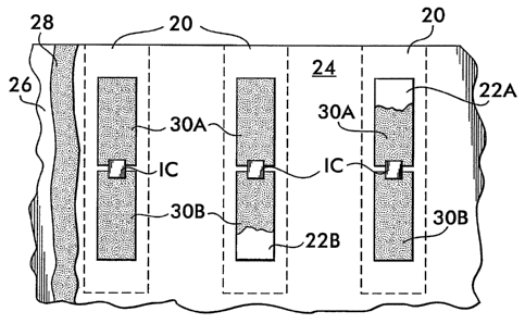
Fig. 3 is a partial top plan view of the web holding a plurality of chip
straps of the
present invention;
Fig. 4 is an enlarged side view of the web holding a plurality of chip straps
of the
present invention;
Fig. 5 shows an inverted chip strap of the present invention as it is being
applied to a
coil or antenna;
Fig. 6A depicts an exemplary HF (high frequency) security tag created using a
chip
strap in the process of the present invention;
Fig. 6B depicts an enlargement of the chip strap coupled to the coil of the HF
security tag of Fig. 6A;
Fig. 6C depicts another exemplary HF security tag created using a chip strap
and a
capacitor strap in the process of the present invention
Fig. 6D is an equivalent circuit of Figs. 6A-6C;
Fig. 7A depicts an exemplary UHF (ultra high frequency) security tag created
using a
chip strap in the process of the present invention;
Fig. 7B depicts an equivalent circuit of the present invention;
Fig. 8 provides process diagram for the tape transfer strap process of the
present
invention; and
Fig. 9 provides an exemplary label process diagram showing how the EAS or RFID
tag or inlay can then be formed into a label that is ready for use by a
customer.
DETAILED DESCRIPTION OF THE INVENTION
As mentioned earlier, the method disclosed in the present invention is
directed to the
application of capacitor straps or chip straps to an antenna or coil. Although
the maj ority of the
figures depict the attachment of chip straps to an antenna, it should be
understood that they can
4
CA 02649039 2008-10-10
WO 2007/121114 PCT/US2007/066094
just as easily depict the attachment of capacitor straps thereto. Fig. lA
depicts an exemplary
chip strap 2, Fig. 1B depicts an exemplary capacitor strap 4 and Fig. 1C
depicts an exemplary
combined chip strap and capacitor strap 6, the details of which are disclosed
in U.S. Application
Serial No. 60/730,053 and whose entire disclosure is incorporated by reference
herein. Thus, the
method is not limited to only attaching chip straps. The term "strap" as used
throughout this
Specification includes any of these flexible-type chip straps, capacitor
straps, combined chip
strap/capacitor straps.
To facilitate the quick and efficient attachment of a plurality of straps to a
plurality of
antennas or coils (the reference number 10 meaning either an antenna or a
coil) to form an EAS
or RFID security tag or inlay, the configuration of straps depicted in Figs.
lA-1C is shown in
Fig. 2 using a chip strap by way of example only. The strap of the present
invention 20
comprises an RFID integrated circuit (IC), such as those manufactured by
Philips
Semiconductor, Texas Instruments, Impinj, STMicroelectronics, etc., but could
just as easily be
a capacitor strap or combined chip strap/capacitor strap mentioned earlier. In
particular, the IC
is electrically coupled 21 (e.g., wire bonded) to respective conductive (e.g.,
aluminum) elements
22A and 22B having a thickness, by way of example only, in the range of
approximately 5 to 60
microns. These conductive elements 22A and 22B are secured (e.g., via an
adhesive 23, such as
heat seal, water base co-polymer, polyurethane, etc.) to a non-conductive
layer or substrate 24
(e.g., a polymer). A liner 26 is attached to the opposite side of the
substrate 24 using a
removable adhesive 28; this removable adhesive is low tack and similar to what
is used on
stationary notes that are sold under the mark POST-IT and examples of such
adhesives are
Rafsec RR27 removable acrylic, orFasson UR1, R10, R195, etc.). Another
adhesive 30A/30B
(e.g., a conductive adhesive, paste, tape, etc., such as anisotropic
conductive paste from Delo
Adhesives #163, National Strach, Dupont, Locktite, Acheson, etc.) is applied
to the upper
surface 32A of the conductive elements 22A and 22B.
It should be noted that another variation in the application of the adhesive
30A/30B
where the strap 20 is a chip strap, is to apply the adhesive 30A and 30B to
the corresponding
conductive elements 22A and 22B during chip strap formation, i.e., before the
IC is electrically
connected to the conductive elements 22A and 22B. With the adhesives 30A and
30B covering
the entire upper surface 32A of the conductive elements 22A/22B, when the IC
is pressed down
and electrically connected to the respective conductive elements, the
adhesives 30A and 30B are
CA 02649039 2008-10-10
WO 2007/121114 PCT/US2007/066094
compressed and forced out from under the IC and covering over the ends of the
IC, thereby
providing additional securement of the chip to the conductive elements 22A and
22B.
As will be discussed in detail later, a plurality of these straps 20 are
provided on a single
web that forms the liner 26. As shown most clearly in Figs. 3-4, each strap 20
is severed from
its neighboring strap (see cut C), with each of the straps 20 being releasably
secured to the liner
26 via the removable adhesive layer 28. To apply an individual strap 20 to an
antenna or coil,
the strap 20 is inverted as shown in Fig. 5 and the respective conductive
elements 22A and 22B
are positioned over the corresponding connecting points on the antenna or coil
(Fig. 5) so that
the adhesive 30 comes into contact with the connecting points CP1/CP2 of the
antenna or coil.
In particular, as will be discussed in detail later, in the process, each
strap 20 is indexed to be
positioned closely adjacent a corresponding antenna or coil. By way of example
only, the
connecting points CP1/CP2 of a coil provided on a coil web 40 (a portion of
which is shown in
Fig. 5) is shown in Fig. 5. The coil web 40 comprises a plurality of coils
that are also removably
secured, by a removable adhesive 42 (e.g., similar to adhesive 23 discussed
previously including
heat seal, water base copolymer, polyurethane, etc.), to a liner 44. Thus, as
will also be
discussed later, once the strap 20 is electrically connected to the coil (or
antenna), each
completed EAS (or RFID) tag or inlay can then be removed from the liner 44 and
applied to an
item using the adhesive 42. It should be understood that the web 40 can also
represent an
antenna web where instead of a plurality of coils being releasably secured
thereon, a plurality of
antennas can be provided that are releasably secured thereon.
To electrically connect the strap 20 to the coil (or antenna), heat and
pressure are then
selectively applied (using heating elements 106A and 106B) against the liner
26 at locations
aligned with the corresponding adhesives 30A and 30B. This causes the
adhesives 30A/30B to
bond the conductive elements 22A and 22B to the antenna connecting points.
This selective
application of heat simultaneously causes the removable adhesive 28 to lose
its tack, thereby
allowing the liner 26 to be removed along with the adhesive 28. Pressure and
crimping (33 and
35) at these locations forms a good electrical connection; e.g., the shards
and sharp edges of the
crimping action create a good electrical connection. The end result is a strap
20 electrically
connected to the antenna or coil. It should be understood that it is within
the broadest scope of
the present invention to include the use of chemicals to form the connection
between the strap
20 and the antenna or coil; in that situation, pressure is applied but there
is no need to crimp.
6
CA 02649039 2008-10-10
WO 2007/121114 PCT/US2007/066094
It should be further noted that the adhesives 30A/30B could initially be
placed on the
coil or antenna, rather than on the strap 20 itself.
It should be noted that the adhesive 23 (e.g., a water-based laminating
adhesive) used in
the formation of the chip strap/capacitor strap comprises a"patterned
adhesive". In accordance
with U.S. Patent No. 6,988,666 (Appalucci, et al.), entitled "Security Tag and
Process for
Making Same" and U.S. Application Serial No. 10/998,496 entitled "A Method for
Aligning
Capacitor Plates in a Security Tag and a Capacitor Formed Thereby" filed on
November 29,
2004, and all of whose entire disclosures are incorporated by reference
herein, the conductive
elements 22A/22B are formed by applying a layer of conductive material (e.g.,
aluminum) to the
non-conductive substrate 24 (e.g., a polymer) using the patterned adhesive 23
to form a
laminate. The adhesive 23 is in the form of the conductive elements 22A/22B.
Thus, when, a
cutter (in the desired shape of the conductive elements 22A/22B) is applied
against the
conductive layer, the only portion of the conductive layer that remains
adhesively secured to the
substrate 24 is the conductive elements 22A/22B; the remaining portion of the
conductive layer
can be removed and recycled. Moreover, this same process (e.g., of using a
patterned adhesive)
may be used for the formation of the coi1202 or antenna 302A/302B (see coil or
antenna web 40
in Fig. 5) to which the chip strap/capacitor strap 20 is attached.
By way of example only, Figs. 6A-6D depict an HF security tag 200 using the
process of
the present invention and Figs. 7A-7B depict a UHF security tag 300 using the
process of the
present invention. In particular, Fig. 6A illustrates a multi-turn coi1202 to
which a chip strap 20
of the present invention is secured. It should be noted that in coupling the
chip strap 20 to the
coi1202, the adhesive layer 30A/30B also acts as an insulator to prevent
shorting the conductive
members 22A/22B to any of the coil paths other than the two to which the chip
strap 20 is
electrically coupled. Fig. 6B is an enlargement of the chip strap 20 coupled
to the coi1202. Fig.
6C illustrates another HF security tag 200A using the process of the present
invention but where
a capacitor strap 20A, in addition to the chip strap 20, is also electrically
coupled to the coi1202;
by way of example only, the HF security tag 200A requires additional
capacitance (hence, the
capacitor strap 20A) in addition to the internal capacitance provided by the
IC. Fig. 6D is an
equivalent circuit of the security of Figs. 6A-6C. Fig. 7A depicts a UHF
security tag 300
whereby a chip strap 20 is coupled between the antenna elements 302A and 302B.
Fig. 7B is an
equivalent circuit of the UHF security tag 300. As mentioned previously, the
multi-turn coi1202
and the antenna elements 302A/302B may be formed using the process disclosed
in U.S. Patent
7
CA 02649039 2008-10-10
WO 2007/121114 PCT/US2007/066094
No. 6,988,666 (Appalucci, et al.), entitled "Security Tag and Process for
Making Same" and
U.S. Application Serial No. 10/998,496 entitled "A Method for Aligning
Capacitor Plates in a
Security Tag and a Capacitor Formed Thereby" filed on November 29, 2004.
Furthermore, for antennas that operate in the UHF range, a process for forming
these
types of antennas on antenna web (similar to the web 40 shown in Fig. 5) is
disclosed in co-
pending U.S. Patent Application Serial No. 11/400,893 entitled "Process for
Making UHF
Antennas for EAS and RFID Tags and Antennas Made Thereby" filed
contemporaneously
herewith and whose entire disclosure is incorporated by reference herein. This
latter process uses
a method of producing a very thin, flexible UHF antenna which involves
providing a conductor
sheet comprising a layer of electrically conductive material (e.g., aluminum)
having a top
surface and an undersurface, and wherein the conductor sheet has a thickness
in the range of
approximately 5 to 60 microns; a liner sheet (similar to liner 44 in Fig. 5)
is provided having a
top surface; disposing the conductor sheet on the liner sheet so that the
undersurface of the
conductor sheet is releasably secured to the top surface of the liner sheet by
a releasably
securable adhesive (similar to adhesive 42 of Fig. 5) substantially
coextensive with the
conductor sheet; the conductor sheet is then formed into a shape desired for
the antenna by
bringing a cutting die having the desired shape into engagement with the
conductor sheet,
whereupon the die pierces through the conductor sheet, but not through the
liner sheet, thereby
creating a die cut antenna having the desired shape secured to the liner
sheet. The waste
material is removed between adjacent antennas formed in this process (thereby
leaving a space
46, as shown in Fig. 5) and an antenna web (see web 40 in Fig. 5, as well as
reference number
104 in Fig. 8). Alternatively, where even smaller thicknesses (e.g., less than
25 microns) of the
conductor sheet of electrically conductive material are used, the conductor
sheet is first fixedly
secured to a reinforcing sheet (e.g., paper such as bond, offset, densified
kraft, or any having the
ability to support the conductor, or together form a supported composite
material and having a
thickness of approximately 50 microns as a composite, or 6 to 15 microns by
itself) and the
undersurface of that reinforcing sheet is then releasably secured to the top
surface of the liner
sheet; when the cutting die is applied, the die cuts through both the
conductor sheet and the
reinforcing sheet.
In order to create a plurality of security tags using these straps 20, Fig. 8
depicts the
process 100. In particular, a strap roll 102 and an antenna/coil roll 104
(comprising the coil or
antenna web 40) are indexed accordingly and fed between the heating elements
106 and roller
8
CA 02649039 2008-10-10
WO 2007/121114 PCT/US2007/066094
(or anvil) 108. As can be seen in Fig. 8, the antenna/coil ro11104 is oriented
so that the antennas
302 or coils 202 are facing upward and the straps 20 are facing downward
(although these
relative positions are by way of example only; the antennas could be facing
downward and the
straps could be facing upward, etc.). Depending on the security tag being
formed, the indexing
is necessary to ensure that a strap 20 is properly positioned at the coil or
antenna contact points
CP 1/CP2 when coupled thereto. In particular, the distance between adjacent
coils 202 /antenna
302 on the roll 104 is typically different than the spacing between adj acent
straps 20 on the strap
roll 102. Thus, dispensing of straps 20 from the strap ro11102 is paused as
the proper alignment
of the corresponding coil 202 or antenna 302 is made before the heating
elements 106/roller 108
are operated. Once the heating elements 106/roller 108 are activated, the
liner 26 is taken up by
a take-up reel 110. With the strap 20 properly applied to the coi1202 or
antenna elements 302,
mechanical welding (e.g., crimping) is applied at station 112, as explained
previously with
regard to Fig. 5, thereby forming a particular security tag or inlay. The term
"inlay" as used
throughout this Specification means that the completed tag (e.g., EAS or RFID
security tag) may
themselves either form a portion of a label or be coupled to a label for use
on, or otherwise
associated with, an item. The tags/inlays are gathered on a security tag or
inlay reel 114.
At this point, the tag/inlay reel 114 comprises a plurality of tags/inlays
that are exposed.
It should be understood that there are many different ways to "finish" off the
tags/inlays to form
a"label" that can be applied to an item and that it is within the broadest
scope of the invention
to include any of these. By way of example only, Fig. 9 depicts one of these
exemplary label
processes 400 in which the tag/inlays of reel 114 are made into labels. In
particular, a reel of
printable paper 116 is fed through a printing station 128 (including a roller
or anvil 130) to
provide the desired label printing onto the paper. If the paper on the reel
116 is adhesively
secured to liner 117, then the liner is removed by a take-up reel 119; if, on
the other hand, there
is no liner 117, an adhesive 121 (e.g., such as a STD acrylic, or rubber-based
hot melt adhesive)
is applied to the paper. This paper is then applied on top of the plurality of
tags/inlays from the
reel 114 at station 123 to form a label matrix 125. Next, the label matrix 125
is then sent to a
cutter 124 and roller (or anvil) 126. A take-up reel 127 removes the waste
from the label matrix
125, resulting in the label product 150, ready for application on the various
items.
Alternatively, as mentioned earlier where the coil/antenna web 40 is formed
using a
patterned adhesive, the antenna/coil web 40 requires application to a separate
liner from which
the tags/inlays can be removed. In particular, a reel 129 comprising a liner
131 has its cover
9
CA 02649039 2008-10-10
WO 2007/121114 PCT/US2007/066094
sheet 133 removed by a take-up reel 135 to expose an adhesive thereon;
alternatively, if the liner
131 has no cover sheet and adhesive, an adhesive can be applied to the liner
at station 137. In
either case, at station 139, the liner is then adhesively secured to the
bottom of the coil/antenna
web 40 from reel 114 to form a tag/inlay and liner product that is fed to the
paper application
stage 123. The process then continues as discussed previously.
It should be noted that the reel 116 is by way of example only and that the
adhesive 120
could be applied directly to the completed tags/inlays 122 and then a
printable paper 118 applied
on top of the adhesive 120.
It should be noted that where a capacitor strap and a chip strap are being
secured to a
common coil or antenna (see Fig. 6C), the process shown in Fig. 8 is
supplemented with a third
web (not shown) which is then indexed also with the antenna web 104. It should
be understood
that either type of strap (chip strap or capacitor strap) could be applied
before the other in the
process. In addition a second take up reel (not shown) would also be present
to take up the
released liner from the web of capacitor straps.
While the invention has been described in detail and with reference to
specific examples
thereof, it will be apparent to one skilled in the art that various changes
and modifications can be
made therein without departing from the spirit and scope thereof.