Note: Descriptions are shown in the official language in which they were submitted.
CA 02649472 2008-10-16
WO 2007/130771
PCT/US2007/066021
MULTIPOINT TOUCH SURFACE CONTROLLER
Background
[0001] There exist today many styles of input devices for
performing operations in a computer system. The operations generally
correspond to moving a cursor and/or making selections on a display
screen. By way of example, the input devices may include buttons or keys,
mice, trackballs, touch pads, joy sticks, touch screens and the like. Touch
pads and touch screens (collectively "touch surfaces") are becoming
increasingly popular because of their ease and versatility of operation as
well as to their declining price. Touch surfaces allow a user to make
selections and move a cursor by simply touching the surface, which may
be a pad or the display screen, with a finger, stylus, or the like. In
general, the touch surface recognizes the touch and position of the touch
and the computer system interprets the touch and thereafter performs an
action based on the touch.
[0002] Of particular interest are touch screens. Various types of
touch screens are described in applicant's co-pending patent application
serial no. 10/840,862, entitled "Multipoint Touchscreen," filed May 6,
2004, which is hereby incorporated by reference in its entirety. As noted
therein, touch screens typically include a touch panel, a controller and a
software driver. The touch panel is generally a clear panel with a touch
sensitive surface. The touch panel is positioned in front of a display
screen so that the touch sensitive surface covers the viewable area of the
display screen. The touch panel registers touch events and sends these
signals to the controller. The controller processes these signals and sends
the data to the computer system. The software driver translates the touch
events into computer events.
CA 02649472 2008-10-16
WO 2007/130771
PCT/US2007/066021
[0003] There
are several types of touch screen technologies
including resistive, capacitive, infrared, surface acoustic wave,
electromagnetic, near field imaging, etc. Each of
these devices has
advantages and disadvantages that are taken into account when designing
or configuring a touch screen. One problem found in these prior art
technologies is that they are only capable of reporting a single point even
when multiple objects are placed on the sensing surface. That is, they
lack the ability to track multiple points of contact simultaneously. In
resistive and traditional capacitive technologies, an average of all
simultaneously occurring touch points are determined and a single point
which falls somewhere between the touch points is reported. In surface
wave and infrared technologies, it is impossible to discern the exact
position of multiple touch points that fall on the same horizontal or vertical
lines due to masking. In either case, faulty results are generated.
[0004] These
problems are particularly problematic in handheld
devices, such as tablet PCs, where one hand is used to hold the tablet and
the other is used to generate touch events. For example, as shown in
Figs. 1A and 1B, holding a tablet 2 causes the thumb 3 to overlap the
edge of the touch sensitive surface 4 of the touch screen 5. As shown in
Fig. 1A, if the touch technology uses averaging, the technique used by
resistive and capacitive panels, then a single point that falls somewhere
between the thumb 3 of the left hand and the index finger 6 of the right
hand would be reported. As shown in Fig. 1B, if the technology uses
projection scanning, the technique used by infrared and surface acoustic
wave panels, it is hard to discern the exact vertical position of the index
finger 6 due to the large vertical component of the thumb 3. The tablet 2
can only resolve the patches shown in gray. In essence, the thumb 3
masks out the vertical position of the index finger 6.
[0005] While
virtually all commercially available touch screen based
systems available today provide single point detection only and have
- 2 -
CA 02649472 2008-10-16
WO 2007/130771
PCT/US2007/066021
limited resolution and speed, other products available today are able to
detect multiple touch points. Unfortunately, these products only work on
opaque surfaces because of the circuitry that must be placed behind the
electrode structure. Examples of such products include the Fingerworks
series of touch pad products. Historically, the number of points detectable
with such technology has been limited by the size of the detection
circuitry.
[0006] Therefore, what is needed in the art is a multi-touch capable
touch screen controller that facilitates the use of transparent touch
sensors and provides for a conveniently integrated package.
Summary
[0007] A controller for multi-touch touch surfaces is disclosed
herein. One aspect of the multi-touch touch surface controller relates to
the integration of drive electronics for stimulating the multi-touch sensor
and sensing circuits for reading the multi-touch sensor into a single
integrated package.
[0008] Another aspect of the controller relates to a technique for
suppressing noise in the sensor by providing a plurality of stimulus
waveforms to the sensor wherein the waveforms have different
frequencies. This permits at least one noise-free detection cycle in cases
where noise appears at a particular frequency.
[0009] Another aspect of the controller relates to a charge amplifier
that includes programmable components, namely, programmable resistors
and capacitors to allow the circuit to be easily reconfigured to provide
optimum sensing configurations for a variety of sensor conditions.
[0010] Another aspect of the controller relates to an offset
compensation circuit that expands the dynamic range of the controller by
eliminating a static portion of the multi-touch surface sensor output
- 3 -
CA 02649472 2012-04-12
allowing the full dynamic range of the sensing circuitry to be allocated to
the
changing portions of the output signal.
[0011] Another aspect of the controller relates to a demodulation circuit
that
enhances the noise immunity of the sensor arrangement by application of
particular demodulation waveforms known to have particular frequency
characteristics.
[0012] Another aspect of the controller relates to the application of
various
algorithms to the sensor outputs obtained from the multiple stimulus
frequencies
described above to further increase noise immunity of the system.
[0012a] In a further aspect, the present invention provides a controller
for
touch surface, the touch surface having a plurality of drive electrodes and at
least
one sense electrode, a plurality of nodes formed at intersections of the
plurality of
drive electrodes and the at least one sense electrode, the controller
comprising:
output circuitry operatively connected to the plurality of drive electrodes,
the output
circuitry being configured to generate timing signals used to generate drive
waveforms for the touch surface, each drive waveform including a plurality of
bursts in a single stimulation sequence for stimulating the drive electrodes
in a
single scan of the nodes in the touch surface, the plurality of bursts
including a first
periodic waveform having a first predetermined frequency, and at least one
additional periodic waveform having at least one additional predetermined
frequency different from the first predetermined frequency; and input
circuitry
operatively connected to the at least one sense electrode, the input circuitry
being
configured to determine proximity of an object at each node by measuring
capacitive coupling of the drive waveforms from the drive electrode to the
sense
electrode of the node; wherein at least one of the drive electrodes is
stimulated
consecutively with the plurality of bursts including periodic waveforms having
different predetermined frequencies before one of the other drive electrodes
is
stimulated.
- 4 -
CA 02649472 2012-04-12
[001213] In a still further aspect, the present invention provides a method
of
operating a touch surface, the touch surface comprising a plurality of drive
electrodes and at least one sense electrode, a plurality of nodes formed at
intersections of the plurality of drive electrodes and the at least one sense
electrode, the method comprising: stimulating the drive electrodes with a
plurality
of bursts in a single stimulation sequence in a single scan of the nodes in
the touch
surface, the plurality of bursts including first periodic waveform having a
first
predetermined frequency and at least one additional periodic waveform having
an
additional predetermined frequency different from the first predetermined
frequency; reading the at least one sense electrode after the drive electrodes
have
been stimulated with the first periodic waveform during the single scan to
determine a first capacitance of the nodes formed at the intersection of the
drive
electrodes and the at least one sense electrode; reading the at least one
sense
electrode after the drive electrodes have been stimulated with an additional
periodic waveform during the single scan to determine at least one additional
capacitance of the node formed at the intersection of the drive electrode and
the at
least one sense electrode; and combining the first capacitance with the at
least
one additional capacitance to determine a true capacitance of the node,
wherein at
least one of the drive electrodes is stimulated consecutively with the
plurality of
bursts including periodic waveforms having different predetermined frequencies
before one of the other drive electrodes is stimulated.
[0012c1 In a still further aspect, the present invention provides a method
of
operating a touch surface, the touch surface comprising a plurality of drive
electrodes and at least one sense electrode, a plurality of nodes formed at
intersections of the plurality of drive electrodes and the at least one sense
electrode, the method comprising: stimulating the drive electrodes with a
plurality
of bursts in a single stimulation sequence in a single scan of the nodes in
the touch
surface, the plurality of bursts including a first drive waveform having a
first
- 4a -
CA 02649472 2012-04-12
predetermined frequency and at least one additional drive waveform having at
least one additional predetermined frequency different from the first
predetermined
frequency; detecting a first waveform on the at least one sense electrode
caused
by capacitive coupling of a drive waveform at the nodes; detecting at least
one
additional waveform on the at least one sense electrode caused by capacitive
coupling of the at least one additional drive waveform at the nodes;
amplifying the
detected waveforms; and demodulating each of the first waveform and the at
least
one additional waveform; determining a capacitance at the nodes to detect an
object located proximate the node, wherein at least one of the drive
electrodes is
stimulated consecutively by the plurality of bursts including periodic
waveforms
having different predetermined frequencies before one of the other drive
electrodes
is stimulated.
[0013] These and other aspects will be more readily understood by
reference to the following detailed description and figures.
Brief Description of the Drawings
[0014[ Figures I A and I B illustrates certain problems with prior art
touch
screen technologies.
[0015] Figure 2 illustrates a perspective view of a computing device
incorporating a multi-touch touch screen and multi-touch touch screen
controller
according to certain teachings of the present disclosure.
[0016] Figure 3 is a block diagram of a computing device incorporating a
multi-touch touch screen and multi-touch touch screen controller according to
certain teachings of the present disclosure.
[0017] Figures 4A and 4B illustrate two possible arrangement of drive and
sense electrodes in a multi-touch touch surface.
- 4b -
CA 02649472 2012-04-12
[0018] Figure
5 is a layer diagram illustrating communication between the
multi-touch surface and the host computer device by way of a multi-touch
controller incorporating various teachings of the present disclosure.
- 4c -
CA 02649472 2008-10-16
WO 2007/130771
PCT/US2007/066021
[0019] Figure 6 is an equivalent circuit showing the output circuitry
of the controller, a cell of the multi-touch sensor, and the input circuitry
of
a multi-touch controller incorporating various teachings of the present
disclosure.
[0020] Figure 7 is a circuit schematic of a charge amplifier
incorporated in certain embodiments of a multi-touch controller
incorporating various teachings of the present disclosure.
[0021] Figure 8 is a block diagram of the multi-touch surface and
multi-touch controller system in accordance with various teachings of the
present disclosure.
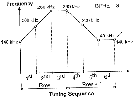
[0022] Figure 9 illustrates the sequence in which drive waveforms of
varying frequencies are applied to the multi-touch sensor in accordance
with certain teachings of the present disclosure.
[0023] Figure 10 is a block diagram illustrating the input circuitry
of
a multi-touch controller incorporating certain teachings of the present
disclosure.
[0024] Figures 11A and 11B illustrate various demodulation
waveforms together with frequency spectra of their passbands.
[0025] Figure 12 illustrates a sequence of stimulus waveforms,
together with a particular demodulation waveform, and the resulting
output.
[0026] Figure 13 illustrates the noise rejection technique employed
by the majority rules algorithm.
Detailed Description
[0027] A
multipoint touch screen controller (MTC) is described
herein. The following embodiments of the invention, described in terms of
devices and applications compatible with computer systems manufactured
- 5 -
CA 02649472 2008-10-16
WO 2007/130771
PCT/US2007/066021
by Apple Computer, Inc. of Cupertino, California, are illustrative only and
should not be considered limiting in any respect.
[0028] Fig. 2
is a perspective view of a touch screen display
arrangement 30. Display arrangement 30 includes a display 34 and a
transparent touch screen 36 positioned in front of display 34. Display 34
may be configured to display a graphical user interface (GUI) including
perhaps a pointer or cursor as well as other information to the user.
Transparent touch screen 36 is an input device that is sensitive to a user's
touch, allowing a user to interact with the graphical user interface on
display 34. In general, touch screen 36 recognizes touch events on
surface 38 of touch screen 36 and thereafter outputs this information to a
host device. The host device may, for example, correspond to a computer
such as a desktop, laptop, handheld or tablet computer. The host device
interprets the touch event and thereafter performs an action based on the
touch event.
[0029] In
contrast to prior art touch screens, touch screen 36 shown
herein is configured to recognize multiple touch events that occur
simultaneously at different locations on touch sensitive surface 38. That
is, touch screen 36 allows for multiple contact points T1¨T4 to be tracked
simultaneously. Touch screen 36 generates separate tracking signals S1¨
S4 for each touch point T1¨T4 that occurs on the surface of touch screen
36 at the same time. In one embodiment, the number of recognizable
touches may be about 15 which allows for a user's 10 fingers and two
palms to be tracked along with 3 other contacts. The multiple touch
events can be used separately or together to perform singular or multiple
actions in the host device. Numerous examples of multiple touch events
used to control a host device are disclosed in U.S. Patents 6,323,846;
6,888,536; 6,677,932; 6,570,557, and co-pending U.S. patent applications
11/015,434; 10/903,964; 11/048,264; 11/038,590; 11/228,758;
- 6 -
CA 02649472 2008-10-16
WO 2007/130771
PCT/US2007/066021
11/228,700; 11/228,737; 11/367,749, each of which is hereby
incorporated by reference in its entirely.
[0030] Fig. 3
is a block diagram of a computer system 50,
employing a multi-touch touch screen. Computer system 50 may be, for
example, a personal computer system such as a desktop, laptop, tablet, or
handheld computer. The computer system could also be a public
computer system such as an information kiosk, automated teller machine
(ATM), point of sale machine (POS), industrial machine, gaming machine,
arcade machine, vending machine, airline e-ticket terminal, restaurant
reservation terminal, customer service station, library terminal, learning
device, etc.
[0031] Computer
system 50 includes a processor 56 configured to
execute instructions and to carry out operations associated with the
computer system 50. Computer code and data required by processor 56
are generally stored in storage block 58, which is operatively coupled to
processor 56. Storage block 58 may include read-only memory (ROM) 60,
random access memory (RAM) 62, hard disk drive 64, and/or removable
storage media such as CD-ROM, PC-card, floppy disks, and magnetic
tapes. Any of these storage devices may also be accessed over a network.
Computer system 50 also includes a display device 68 that is operatively
coupled to the processor 56. Display device 68 may be any of a variety of
display types including liquid crystal displays (e.g., active matrix, passive
matrix, etc.), cathode ray tubes (CRT), plasma displays, etc.
[0032] Computer
system 50 also includes touch screen 70, which is
operatively coupled to the processor 56 by I/O controller 66 and touch
screen controller 76. (The I/O controller 66 may be integrated with the
processor 56, or it may be a separate component.) In any case, touch
screen 70 is a transparent panel that is positioned in front of the display
device 68, and may be integrated with the display device 68 or it may be a
separate component. Touch screen 70 is configured to receive input from
- 7 -
CA 02649472 2008-10-16
WO 2007/130771
PCT/US2007/066021
a user's touch and to send this information to the processor 56. In most
cases, touch screen 70 recognizes touches and the position and
magnitude of touches on its surface.
[0033] Better understanding of the interface between the touch
sensor and the host computer system may be had with reference to Fig. 5,
which is a layer diagram of the system illustrated in Fig. 3. The touch
sensor 301 resides at the lowermost layer. In a preferred embodiment,
the sensor interfaces with an ASIC (application specific integrated circuit)
305 that stimulates the sensor and reads the raw sensor output as
described in more detail below. ASIC 305 interfaces via signaling 306 with
a DSP (digital signal processor) and/or microcontroller 307, which
generates the capacitance images. Together ASIC 305 and
DSP/microcontroller 307 form the multipoint touch screen controller.
[0034] DSP/Microcontroller 307 includes an interface 308 for
accepting the signaling 306 from ASIC 305, and these signals are then
passed to a data capture and error rejection layer 309. Data from this
layer may be accessed both for calibration, baseline and standby
processing by module 310, as well as feature (Le., touch point) extraction
and compression module 311. Once the features are extracted they are
passed as high-level information to the host computer 302 via interface
303. Interface 303 may be, for example, a USB (universal serial bus)
interface. Alternatively, other forms of interface, such as IEEE 1394
("Firewire"), RS-232 serial interface, SCSI (small computer systems
interface), etc. could be used.
[0035] The exact physical construction of the sensing device is not
necessary for a complete understanding touch screen controller disclosed
herein. Nonetheless, details of the construction may be understood by
reference to the patents and patent applications incorporated by reference
above. For purposes of the present description, the sensor may be
- 8 -
CA 02649472 2008-10-16
WO 2007/130771
PCT/US2007/066021
assumed to be a mutual capacitance device constructed as described
below with reference to Figs. 4A and 4B.
[0036] The
sensor panel is comprised of a two-layered electrode
structure, with driving lines on one layer and sensing lines on the other.
In either case, the layers are separated by a dielectric material. In the
Cartesian arrangement of Fig. 4A, one layer is comprised of N horizontal,
preferably equally spaced row electrodes 81, while the other layer is
comprised of M vertical, preferably equally spaced column electrodes 82.
In a polar arrangement, illustrated in Fig. 4B, the sensing lines may be
concentric circles and the driving lines may be radially extending lines (or
vice versa). As will be appreciated by those skilled in the art, other
configurations based on an infinite variety of coordinate systems are also
possible.
[0037] Each
intersection 83 represents a pixel and has a
characteristic mutual capacitance, CSIG. A grounded object (such as a
finger) that approaches a pixel 83 from a finite distance shunts the electric
field between the row and column intersection, causing a decrease in the
mutual capacitance CSIG at that location. In the case of a typical sensor
panel, the typical signal capacitance CSIG is about 0.75pF and the change
induced by a finger touching a pixel, is about 0.25pF.
[0038] The
electrode material may vary depending on the
application. In touch screen applications, the electrode material may be
ITO (Indium Tin Oxide) on a glass substrate. In a touch tablet, which
need not be transparent, copper on an FR4 substrate may be used. The
number of sensing points 83 may also be widely varied. In touch screen
applications, the number of sensing points 83 generally depends on the
desired sensitivity as well as the desired transparency of the touch screen
70. More nodes or sensing points generally increases sensitivity, but
reduces transparency (and vice versa).
- 9 -
CA 02649472 2008-10-16
WO 2007/130771
PCT/US2007/066021
[0039] During
operation, each row (or column) is sequentially
charged by driving it with a predetermined voltage waveform 85
(discussed in greater detail below). The charge capacitively couples to the
columns (or rows) at the intersection. The
capacitance of each
intersection 83 is measured to determine the positions of multiple objects
when they touch the touch surface. Sensing circuitry monitors the charge
transferred and time required to detect changes in capacitance that occur
at each node. The positions where changes occur and the magnitude of
those changes are used to identify and quantify the multiple touch events.
Driving each row and column and sensing the charge transfer is the
function of a multipoint touch screen controller.
[0040] Fig. 6
is a simplified diagram of the equivalent mutual
capacitance circuit 220 for each coupling node. Mutual capacitance circuit
220 includes a driving line 222 and a sensing line 224 that are spatially
separated thereby forming a capacitive coupling node 226. When no
object is present, the capacitive coupling at node 226 stays fairly constant.
When an object, such as a finger, is placed proximate the node 226, the
capacitive coupling through node 226 changes. The object effectively
shunts the electric field so that the charge transferred across node 226 is
less.
[0041] With
reference to Figs. 5 and 8, ASIC 305 generates all the
drive waveforms necessary to scan the sensor panel. Specifically, the
microprocessor sends a clock signal 321 to set the timing of the ASIC,
which in turn generates the appropriate timing waveforms 322 to create
the row stimuli to the sensor 301. Decoder 311 decodes the timing
signals to drive each row of sensor 301 in sequence. Level shifter 310
converts timing signals 322 from the signaling level (e.g., 3.3V) to the
level used to drive the sensor (e.g., 18V).
[0042] Each row of the sensor panel is driven determined by
microprocessor 307. For noise rejection purposes it is desirable to drive
- 10 -
CA 02649472 2008-10-16
WO 2007/130771
PCT/US2007/066021
the panel at multiple different frequencies for noise rejection purposes.
Noise that exists at a particular drive frequency may not, and likely will not
exist at the other frequencies. In a preferred embodiment, each sensor
panel row is stimulated with three bursts of twelve square wave cycles
(50% duty-cycle, 18V amplitude), while the remaining rows are kept at
ground. For better noise rejection, described in greater detail below the
frequency of each burst is different, exemplary burst frequencies are
140kHz, 200kHz, and 260Khz.
[0043] During each burst of pulses ASIC 305 takes a measurement
of the column electrodes. This process is repeated for all remaining rows
in the sensor panel. The results are three images, each image taken at a
different stimulus frequency.
[0044] Additionally, it is preferable to minimize the amount of
stimulus frequency change required for each subsequent burst. Therefore
a frequency hopping pattern that minimizes the changes is desirable.
Figure 29 shows one possible frequency hopping pattern. In this
arrangement, a first row is driven with a 140 kHz burst, then a 200 kHz,
and finally a 260 kHz burst. Then a next row is driven with three bursts at
260 kHz, 200 kHz, and 140 kHz, respectively. This particular frequency
pattern was chosen to keep changes between frequencies small and allow
the frequency transitions have to be smooth and glitch free. However,
other frequency hopping arrangements are also possible, including
scanning more than three frequencies, scanning the frequencies in a
quasi-random sequence rather than the ordered pattern described, and
adaptive frequency hopping, in which the scan frequencies are selected
based on the noise environment.
[0045] Turning back to Fig. 6, sensing line 224 is electrically
coupled
to a capacitive sensing circuit 230. Capacitive sensing circuit 230 detects
and quantifies the current change and the position of the node 226 where
the current change occurred and reports this information to a host
- 11 -
CA 02649472 2008-10-16
WO 2007/130771
PCT/US2007/066021
computer. The signal of interest is the capacitance CSIG, which couples
charge from RC network A to RC network B. The output from RC network
B connects directly to the analog input terminals of ASIC 305. ASIC 305
also uses the clock signal 321 (Fig. 8) from microprocessor 307 (Fig. 8) to
time the detection and quantification of the capacitance signals.
[0046] Figure
10 is a block diagram illustrating the input stage of
ASIC 305. The input signal is first received by a charge amplifier 401.
The charge amplifier performs the following tasks: (1) charge to voltage
conversion, (2) charge amplification, (3) rejection or stray capacitance
present at the column electrode, and (4) anti aliasing, and (5) gain
equalization at different frequencies. Figure 7 is a diagram of one possible
charge amplifier 401.
[0047] Charge
to voltage conversion is performed by a capacitor CFB
in the feedback path of an operational amplifier 450. In one embodiment,
the feedback capacitor can be programmed with values ranging from 2 to
32 pF, which allows the output voltage level to be adjusted to obtain the
best dynamic range for a range of CsiG values. The feedback resistor RFB
is also preferably programmable to control the amplifier gain.
[0048] Because
CsIG will vary across a touch surface because of a
variety of manufacturing tolerance related factors, it is useful to adjust the
charge amplifier feedback capacitance CFB on a per-pixel basis. This
allows gain compensation to be performed to optimize the performance of
each pixel. In one embodiment, quasi-per pixel adjustment is performed
as follows: The feedback capacitor CFB has its value set by a register
known as CFB_REG. The value of CFB_REG is set according to the
following equation:
CFB_REG[Y] =CFB_UNIV+CFB[Y]
where Y is an individual pixel within a row, CFB_UNIV is adjusted on a row
by row basis, and CFB[Y] is a lookup table loaded at system startup. In
alternative arrangements, CFB_UNIV may be constant for all rows, or the
- 12 -
CA 02649472 2012-04-12
CFB[Y] lookup table may be switched out on a row by row basis. Also, although
discussed in terms of rows and columns, the adjustment arrangement is equally
applicable to non-Cartesian coordinate systems.
[0049] Obviously it is desirable to measure Cs1G while rejecting as much
as
possible the effects of any parasitic resistance and capacitance in the
physical
sensor. Rejection of parasitic resistance and capacitance in the sensor may be
accomplished by holding the non-inverting input 451 of amplifier 450 at a
constant
value, e.g., ground. The inverting input 452 is coupled to the node being
measured. As will be appreciated by those skilled in the art, inverting input
452
(connected to the column electrode being measured) is thus held at virtual
ground.
Therefore any parasitic capacitance present at the column electrode, e.g., PCB
stray capacitance or dynamic stray capacitance caused by the user touching the
column electrode, is rejected because the net charge of the stray capacitor
does
not change (i.e., the voltage across the stray capacitance is held at virtual
ground).
Therefore the charge amplifier output voltage 453 is only a function of the
stimulus
voltage, CSIG, and CFB. Because the stimulus voltage and CFB are determined by
the controller, CsiG may be readily inferred.
[0050] A series resistor 454 between the ASIC input pin 455 and the
inverting input 452 of the charge amplifier forms an anti-aliasing filter in
combination with the feedback network of RFB and CFB.
[0051] The high pass roll off of the charge amplifier is set by the
parallel
combination of the feedback resistor RFB and the feedback capacitor CF12.=
[0052] Again with reference to Fig. 10, the output of charge amplifier
401
passes to demodulator 403. Demodulator 403 is a 5-bit quantized continuous
time
analog (four-quadrant) multiplier. The purpose of demodulator 403
is to reject out of band noise sources (from cell phones,
microwave ovens, etc.) that are present on the signal entering
-13-
CA 02649472 2008-10-16
WO 2007/130771
PCT/US2007/066021
ASIC 305. The output 402 of the charge amplifier (VsiG) is mixed with a 5-
bit quantized waveform that is stored in a lookup table 404. The shape,
amplitude, and frequency of the demodulation waveform is determined by
programming suitable coefficients into lookup table 404. The
demodulation waveform determines pass band, stop band, stop band
ripple and other characteristics of the mixer. In a preferred embodiment,
Gaussian shaped sine wave is used as the demodulation waveform. A
Gaussian sine wave provides a sharp pass band with reduced stop band
ripple.
[0053] Another aspect of demodulator 403 relates to demodulator
phase delay adjustment. As can be seen with reference to Fig. 10, the
touch surface electrodes can be represented by a RC networks (RC
Network A and RC Network B) that have a mutual capacitance (CsiG) at
the point they intersect. Each RC network constitutes a low pass filter,
while CSIG introduces a high pass filter response. Therefore the touch
panel looks like a bandpass filter, only allowing signals with a certain
frequency ranges to pass the panel. This frequency range, i.e., those
frequencies that are below the cutoff of CMG but above the cutoff of RC
Networks A and B, determines the stimulus frequencies that may be used
to drive the touch panel.
[0054] The panel will therefore impose a phase delay on the
stimulus waveform passing through it. This phase delay is negligible for
traditional opaque touch panels, wherein the electrode structure is
typically formed by PCB traces, which have negligible resistance to their
characteristic impedance. However, for transparent panels, typically
constructed using Indium Tin Oxide (ITO) conductive traces, the resistive
component may be quite large. This introduces a significant time (phase)
delay in the propagation of the stimulus voltage through the panel. This
phase delay causes the demodulation waveform to be delayed with
- 14 -
CA 02649472 2008-10-16
WO 2007/130771
PCT/US2007/066021
respect to the signal entering the pre-amplifier, thereby reducing the
dynamic range of the signal coming out of the ADC.
[0055] To compensate for this phase delay, a delay clock register
("DCL", not shown) may be provided, which can be used to delay the
demodulation waveform relative to the signal entering the preamplifier
therefore compensating for the external panel delay and maximizing the
dynamic range. This register is input into the demodulator 403 and simply
delays the demodulation waveform by a predetermined amount. The
amount may be determined either on startup of the panel by
measurement, or may be estimated for the panel as a whole based on
known manufacturing characteristics. Each pixel of the touch surface may
have its own uniquely determined delay parameter to fully optimize the
reading circuitry, or the delay parameter may be determined on a row by
row basis. Adjustment would be generally similar to the techniques
discussed above for adjustment of the charge amplifier feedback capacitor
and the offset compensation voltage.
[0056] The demodulated signal is then passed to offset
compensation circuitry. The offset compensation circuitry comprises mixer
402 and programmable offset DAC 405. Mixer 402 takes the output
voltage 453 of the demodulator and subtracts an offset voltage (discussed
below) to increase the dynamic range of the system.
[0057] Offset compensation is necessary because the pixel
capacitance CSIG is comprised of a static part and a dynamic part. The
static part is a function of sensor construction. The dynamic part is a
function of the change of CSIG when the finger approaches the pixel, and is
thus the signal of interest. The purpose of the offset compensator is to
eliminate or minimize the static component thereby extending the dynamic
range of the system.
[0058] As noted above, the offset compensation circuitry is
comprised of two parts, a programmable offset DAC 405 and a mixer 402.
- 15 -
CA 02649472 2008-10-16
WO 2007/130771
PCT/US2007/066021
Offset DAC 405 generates a programmable offset voltage from the digital
static offset value VOFF_REG. This digital value is converted into a static
analog voltage (or current, if operating in the current domain) by the DAC
and then mixed (by mixer 403b) with a voltage (or current) set by the
absolute value (determined by block 404b) of the demodulation waveform.
The result is a rectified version of the demodulation waveform, the
amplitude of which is set by the static value of VOFF_REG and the
absolute portion of the demodulation waveform currently retrieved from
the DMOD lookup table 404. This allows for the right amount of offset
compensation for a given portion of the demodulation waveform.
Therefore the offset compensation waveform effectively tracks the
demodulation waveform.
[0059] As with
the charge amplifier feedback capacitor, it is useful
to adjust the offset compensation circuitry to account for variations in the
individual pixel capacitance due to manufacturing tolerances, etc. The
adjustment may be substantially similar to that discussed above with
respect to the charge amplifier feedback capacitor. Specifically, the offset
voltage value stored in VOFF_REG may be calculated as follows:
VOFF_REG [Y] = VOFF_U N IV+ VOFF[Y]
where Y is the individual column within a row, VOFF_UNIV is an offset
voltage set on a row by row basis, and VOFF[Y] is a lookup table. Again,
the adjustment could be performed on a true pixel by pixel basis or
VOFF_UNIV could be a single constant value, depending on a particular
implementation. Also, although discussed in terms of rows and columns,
the adjustment arrangement is equally applicable to non-Cartesian
coordinate systems.
[0060] As an
alternative to the arrangement described above with
respect to Fig. 10, the offset compensation could take place prior to
demodulation. In this
case, the shape of the offset compensation
waveform has to match the waveform coming out of the preamplifier
- 16 -
CA 02649472 2008-10-16
WO 2007/130771
PCT/US2007/066021
rather than the waveform coming out of the demodulator, Le., it has to be
a square wave, assuming negligible attenuation in the panel, such that the
shape of the drive waveform is preserved. Also, if offset compensation is
performed first, the offset waveform is an AC waveform with respect to
the reference voltage, Le., the maxima are positive in respect to VREF and
the minima are negative in respect to VREF. The amplitude of the offset
waveform is equivalent to the amount of offset compensation.
Conversely, if demodulation is performed first, the offset waveform is a DC
waveform, i.e. it is either positive in respect to Vref or negative (since the
demodulated waveform is also DC in respect to Vref). Again, the amplitude
in this case is equivalent to the amount of offset compensation for every
part of the demodulated waveform. In essence, the offset compensation
circuit needs to correlate the amount of offset compensation needed
dependent on the shape of the waveform.
[0061] The demodulated, offset compensated signal is then
processed by programmable gain ADC 406. In one embodiment, ADC 406
may be a sigma-delta, although similar type ADCs (such as a voltage to
frequency converter with a subsequent counter stage) could be used. The
ADC performs two functions: (1) it converts the offset compensated
waveform out of the mixer arrangement (offset and signal mixer) to a
digital value; and (2) it performs low pass filtering functions, i.e., it
averages the rectified signal coming out of the mixer arrangement. The
offset compensated, demodulated signal looks like a rectified Gaussian
shaped sine wave, whose amplitude is a function of CFB and CsIG. The ADC
result returned to the host computer is actually the average of that signal.
[0062] One advantage of using a sigma delta ADC is that such ADCs
are much more efficient for performing averaging in the digital domain.
Additionally, digital gates are a lot smaller than analog low pass filters and
sample and hold elements, thus reducing the size of the total ASIC. One
- 17 -
CA 02649472 2008-10-16
WO 2007/130771
PCT/US2007/066021
skilled in the art will further appreciated other advantages, particularly
with regard to power consumption and clock speed.
[0063]
Alternatively, one could use an ADC separate from the
controller ASIC. This would require a multiplexor to share the ADC
between multiple channels and a sample and hold circuit for each channel
to average and hold the average of the demodulation waveform. This
would likely consume so much die area as to be impractical for controllers
intended for use with touch surfaces having a large number of pixels.
Additionally, to achieve acceptable operation, the external ADC would
need to operate very fast, as a large number of pixels must be processed
very quickly to provide timely and smooth results in response to a user's
input.
[0064] As noted
above, the sensor is driven at three different
frequencies, resulting in three capacitance images, which are used for
noise rejection as described below. The three frequencies are chosen
such that the pass band at one particular frequency does not overlap with
the pass bands at the other frequencies. As noted above, a preferred
embodiment uses frequencies of 140 kHz, 200 kHz, and 240 kHz. The
demodulation waveform is chosen such that the side bands are
suppressed.
[0065] As noted
above, a Gaussian enveloped sine wave, illustrated
in Fig. 11A together with its passband frequency spectrum, is one
preferred demodulation waveform. The Gaussian shaped sine wave
provides a well-defined pass band with minimum stop band ripple.
Alternatively, other waveforms having well defined pass bands with
minimum stop band ripple could also be used. For example, a ramp-
enveloped sine wave, illustrated in Fig. 11B together with its passband
frequency spectrum, also has a well defined pass band, although the stop
band ripple is slightly greater than that for a Gaussian enveloped sine
- 18 -
CA 02649472 2008-10-16
WO 2007/130771
PCT/US2007/066021
wave. As will be appreciated by those skilled in the art, other waveforms
could also be used.
[0066] Turning now to Fig. 12, nine waveforms are illustrated that
explain the noise suppression features of the system. Voltage waveform
501 is a square wave demonstrating the stimulus waveform applied to the
sensor. Waveform 504 is the Gaussian enveloped sine wave signal used
as a demodulation waveform. Waveform 507 is the output of the
demodulator, i.e., the product of the waveforms 501 and 504. Note that it
provides a well defined pulse at the fundamental frequency of the applied
square wave voltage.
[0067] The center column illustrates an exemplary noise waveform
502. Demodulation waveform 505 is the same as demodulation waveform
504. Note that the demodulated noise signal 508 does not produce a
significant spike, because the fundamental frequency of the noise signal is
outside the passband of the demodulation signal.
[0068] The composite of the excitation waveform and noise signal is
illustrated in 503. Again, demodulation waveform 506 is the same as
demodulation waveforms 505 and 504. The demodulated composite does
still show the noise waveform, although various signal processing
algorithms may be applied to extract this relatively isolated spike.
[0069] Additionally, noise rejection may accomplished by providing
multiple stimulus voltage at different frequencies and applying a majority
rules algorithm to the result. In a majority rules algorithm, for each
capacitance node, the two frequency channels that provide the best
amplitude match are averaged and the remaining channel is disposed of.
For example, in Fig. 13 vertical line 600 represents the measured
capacitance, with the markings 601, 602, and 603 representing the three
values measured at three stimulus frequencies. Values 602 and 603
provide the best match, possibly suggesting that value 601 is corrupted.
- 19 -
CA 02649472 2008-10-16
WO 2007/130771
PCT/US2007/066021
Thus value 601 is discarded and values 602 and 603 are averaged to form
the output.
[0070]
Alternatively, a median filter could be applied, in which case
value 602, Le., the median value would be selected as an output. As yet
another alternative, the three results could simply be averaged, in which
case a value somewhere between value 601 and 602 would result. A
variety of other noise rejection techniques for multiple sample values will
be obvious to those skilled in the art, any of which may suitably be used
with the controller described herein.
[0071]
Operation of the circuit may be further understood with
respect to Fig. 14, which is a flowchart depicting operation of the
controller. One skilled in the art will appreciate that various timing and
memory storage issues are omitted from this flowchart for the sake of
clarity.
[0072] Image
acquisition begins at block 701. The system then sets
the clock so as to acquire samples at the middle clock frequency (e.g.,
200kHz) as discussed above with respect to Fig. 9 (block 702). The
various programmable registers, which control such parameters as voltage
offset, amplifier gain, delay clocks, etc., are then updated (block 703). All
columns are read, with the result stored as a Mid Vector (block 704) The
high clock frequency is then set (block 705), and the steps of updating
registers (block 706) and reading all columns and storing the result (step
707) are repeated for the high sample frequency. The clock is then set to
the low frequency (step 708) and the register update (block 709) and
column reading (block 710) are repeated for the low sample frequency.
[0073] The
three vectors are then offset compensated, according to
the algorithm described above (block 711). The offset compensated
vectors are then subjected to a median filter as described above.
Alternatively, the offset compensated vectors could be filtered by the
majority rules algorithm described with respect to Fig. 13 or any other
- 20 -
CA 02649472 2012-04-12
suitable filtering technique. In any case, the result is stored. If more rows
remain,
the process returns to the mid frequency sampling at block 702). If all rows
are
completed (block 713), the entire image is output to the host device (block
714),
and a subsequent new image is acquired (block 701).
[0074] While
this invention has been described in terms of several preferred
embodiments, there are alterations, permutations, and equivalents, which fall
within the scope of this invention. For example, the term "computer" does not
necessarily mean any particular kind of device, combination of hardware and/or
software, nor should it be considered restricted to either a multi purpose or
single
purpose device. Additionally, although the embodiments herein have been
described in relation to touch screens, the teachings of the present invention
are
equally applicable to touch pads or any other touch surface type of sensor.
Furthermore, although the disclosure is primarily directed at capacitive
sensing, it
should be noted that some or all of the features described herein may be
applied to
other sensing methodologies. It should also be noted that there are many
alternative ways of implementing the methods and apparatuses of the present
invention. It is therefore intended that the following appended claims be
interpreted
as including all such alterations, permutations, and equivalents as fall
within the
scope of the present invention.
-21 -